BY
ANUSURYA.M.S
BINARY
PARALLEL
ADDERS
Parallel Adder
• A circuit , consisting of n full adders , that will
add n-bit binary numbers.
• The output consists of n sum bits and a carry
bit.
• CO of one full adder is connected to CI of the
next full adder.
Parallel Adder
Serial Adder
• The serial adder is a binary adder that is
capable of forming sum and carry outputs for
addend and augend words of greater than
one bit in length.
Parallel & Serial
Parallel
• Faster.
• It uses registers with
parallel load capacity.
• Number of full adder
circuit is equal to number
of bits in binary adder.
• It is a combinational
circuit.
• Time required does not
depend on the number of
bits
Serial
• Slower
• It uses shift registers.
• It requires one full adder
circuit.
• It is sequential circuit.
• Time required for addition
depends on number of bits.
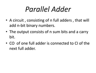
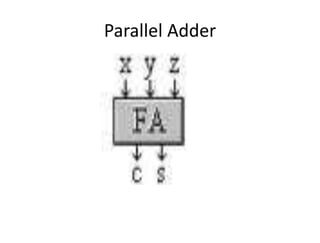
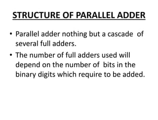
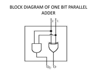
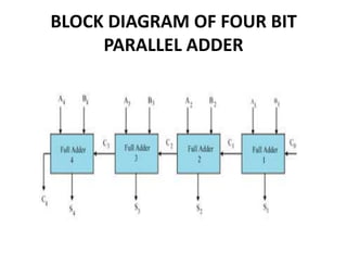
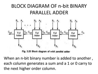
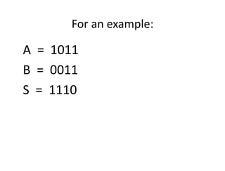
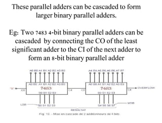
 A binary parallel adder is a
digital circuit that produces the
arithmetic sum of two binary
numbers in parallel.
STRUCTURE OF PARALLEL ADDER
• Parallel adder nothing but a cascade of
several full adders.
• The number of full adders used will
depend on the number of bits in the
binary digits which require to be added.
DIFFERENT TYPES OF BINNER ADDER
• ONE BIT PARALLEL ADDER
• TWO BIT PARALLER ADDER
• FOUR BIT PARALLER ADDER
BLOCK DIAGRAM OF ONE BIT PARALLEL
ADDER
BLOCK DIAGRAM OF TWO-BIT PARALLEL
ADDER
BLOCK DIAGRAM OF FOUR BIT
PARALLEL ADDER
BLOCK DIAGRAM OF n-bit BINARY
PARALLEL ADDER
When an n-bit binary number is added to another ,
each column generates a sum and a 1 or 0 carry to
the next higher order column.
For an example:
A = 1011
B = 0011
S = 1110
Demonstration:
subscript 4 3 2 1
Input carry 0 1 1 0 Ci
Augend 1 0 1 1 Ai
Addend 0 0 1 1 Bi
Sum 1 1 1 0 Si
Output carry 0 0 1 1 Ci+1
Procedure
The bits are added with full-adder.
Starting from the least significant position to
form the sum and carry.
The input carry CI1 in the least significant
position must be zero.
The value of CIi+1 in a given significant position is
the output carry CO of the full adder.
This value is transferred into the input carryCI of
the full-adder that adds the bits one higher
significant position to left.
The sum bits are thus generated starting from
the rightmost position and are available as soon
as the corresponding previous carry bit is
generated.
RIPPLE CARRY ADDER
A binary parallel adder
constructed this way is also called
ripple carry adder as the carry
output of each full-adder is
connected to the carry input of the
next higher-order stage.
Carry propagation delay
• The sum and the output carry of any
stage cannot be produced until the input
carry occurs ,this causes a time delay,
called the carry propagation delay
• The carry propagation delay for each full-
adder is the time from the application of
the input carry until the output carry occurs,
assuming that the A and B inputs are already
present.
Worst case
• The cumulative delay through all the
adder stages is a “worst case” addition
time.
• The total delay can vary, depending on
the carry bit produced by each full-adder.
IC
•Several configuration
of binary parallel
adders are available
in IC form.
•Popular
example:74283(4-bit
binary parallel adder)
These parallel adders can be cascaded to form
larger binary parallel adders.
Eg: Two 7483 4-bit binary parallel adders can be
cascaded by connecting the CO of the least
significant adder to the CI of the next adder to
form an 8-bit binary parallel adder
Binary parallel adder

Binary parallel adder

  • 2.
  • 3.
    Parallel Adder • Acircuit , consisting of n full adders , that will add n-bit binary numbers. • The output consists of n sum bits and a carry bit. • CO of one full adder is connected to CI of the next full adder.
  • 4.
  • 5.
    Serial Adder • Theserial adder is a binary adder that is capable of forming sum and carry outputs for addend and augend words of greater than one bit in length.
  • 7.
    Parallel & Serial Parallel •Faster. • It uses registers with parallel load capacity. • Number of full adder circuit is equal to number of bits in binary adder. • It is a combinational circuit. • Time required does not depend on the number of bits Serial • Slower • It uses shift registers. • It requires one full adder circuit. • It is sequential circuit. • Time required for addition depends on number of bits.
  • 9.
     A binaryparallel adder is a digital circuit that produces the arithmetic sum of two binary numbers in parallel.
  • 10.
    STRUCTURE OF PARALLELADDER • Parallel adder nothing but a cascade of several full adders. • The number of full adders used will depend on the number of bits in the binary digits which require to be added.
  • 11.
    DIFFERENT TYPES OFBINNER ADDER • ONE BIT PARALLEL ADDER • TWO BIT PARALLER ADDER • FOUR BIT PARALLER ADDER
  • 12.
    BLOCK DIAGRAM OFONE BIT PARALLEL ADDER
  • 13.
    BLOCK DIAGRAM OFTWO-BIT PARALLEL ADDER
  • 14.
    BLOCK DIAGRAM OFFOUR BIT PARALLEL ADDER
  • 15.
    BLOCK DIAGRAM OFn-bit BINARY PARALLEL ADDER When an n-bit binary number is added to another , each column generates a sum and a 1 or 0 carry to the next higher order column.
  • 16.
    For an example: A= 1011 B = 0011 S = 1110
  • 17.
    Demonstration: subscript 4 32 1 Input carry 0 1 1 0 Ci Augend 1 0 1 1 Ai Addend 0 0 1 1 Bi Sum 1 1 1 0 Si Output carry 0 0 1 1 Ci+1
  • 18.
    Procedure The bits areadded with full-adder. Starting from the least significant position to form the sum and carry. The input carry CI1 in the least significant position must be zero. The value of CIi+1 in a given significant position is the output carry CO of the full adder. This value is transferred into the input carryCI of the full-adder that adds the bits one higher significant position to left. The sum bits are thus generated starting from the rightmost position and are available as soon as the corresponding previous carry bit is generated.
  • 19.
    RIPPLE CARRY ADDER Abinary parallel adder constructed this way is also called ripple carry adder as the carry output of each full-adder is connected to the carry input of the next higher-order stage.
  • 20.
    Carry propagation delay •The sum and the output carry of any stage cannot be produced until the input carry occurs ,this causes a time delay, called the carry propagation delay • The carry propagation delay for each full- adder is the time from the application of the input carry until the output carry occurs, assuming that the A and B inputs are already present.
  • 21.
    Worst case • Thecumulative delay through all the adder stages is a “worst case” addition time. • The total delay can vary, depending on the carry bit produced by each full-adder.
  • 22.
    IC •Several configuration of binaryparallel adders are available in IC form. •Popular example:74283(4-bit binary parallel adder)
  • 23.
    These parallel adderscan be cascaded to form larger binary parallel adders. Eg: Two 7483 4-bit binary parallel adders can be cascaded by connecting the CO of the least significant adder to the CI of the next adder to form an 8-bit binary parallel adder