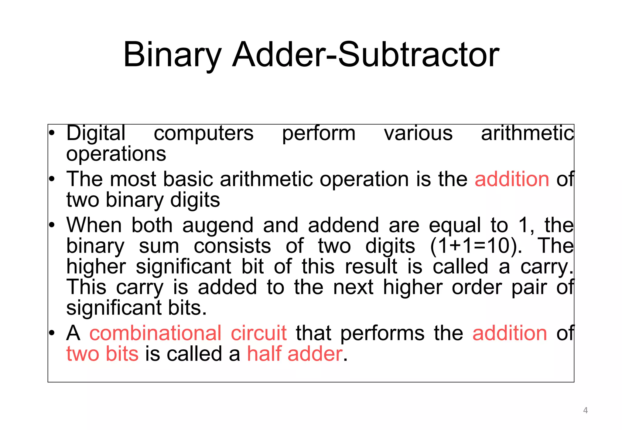
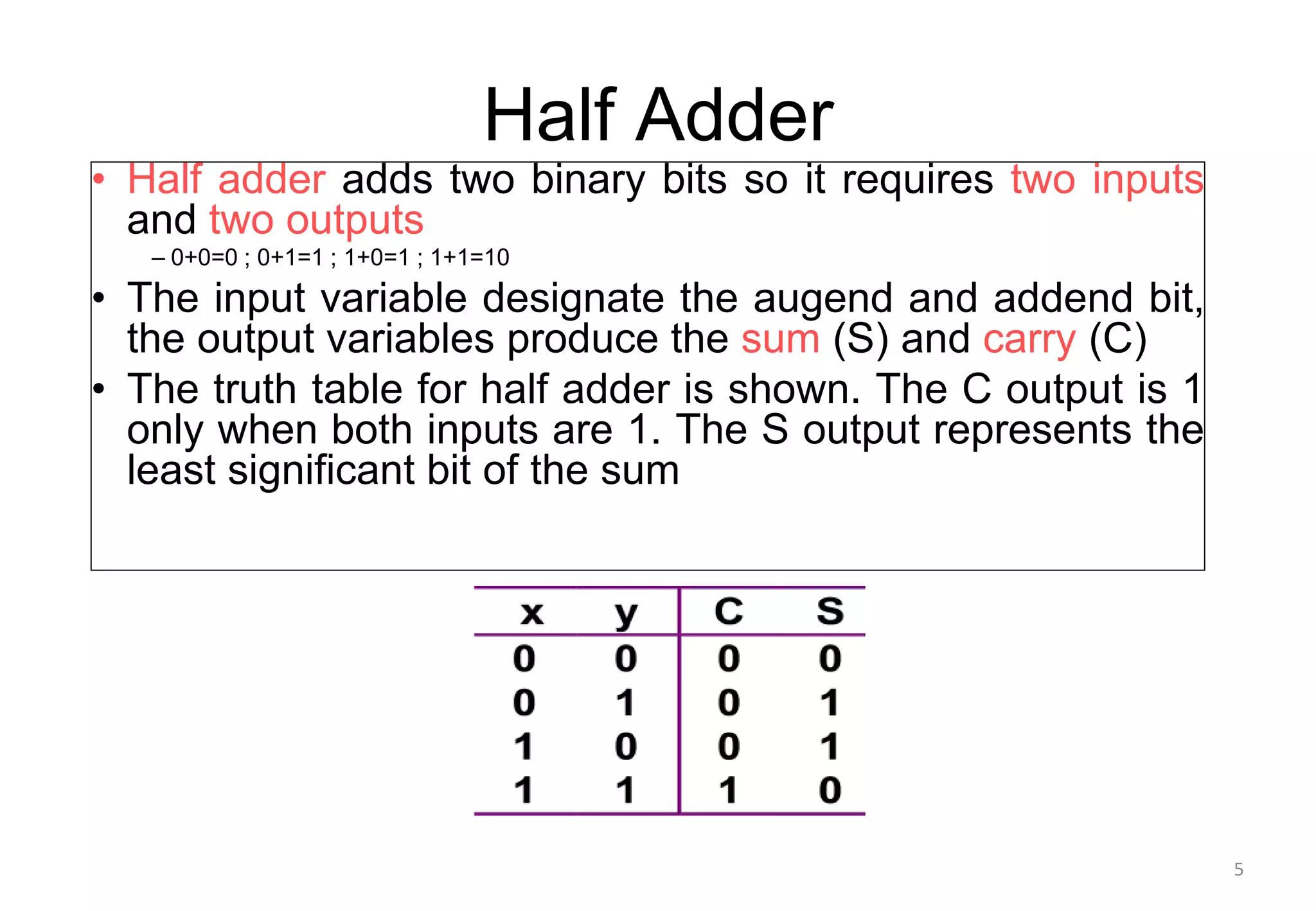
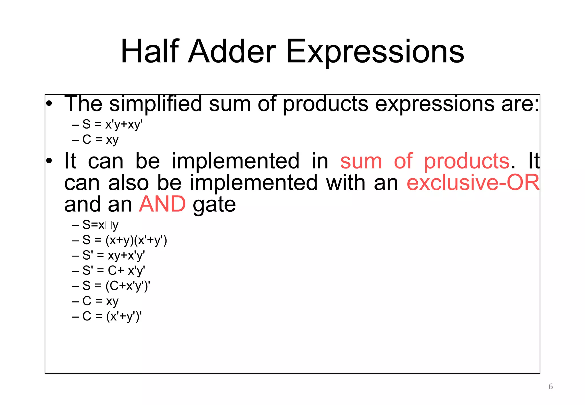
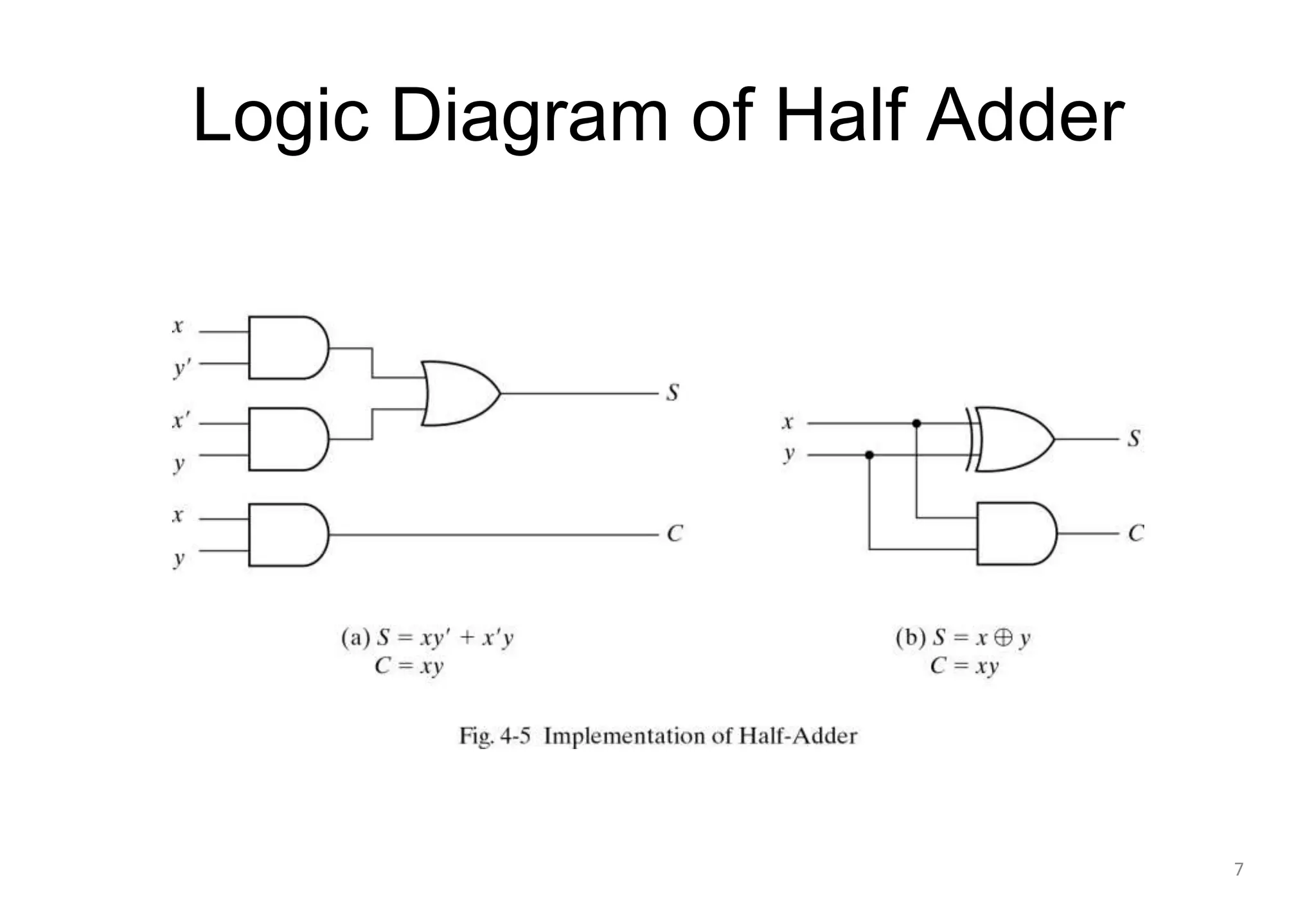
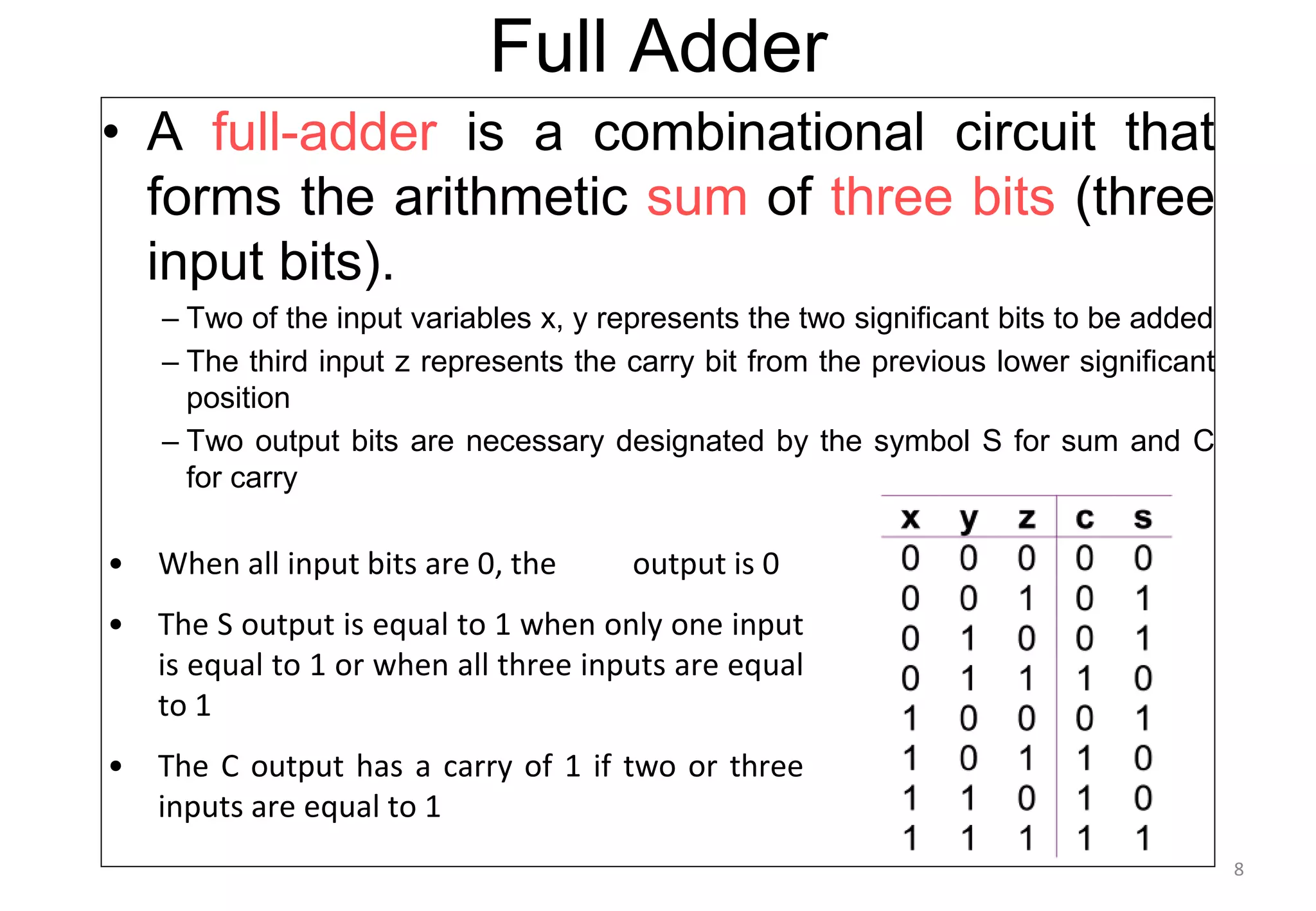
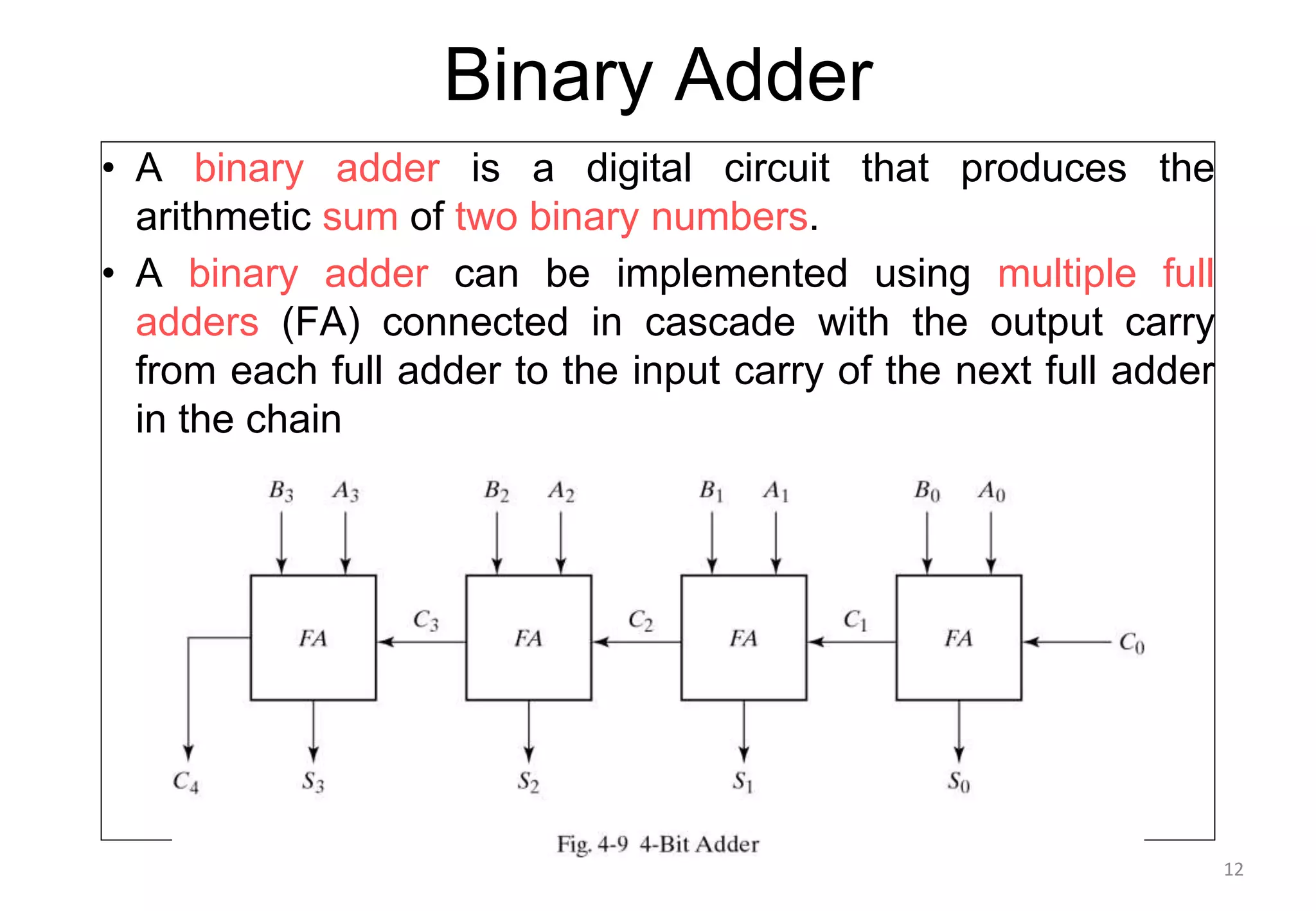
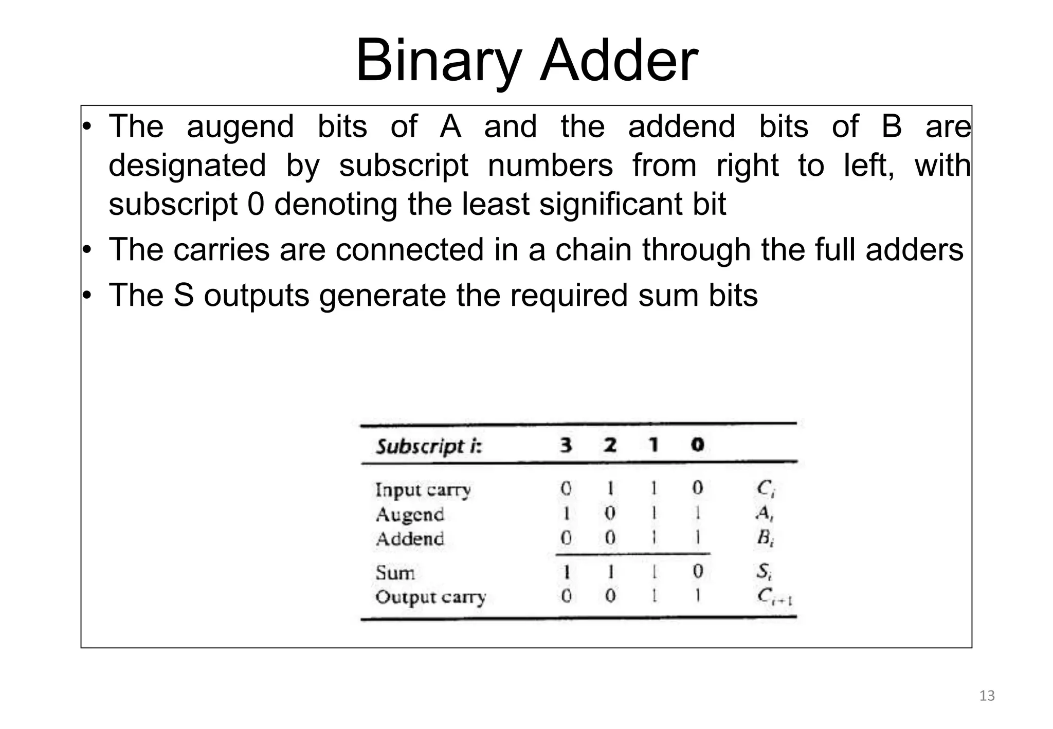
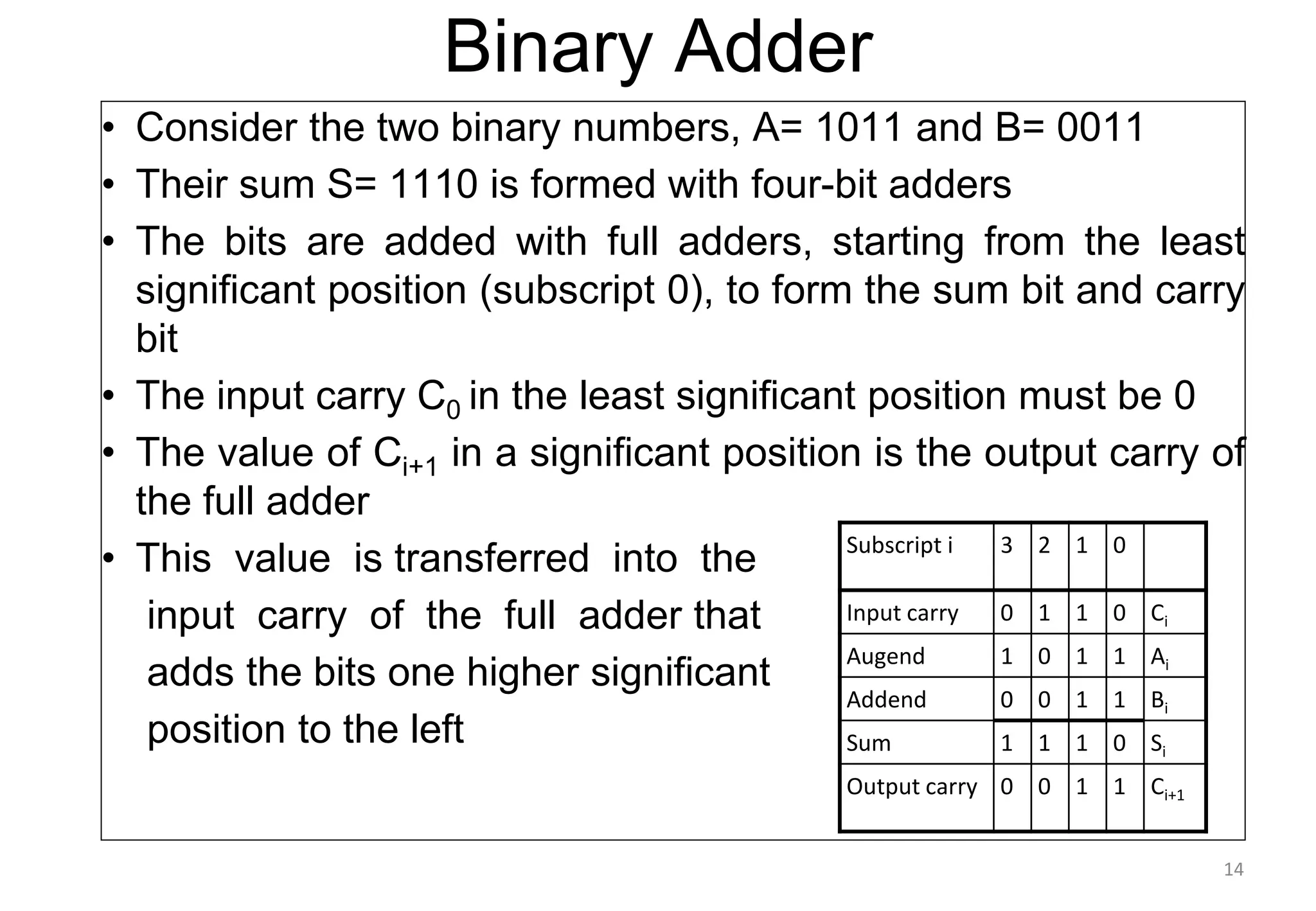
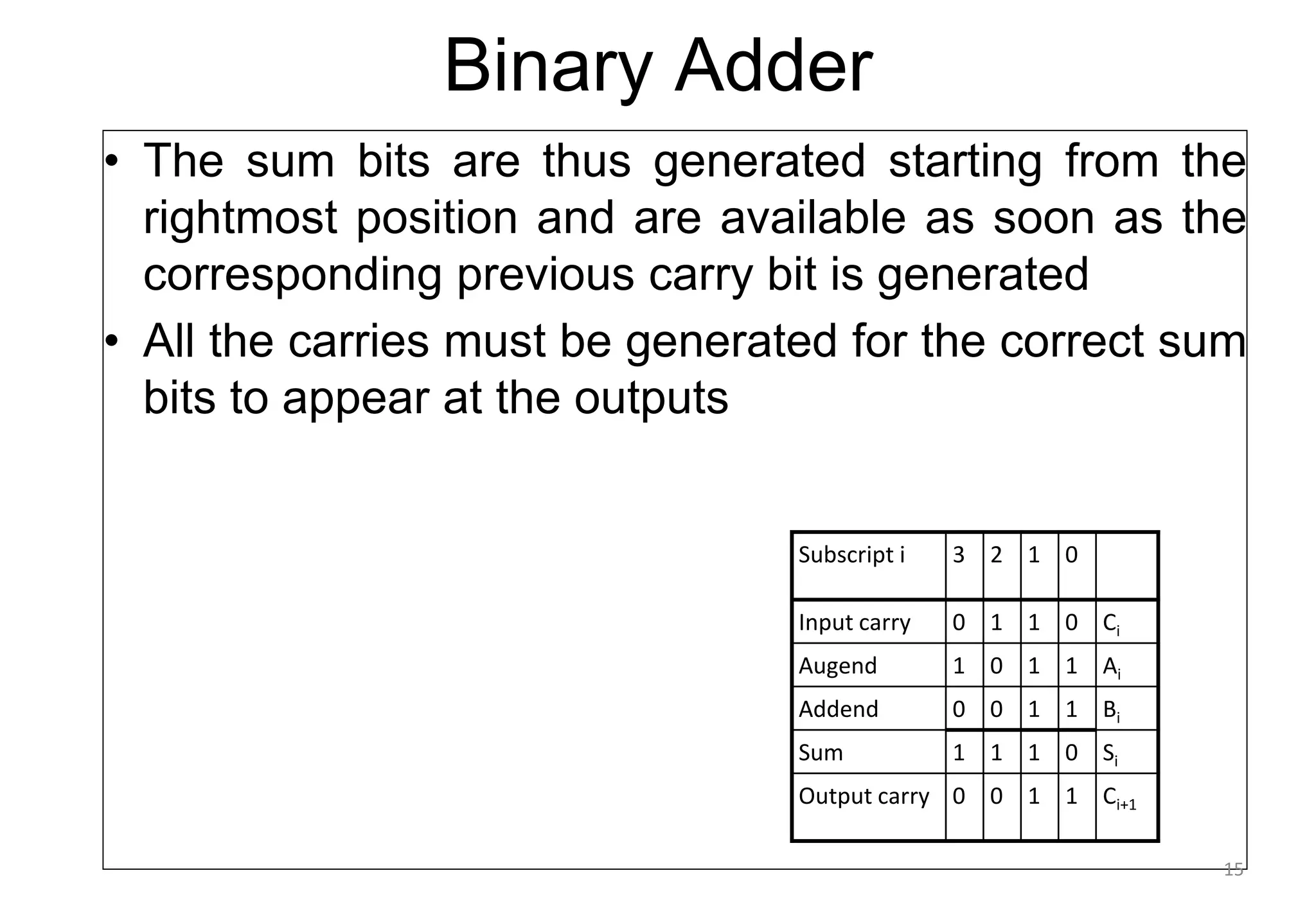
Digital Logic and Design
Lecture No 19 : Binary Adders, Subtractors
1
Overview of Last Lecture
• Analysis of Combinational Circuit
• Combinational Design
• BCD to Excess-3 Code Converter
• BCD to Seven Segment Display code
converter
• Binary to Dice Display code converter
2
Today’s Lecture
• Binary Adder-Subtractor
– Half Adder
– Full Adder
• Carry Lookahead Generator
3
Binary Adder-Subtractor
• Digital computers perform various arithmetic
operations
• The most basic arithmetic operation is the addition of
two binary digits
• When both augend and addend are equal to 1, the
binary sum consists of two digits (1+1=10). The
higher significant bit of this result is called a carry.
This carry is added to the next higher order pair of
significant bits.
• A combinational circuit that performs the addition of
two bits is called a half adder.
4
Half Adder
• Half adder adds two binary bits so it requires two inputs
and two outputs
– 0+0=0 ; 0+1=1 ; 1+0=1 ; 1+1=10
• The input variable designate the augend and addend bit,
the output variables produce the sum (S) and carry (C)
• The truth table for half adder is shown. The C output is 1
only when both inputs are 1. The S output represents the
least significant bit of the sum
5
Half Adder Expressions
• The simplified sum of products expressions are:
– S = x'y+xy'
– C = xy
• It can be implemented in sum of products. It
can also be implemented with an exclusive-OR
and an AND gate
– S=xy
– S = (x+y)(x'+y')
– S' = xy+x'y'
– S' = C+ x'y'
– S = (C+x'y')'
– C = xy
– C = (x'+y')'
6
Logic Diagram of Half Adder
7
Full Adder
• A full-adder is a combinational circuit that
forms the arithmetic sum of three bits (three
input bits).
– Two of the input variables x, y represents the two significant bits to be added
– The third input z represents the carry bit from the previous lower significant
position
– Two output bits are necessary designated by the symbol S for sum and C
for carry
• When all input bits are 0, the output is 0
• The S output is equal to 1 when only one input
is equal to 1 or when all three inputs are equal
to 1
• The C output has a carry of 1 if two or three
inputs are equal to 1
8
Maps for Full Adder
9
Simplified Expressions for Full Adder
• The simplified expressions for full adder are
– S = x' y' z + x' y z' + x y' z' + x y z
– C = xy + xz + yz
10
Full Adder with Two Half Adders
• Full adder can also be implemented with two half
adders and an OR gate. The S output from the
second half adder is the exclusive-OR of z and
the output of the first half adder giving
– S = z  (x  y)
= z'(xy'+x'y)+z(xy'+x'y)'
=z'(xy'+x'y)+z(xy+x'y')
= xy'z'+x'yz'+xyz+x'y'z
– C = z(xy'+x'y)+xy
= xy'z+x'yz+ xy
Half adder
11
Binary Adder
• A binary adder is a digital circuit that produces the
arithmetic sum of two binary numbers.
• A binary adder can be implemented using multiple full
adders (FA) connected in cascade with the output carry
from each full adder to the input carry of the next full adder
in the chain
12
Binary Adder
• The augend bits of A and the addend bits of B are
designated by subscript numbers from right to left, with
subscript 0 denoting the least significant bit
• The carries are connected in a chain through the full adders
• The S outputs generate the required sum bits
13
Binary Adder
• Consider the two binary numbers, A= 1011 and B= 0011
• Their sum S= 1110 is formed with four-bit adders
• The bits are added with full adders, starting from the least
significant position (subscript 0), to form the sum bit and carry
bit
• The input carry C0 in the least significant position must be 0
• The value of Ci+1 in a significant position is the output carry of
the full adder
• This value is transferred into the
input carry of the full adder that
adds the bits one higher significant
position to the left
Subscript i 3 2 1 0
Input carry 0 1 1 0 Ci
Augend 1 0 1 1 Ai
Addend 0 0 1 1 Bi
Sum 1 1 1 0 Si
Output carry 0 0 1 1 Ci+1
14
Binary Adder
• The sum bits are thus generated starting from the
rightmost position and are available as soon as the
corresponding previous carry bit is generated
• All the carries must be generated for the correct sum
bits to appear at the outputs
Subscript i 3 2 1 0
Input carry 0 1 1 0 Ci
Augend 1 0 1 1 Ai
Addend 0 0 1 1 Bi
Sum 1 1 1 0 Si
Output carry 0 0 1 1 Ci+1
15
Carry Propagation
• The addition of two binary numbers in parallel implies
that all the bits of the augend and addend are
available for computation at the same time
• In any combinational circuit, the signal must
propagate through the gates before the correct
output is available in the output terminals.
• The Total propagation time = the propagation delay
of a typical gate X the number of gate levels
• The longest propagation delay time in a binary adder
is the time it takes the carry to propagate through the
full adders.
• This is because each bit of the sum output depends
on the value of the input carry. This makes the binary
adder very slow.
16
Carry Propagation
• Since each bit of the sum output depends on the value of
input carry, the value of Si in any given stage in the adder
will be in its steady state final value only after the input
carry to the stage has been propagated
• Consider output S3 in figure 4-9. Inputs A3 and B3 are
available as soon as input signals are applied to the
adder, however input carry C3 doesn’t settle to its final
value until C2 is available from the previous stage
• Similarly C2 has to wait for C1 and so on down to C0
• In this way only after the carry propagates and ripples
through all stages will the last output S3 and carry C4
settle to their final correct value
17
Carry Propagation
• The number of gate levels for the carry propagation can be
found from the circuit of the full adder
• The input and output variables use the subscript i to denote
a typical stage in the adder
• The signals at Pi and Gi settle to their steady state values
after they propagate through their respective gates
18
End of Lecture
19

DLD Lecture No 19 Binary adders.pptx

  • 1.
    Digital Logic andDesign Lecture No 19 : Binary Adders, Subtractors 1
  • 2.
    Overview of LastLecture • Analysis of Combinational Circuit • Combinational Design • BCD to Excess-3 Code Converter • BCD to Seven Segment Display code converter • Binary to Dice Display code converter 2
  • 3.
    Today’s Lecture • BinaryAdder-Subtractor – Half Adder – Full Adder • Carry Lookahead Generator 3
  • 4.
    Binary Adder-Subtractor • Digitalcomputers perform various arithmetic operations • The most basic arithmetic operation is the addition of two binary digits • When both augend and addend are equal to 1, the binary sum consists of two digits (1+1=10). The higher significant bit of this result is called a carry. This carry is added to the next higher order pair of significant bits. • A combinational circuit that performs the addition of two bits is called a half adder. 4
  • 5.
    Half Adder • Halfadder adds two binary bits so it requires two inputs and two outputs – 0+0=0 ; 0+1=1 ; 1+0=1 ; 1+1=10 • The input variable designate the augend and addend bit, the output variables produce the sum (S) and carry (C) • The truth table for half adder is shown. The C output is 1 only when both inputs are 1. The S output represents the least significant bit of the sum 5
  • 6.
    Half Adder Expressions •The simplified sum of products expressions are: – S = x'y+xy' – C = xy • It can be implemented in sum of products. It can also be implemented with an exclusive-OR and an AND gate – S=xy – S = (x+y)(x'+y') – S' = xy+x'y' – S' = C+ x'y' – S = (C+x'y')' – C = xy – C = (x'+y')' 6
  • 7.
    Logic Diagram ofHalf Adder 7
  • 8.
    Full Adder • Afull-adder is a combinational circuit that forms the arithmetic sum of three bits (three input bits). – Two of the input variables x, y represents the two significant bits to be added – The third input z represents the carry bit from the previous lower significant position – Two output bits are necessary designated by the symbol S for sum and C for carry • When all input bits are 0, the output is 0 • The S output is equal to 1 when only one input is equal to 1 or when all three inputs are equal to 1 • The C output has a carry of 1 if two or three inputs are equal to 1 8
  • 9.
  • 10.
    Simplified Expressions forFull Adder • The simplified expressions for full adder are – S = x' y' z + x' y z' + x y' z' + x y z – C = xy + xz + yz 10
  • 11.
    Full Adder withTwo Half Adders • Full adder can also be implemented with two half adders and an OR gate. The S output from the second half adder is the exclusive-OR of z and the output of the first half adder giving – S = z  (x  y) = z'(xy'+x'y)+z(xy'+x'y)' =z'(xy'+x'y)+z(xy+x'y') = xy'z'+x'yz'+xyz+x'y'z – C = z(xy'+x'y)+xy = xy'z+x'yz+ xy Half adder 11
  • 12.
    Binary Adder • Abinary adder is a digital circuit that produces the arithmetic sum of two binary numbers. • A binary adder can be implemented using multiple full adders (FA) connected in cascade with the output carry from each full adder to the input carry of the next full adder in the chain 12
  • 13.
    Binary Adder • Theaugend bits of A and the addend bits of B are designated by subscript numbers from right to left, with subscript 0 denoting the least significant bit • The carries are connected in a chain through the full adders • The S outputs generate the required sum bits 13
  • 14.
    Binary Adder • Considerthe two binary numbers, A= 1011 and B= 0011 • Their sum S= 1110 is formed with four-bit adders • The bits are added with full adders, starting from the least significant position (subscript 0), to form the sum bit and carry bit • The input carry C0 in the least significant position must be 0 • The value of Ci+1 in a significant position is the output carry of the full adder • This value is transferred into the input carry of the full adder that adds the bits one higher significant position to the left Subscript i 3 2 1 0 Input carry 0 1 1 0 Ci Augend 1 0 1 1 Ai Addend 0 0 1 1 Bi Sum 1 1 1 0 Si Output carry 0 0 1 1 Ci+1 14
  • 15.
    Binary Adder • Thesum bits are thus generated starting from the rightmost position and are available as soon as the corresponding previous carry bit is generated • All the carries must be generated for the correct sum bits to appear at the outputs Subscript i 3 2 1 0 Input carry 0 1 1 0 Ci Augend 1 0 1 1 Ai Addend 0 0 1 1 Bi Sum 1 1 1 0 Si Output carry 0 0 1 1 Ci+1 15
  • 16.
    Carry Propagation • Theaddition of two binary numbers in parallel implies that all the bits of the augend and addend are available for computation at the same time • In any combinational circuit, the signal must propagate through the gates before the correct output is available in the output terminals. • The Total propagation time = the propagation delay of a typical gate X the number of gate levels • The longest propagation delay time in a binary adder is the time it takes the carry to propagate through the full adders. • This is because each bit of the sum output depends on the value of the input carry. This makes the binary adder very slow. 16
  • 17.
    Carry Propagation • Sinceeach bit of the sum output depends on the value of input carry, the value of Si in any given stage in the adder will be in its steady state final value only after the input carry to the stage has been propagated • Consider output S3 in figure 4-9. Inputs A3 and B3 are available as soon as input signals are applied to the adder, however input carry C3 doesn’t settle to its final value until C2 is available from the previous stage • Similarly C2 has to wait for C1 and so on down to C0 • In this way only after the carry propagates and ripples through all stages will the last output S3 and carry C4 settle to their final correct value 17
  • 18.
    Carry Propagation • Thenumber of gate levels for the carry propagation can be found from the circuit of the full adder • The input and output variables use the subscript i to denote a typical stage in the adder • The signals at Pi and Gi settle to their steady state values after they propagate through their respective gates 18
  • 19.