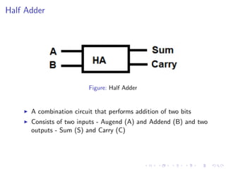
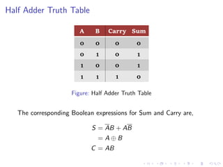
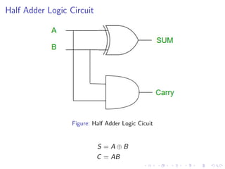
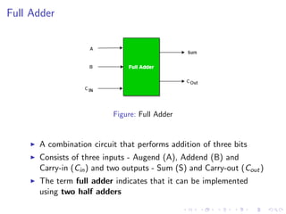
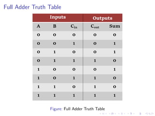
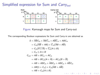
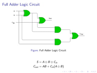
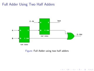
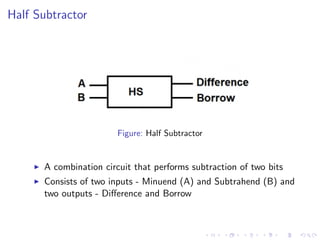
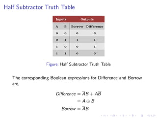
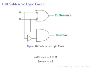
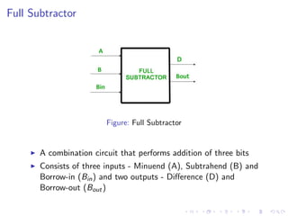
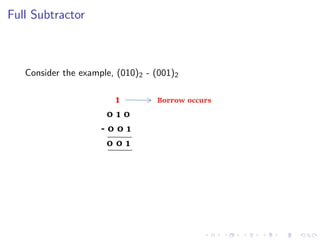
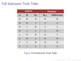
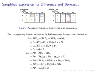
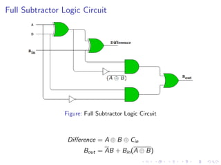
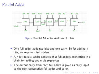
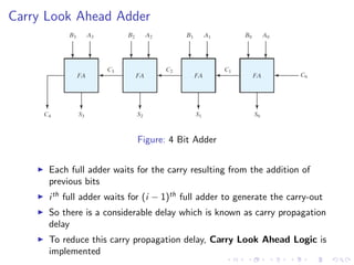
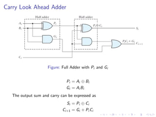
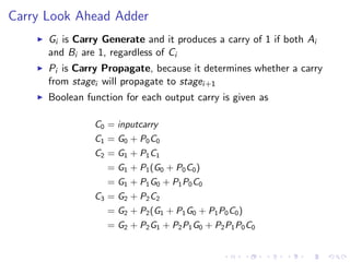
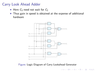
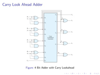
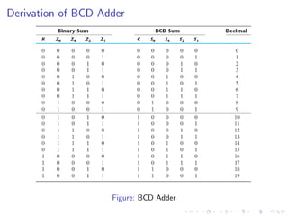
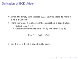
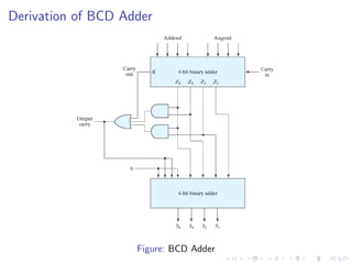
The document describes various binary adders and subtractors used in digital circuits, including half adders, full adders, half subtractors, full subtractors, parallel adders, carry lookahead adders, and BCD adders. It explains their logic functions, truth tables, logic circuits, and implementations. It also provides examples of problems involving calculating propagation delays of ripple carry adders with different bit sizes and gate delays.


![Problem 1
[GATE-CS-2015] A half adder is implemented with XOR and AND
gates. A full adder is implemented with two half adders and one
OR gate. The propagation delay of an XOR gate is twice that of
an AND/OR gate. The propagation delay of an AND/OR gate is
1.2 microseconds. A 4-bit ripple-carry binary adder is implemented
by using full adders. The total propagation time of this 4-bit
binary adder in microseconds is](https://image.slidesharecdn.com/binaryadders-230720150814-2ac346d0/85/Binary-Adders-pdf-28-320.jpg)
![Problem 1
[GATE-CS-2015] A half adder is implemented with XOR and AND
gates. A full adder is implemented with two half adders and one
OR gate. The propagation delay of an XOR gate is twice that of
an AND/OR gate. The propagation delay of an AND/OR gate is
1.2 microseconds. A 4-bit ripple-carry binary adder is implemented
by using full adders. The total propagation time of this 4-bit
binary adder in microseconds is](https://image.slidesharecdn.com/binaryadders-230720150814-2ac346d0/85/Binary-Adders-pdf-29-320.jpg)
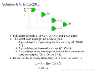
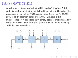
![Solution GATE-CS-2015
A half adder is implemented with XOR and AND gates. A full
adder is implemented with two half adders and one OR gate. The
propagation delay of an XOR gate is twice that of an AND/OR
gate. The propagation delay of an AND/OR gate is 1.2
microseconds. A 4-bit ripple-carry binary adder is implemented by
using full adders. The total propagation time of this 4-bit binary
adder in microseconds is
Answer: 4[(2n+2)*1.2] = 19.2ms](https://image.slidesharecdn.com/binaryadders-230720150814-2ac346d0/85/Binary-Adders-pdf-32-320.jpg)
![Problem 2
[GATE-EC-2017] Figure I shows a 4-bit ripple carry adder realized using
full adders and Figure II shows the circuit of a full-adder (FA). The
propagation delay of the XOR, AND and OR gates in Figure II are 20 ns,
15 ns and 10 ns, respectively. Assume all the inputs to the 4-bit adder
are initially reset to 0.
At t = 0, the input to the 4-bit adder are changed to A3A2A1A0 = 1100,
B3B2B1B0 = 0100 and C0 = 1. The output of the ripple carry adder will
be stable at t (in ns)=](https://image.slidesharecdn.com/binaryadders-230720150814-2ac346d0/85/Binary-Adders-pdf-33-320.jpg)
![Problem 2
[GATE-EC-2017] Figure I shows a 4-bit ripple carry adder realized using
full adders and Figure II shows the circuit of a full-adder (FA). The
propagation delay of the XOR, AND and OR gates in Figure II are 20 ns,
15 ns and 10 ns, respectively. Assume all the inputs to the 4-bit adder
are initially reset to 0.
At t = 0, the input to the 4-bit adder are changed to A3A2A1A0 = 1100,
B3B2B1B0 = 0100 and C0 = 1. The output of the ripple carry adder will
be stable at t (in ns)=
Solution: Link](https://image.slidesharecdn.com/binaryadders-230720150814-2ac346d0/85/Binary-Adders-pdf-34-320.jpg)
![Problem 3
[GATE ECE 2014 Set 4] A 16-bit ripple carry adder is realized
using 16 identical full adders (FA) as shown in the figure. The
carry-propagation delay of each FA is 12 ns and the sum
propagation delay of each FA is 15 ns. The worst case delay (in ns)
of this 16-bit adder will be](https://image.slidesharecdn.com/binaryadders-230720150814-2ac346d0/85/Binary-Adders-pdf-35-320.jpg)
![Problem 3
[GATE ECE 2014 Set 4] A 16-bit ripple carry adder is realized
using 16 identical full adders (FA) as shown in the figure. The
carry-propagation delay of each FA is 12 ns and the sum
propagation delay of each FA is 15 ns. The worst case delay (in ns)
of this 16-bit adder will be
Answer: For the 1st FA, the carry propagation delay is 12 ns. So
the 2nd FA will generate its carry after 24ns. Therefore, the worst
case delay is = (15*12) + 15 = 195 ns](https://image.slidesharecdn.com/binaryadders-230720150814-2ac346d0/85/Binary-Adders-pdf-36-320.jpg)


![[Deck] What's New in Spark-Iceberg Integration via DSV2.pptx](https://cdn.slidesharecdn.com/ss_thumbnails/deckwhatsnewinspark-icebergintegrationviadsv2-260210005337-25955b12-thumbnail.jpg?width=640&height=640&fit=bounds)


