Download to read offline

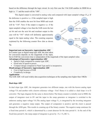
![When the counter reaches
the fixed count at time
period t1, the binary
counter resets to 0000 and
switches the integrator
input to a negative
reference voltage –Vref.
Now the ramp generator
starts with the initial value –Vs and increases in positive direction until it reaches 0V and the counter gets
advanced. When Vs reaches 0V, comparator output becomes negative (i.e. logic 0) and the AND gate is
deactivated. Hence no further clock is
applied through AND gate. Now, the
conversion cycle is said to be completed and
the positive ramp voltage is given by
∴VS=Vref/RC×t2
Where Vref & RC are constants and time
period t2 is variable. The dual ramp output
waveform is shown below. Since ramp generator voltage starts at 0V, decreasing down to –Vs and then
increasing up to 0V, the amplitude of negative and positive ramp voltages can be equated as follows.
∴Vref/RC×t2=-VA/RC×t1
∴t2=-t1×VA/Vref
∴VA=-Vref×t1/t2
Thus the unknown analog input voltage VA is proportional to the time period t2, because Vref is a known
reference voltage and t1 is the predetermined time period. The actual conversion of analog voltage VA into
a digital count occurs during time t2. The binary counter gives corresponding digital value for time period
t2. The clock is connected to the counter at the beginning of t2 and is disconnected at the end of t2.
Thus the counter counts digital output as Digital output=(counts/sec) t2
∴Digital output=(counts/sec)[t1×VA/Vref ]](https://image.slidesharecdn.com/unit3-200828101111/85/Analog-IC-Application-9-320.jpg)

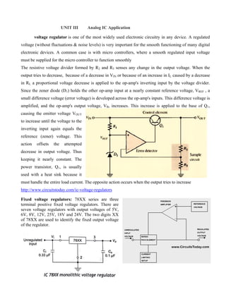
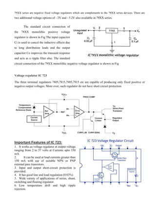
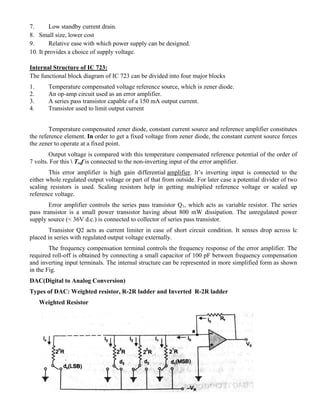
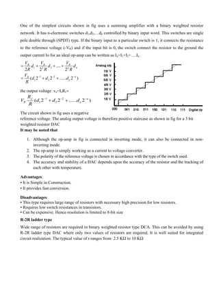
The document discusses voltage regulators and digital to analog converters (DACs). It provides details on: 1) How voltage regulators work to keep an output voltage constant by sensing changes and amplifying any difference between the output and a reference voltage. 2) Common types of voltage regulators including fixed voltage 78XX series and adjustable voltage 723 series. 3) Types of DACs including weighted resistor, R-2R ladder, and inverted R-2R ladder; and how their resistor networks convert a digital input to an analog output voltage. 4) How successive approximation and dual slope ADCs work to convert an analog input to digital output using comparison and feedback to approximate or time the input voltage.