Chapter 5     Differential and Multistage Amplifier
Outline Introduction The CMOS Differential Pair Small-Signal Operation of the MOS Differential Pair The BJT Differential Pair The differential Amplifier with Active Load Frequency Response of the Differential  amplifier Multistage Amplifiers
Introduction Two reasons of the differential amplifier suited for IC fabrication: IC fabrication is capable of providing matched devices. Utilizing more components than single-ended amplifier: Differential circuits are much less sensitive to noise and interference. Differential configuration enable us to bias the amplifier and to couple amplifier stages without the need for bypass and coupling capacitors.
The MOS Differential Pair Basic structure of differential pair. Characteristics
The MOS Differential Pair
Operation with a Common –Mode Input Voltage
Operation with a Common –Mode Input Voltage Symmetry circuit. Common-mode voltage. Current  I  divides equally between two transistors. The difference between two drains is zero. The differential pair rejects the common-mode input signals.
Operation with a Differential  Input Voltage The MOS differential pair with a differential input signal  v id  applied.  With  v id  positive:  v GS 1      v GS 2 ,  i D 1      i D 2 , and  v D 1      v D 2 ; thus ( v D 2      v D 1 ) will be positive.  With  v id  negative:  v GS 1      v GS 2 ,  i D 1      i D 2 , and  v D 1      v D 2 ; thus ( v D 2      v D 1 ) will be negative.
Operation with a Differential  Input Voltage Differential input voltage. Response to the differential input signal. The current  I  can be steered from one transistor to the other by varying the differential input voltage in the range: When differential input voltage is very small, the differential output voltage is proportional to it, and the gain is high.
Large-Signal Operation Transfer characteristic curves Normalized plots of the currents in a MOSFET differential pair.  Note that  V OV  is the overdrive voltage at which  Q 1  and  Q 2  operate when conducting drain currents equal to  I /2.
Large-Signal Operation Nonlinear curves. Maximum value of input differential voltage. When  v id   = 0, two drain currents are equal to  I/2. Linear segment. Linearity can be increased by increasing overdrive voltage(see next slide). Price paid is a reduction in gain(current  I  is kept constant).
Large-Signal Operation The linear range of operation of the MOS differential pair can be extended by operating the transistor at a higher value of  V OV .
Small-Signal Operation of MOS Differential Pair Linear amplifier Differential gain Common-mode gain Common-mode rejection ratio(CMRR) Mismatch on CMRR
Differential Gain a common-mode voltage applied to set the dc bias voltage at the gates. v id  applied in a complementary (or balanced) manner.
Differential Gain Signal voltage at the joint source connection must be zero.
Differential Gain An alternative way of looking at the small-signal operation of the circuit .
Differential Gain Differential gain Output taken single-ended Output taken differentially Advantages of output signal taken differentially Reject common-mode signal Increase in gain by a factor of 2(6dB)
Differential Gain MOS differential amplifier with  r o  and  R SS  taken into account.
Differential Gain Equivalent circuit for determining the differential gain.  Each of the two halves of the differential amplifier circuit is a common-source amplifier, known as its differential “half-circuit.”
Differential Gain Differential gain Output taken single-ended Output taken differentially
Common-Mode Gain The MOS differential amplifier with a common-mode input signal  v icm .
Common-Mode Gain Equivalent circuit for determining the common-mode gain (with  r o  ignored). Each half of the circuit is known as the “common-mode half-circuit.”
Common-Mode Gain Common-mode gain Output taken single-ended Output taken differentially
Common-Mode Rejection Ratio Common-mode rejection ratio(CMRR) Output taken single-ended Output taken differentially This is true only when the circuit is perfectly matched.
Mismatch on CMRR Effect of  R D  mismatch on CMRR Effect of  g m  mismatch on CMRR
Mismatch on CMRR Determine the common-mode gain resulting from a mismatch in the  g m  values of  Q 1  and  Q 2 . Common-mode half circuit is not available due to mismatch in circuit. The nominal value  g m .
Mismatch on CMRR Effect of  g m  mismatch on CMRR
The BJT Differential Pair Basic operation Large-signal operation Small-signal operation Differential gain Common-mode gain Common-mode rejection ration
The BJT Differential Pair The basic BJT differential-pair configuration.
Basic Operation The differential pair with a common-mode input signal  v CM .  Two transistors are matched. Current source with infinite output resistance. Current I divide equally between two transistors. The difference in voltage between the two collector is zero. The differential pair rejects the common-mode input signal as long as two transistors remain in active region.
Basic Operation The differential pair with a “large” differential input signal. Q 1  is on and Q 2  is off. Current I entirely flows in Q 1 .
Basic Operation The differential pair with a large differential input signal of polarity opposite to that in (b).  Q 2  is on and Q 1  is off. Current I entirely flows in Q 2 .
Basic Operation The differential pair with a small differential input signal  v i . Small signal operation or linear amplifier.  Assuming the bias current source  I  to be ideal and thus  I  remains constant with the change in  v CM . Increment in Q 1  and decrement in Q 2 .
Large-Signal Operation
Large-Signal Operation Nonlinear curves. Linear segments. Maximum value of input differential voltages Enlarge the linear segment by including equal resistance  R e  in series with the emitters.
Large-Signal Operation The transfer characteristics of the BJT differential pair  (a)  can be linearized by including resistances in the emitters.
Small Signal Operation The currents and voltages in the differential amplifier when a small differential input signal  v id  is applied.
Small Signal Operation A simple technique for determining the signal currents in a differential amplifier excited by a differential voltage signal  v id ; dc quantities are not shown.
Small Signal Operation A differential amplifier with emitter resistances.  Only signal quantities are shown (in color).
Input Differential Resistance Input differential resistance is finite. The resistance seen between the two bases is equal to the total resistance in the emitter circuit multiplied by (1+ β).   Input differential resistance of differential pair with emitter resistors.
Differential Voltage Gain Differential voltage gain Output voltage taken single-ended Output voltage taken differentially
Differential Voltage Gain Differential voltage gain of the differential pair with resistances in the emitter leads Output voltage taken single-ended Output voltage taken differentially The voltage gain is equal to the ratio of the total resistance in the collector circuit to the total resistance in the emitter circuit.
Differential Half-Circuit Analysis Differential input signals. Single voltage at joint emitters is zero. The circuit is symmetric.  Equivalent common-emitter amplifiers in (b).
Differential Half-Circuit Analysis This equivalence applies only for differential input signals. Either of the two common-emitter amplifiers can be used to find the differential gain, differential input resistance, frequency response, and so on, of the differential amplifier. Half circuit is biased at  I/2. The voltage gain(with the output taken differentially) is equal to the voltage of half circuit.
Differential Half-Circuit Analysis The differential amplifier fed in a single-ended fashion. Signal voltage at the emitter is not zero. Almost identical to the symmetric one.
Common-Mode Gain  The differential amplifier fed by a common-mode voltage signal  v icm .
Common-Mode Gain  Equivalent “half-circuits” for common-mode calculations.
Common-Mode Gain  Common-mode voltage gain Output voltage taken single-ended Output voltage taken differentially
Common-Mode Rejection Ratio  Common-mode rejection ratio Output voltage taken single-ended Output voltage taken differentially This is true only when the circuit is symmetric. Mismatch on CMRR
Input Common-Mode Resistance  Definition of the input common-mode resistance  R icm .  The equivalent common-mode half-circuit.
Input Common-Mode Resistance  Input common-mode resistance Input common-mode resistance is very large.
Example
Example (cont’d)  Evaluate the following: The input differential resistance. The overall differential voltage gain(neglect the effect of  r o ). The worst-case common-mode gain if the two collector resistance are accurate within  ±1%. The CMRR, in dB. The input common-mode resistance(suppose the Early voltage is 100V).
The Differential Amplifier with Active Load Replace resistance  R D  with a constant current source results in a much high voltage gain as well as saving in chip area. Convert the output from differential to single-ended.
Differential-to-Single-Ended Conversion A simple but inefficient approach for differential to single-ended conversion.
The Active-Loaded MOS Differential Pair The active-loaded MOS differential pair.
The Active-Loaded MOS Differential Pair The circuit at equilibrium assuming perfect matching.
The Active-Loaded MOS Differential Pair The circuit with a differential input signal applied, neglecting the  r o  of all transistors.
Differential Gain of the Active-Loaded MOS Pair The output resistance  r o  plays a significant role in the operation of active-loaded amplifier. Asymmetric circuit. Half-circuit is not available. The gain will be determined as  G m R o
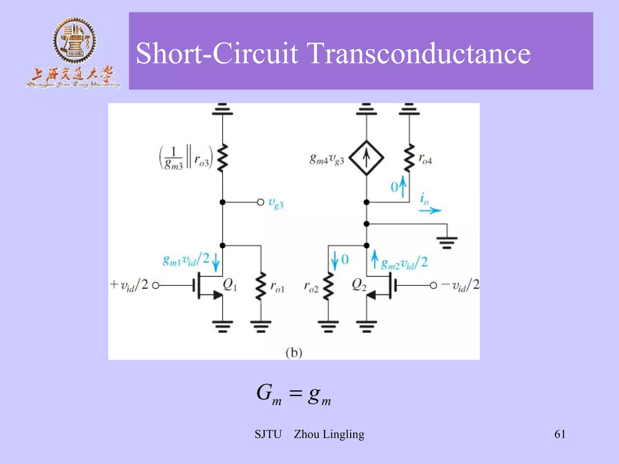
Short-Circuit Transconductance Determining the short-circuit transconductance  G m   =  i o / v id
Short-Circuit Transconductance
Output Resistance Circuit for determining  R o . The circled numbers indicate the order of the analysis steps.
Output Resistance Circuit for determining  R o .  The circled numbers indicate the order of the analysis steps.
Differential Gain The differential gain is determined as  G m R o When
Common-Mode Gain and CMRR Analysis of the active-loaded MOS differential amplifier to determine its common-mode gain. Power supplies eliminated. R ss  is the output resistance of the current source.
Common-Mode Gain and CMRR Asymmetric circuit. Each of the two transistors as a CS configuration with a large source degeneration resistance  2R ss. Common-mode gain: CMRR
The Bipolar Differential Pair with Active Load Active-loaded bipolar differential pair.
Determine the Transconductance
Determine the output Resistance
Differential Gain The differential gain is determined as  G m R o When  Input differential resistance
Common-Mode Gain and CMRR Common-mode gain: CMRR
Frequency Response of the Resistively Loaded MOS Amplifier A resistively loaded MOS differential pair with the transistor supplying the bias current explicitly shown.  It is assumed that the total impedance between node  S  and ground,  Z SS , consists of a resistance  R SS  in parallel with a capacitance  C SS .
Frequency Response of the Resistively Loaded MOS Amplifier (b)  Differential half-circuit.  (c)  Common-mode half-circuit.
Frequency Response of the Resistively Loaded MOS Amplifier common-mode gain
Frequency Response of the Resistively Loaded MOS Amplifier Differential Gain
Frequency Response of the Resistively Loaded MOS Amplifier CMRR with frequency.
Multistage Amplifier A four-stage bipolar op amplifier A two-stage CMOS op amplifier
Multistage Amplifier
Multistage Amplifier The first stage(input stage) is differential-in, differential-out and consists of Q 1  and Q 2 . The second stage is differential-in, single-ended-out amplifier which consists of Q 3  and Q 4 . The third stage is CE amplifier which consists of  pnp  transistor Q 7  to shifting the dc level. The last stage is the emitter follower.  Biasing stage.
 
Multistage Amplifier Equivalent circuit for calculating the gain of the input stage of the example. Input differential resistance Gain of first stage
Multistage Amplifier Equivalent circuit for calculating the gain of the second stage  of the example. Gain of  second  stage
Multistage Amplifier Equivalent circuit for calculating the gain of the  third  stage  of the example. Gain of  third  stage
Multistage Amplifier Equivalent circuit for calculating the gain of the  output  stage  of the example. Gain of  output  stage Output resistance
Two-Stage CMOS Op-Amp Configuration

Tarun

  • 1.
    Chapter 5 Differential and Multistage Amplifier
  • 2.
    Outline Introduction TheCMOS Differential Pair Small-Signal Operation of the MOS Differential Pair The BJT Differential Pair The differential Amplifier with Active Load Frequency Response of the Differential amplifier Multistage Amplifiers
  • 3.
    Introduction Two reasonsof the differential amplifier suited for IC fabrication: IC fabrication is capable of providing matched devices. Utilizing more components than single-ended amplifier: Differential circuits are much less sensitive to noise and interference. Differential configuration enable us to bias the amplifier and to couple amplifier stages without the need for bypass and coupling capacitors.
  • 4.
    The MOS DifferentialPair Basic structure of differential pair. Characteristics
  • 5.
  • 6.
    Operation with aCommon –Mode Input Voltage
  • 7.
    Operation with aCommon –Mode Input Voltage Symmetry circuit. Common-mode voltage. Current I divides equally between two transistors. The difference between two drains is zero. The differential pair rejects the common-mode input signals.
  • 8.
    Operation with aDifferential Input Voltage The MOS differential pair with a differential input signal v id applied. With v id positive: v GS 1  v GS 2 , i D 1  i D 2 , and v D 1  v D 2 ; thus ( v D 2  v D 1 ) will be positive. With v id negative: v GS 1  v GS 2 , i D 1  i D 2 , and v D 1  v D 2 ; thus ( v D 2  v D 1 ) will be negative.
  • 9.
    Operation with aDifferential Input Voltage Differential input voltage. Response to the differential input signal. The current I can be steered from one transistor to the other by varying the differential input voltage in the range: When differential input voltage is very small, the differential output voltage is proportional to it, and the gain is high.
  • 10.
    Large-Signal Operation Transfercharacteristic curves Normalized plots of the currents in a MOSFET differential pair. Note that V OV is the overdrive voltage at which Q 1 and Q 2 operate when conducting drain currents equal to I /2.
  • 11.
    Large-Signal Operation Nonlinearcurves. Maximum value of input differential voltage. When v id = 0, two drain currents are equal to I/2. Linear segment. Linearity can be increased by increasing overdrive voltage(see next slide). Price paid is a reduction in gain(current I is kept constant).
  • 12.
    Large-Signal Operation Thelinear range of operation of the MOS differential pair can be extended by operating the transistor at a higher value of V OV .
  • 13.
    Small-Signal Operation ofMOS Differential Pair Linear amplifier Differential gain Common-mode gain Common-mode rejection ratio(CMRR) Mismatch on CMRR
  • 14.
    Differential Gain acommon-mode voltage applied to set the dc bias voltage at the gates. v id applied in a complementary (or balanced) manner.
  • 15.
    Differential Gain Signalvoltage at the joint source connection must be zero.
  • 16.
    Differential Gain Analternative way of looking at the small-signal operation of the circuit .
  • 17.
    Differential Gain Differentialgain Output taken single-ended Output taken differentially Advantages of output signal taken differentially Reject common-mode signal Increase in gain by a factor of 2(6dB)
  • 18.
    Differential Gain MOSdifferential amplifier with r o and R SS taken into account.
  • 19.
    Differential Gain Equivalentcircuit for determining the differential gain. Each of the two halves of the differential amplifier circuit is a common-source amplifier, known as its differential “half-circuit.”
  • 20.
    Differential Gain Differentialgain Output taken single-ended Output taken differentially
  • 21.
    Common-Mode Gain TheMOS differential amplifier with a common-mode input signal v icm .
  • 22.
    Common-Mode Gain Equivalentcircuit for determining the common-mode gain (with r o ignored). Each half of the circuit is known as the “common-mode half-circuit.”
  • 23.
    Common-Mode Gain Common-modegain Output taken single-ended Output taken differentially
  • 24.
    Common-Mode Rejection RatioCommon-mode rejection ratio(CMRR) Output taken single-ended Output taken differentially This is true only when the circuit is perfectly matched.
  • 25.
    Mismatch on CMRREffect of R D mismatch on CMRR Effect of g m mismatch on CMRR
  • 26.
    Mismatch on CMRRDetermine the common-mode gain resulting from a mismatch in the g m values of Q 1 and Q 2 . Common-mode half circuit is not available due to mismatch in circuit. The nominal value g m .
  • 27.
    Mismatch on CMRREffect of g m mismatch on CMRR
  • 28.
    The BJT DifferentialPair Basic operation Large-signal operation Small-signal operation Differential gain Common-mode gain Common-mode rejection ration
  • 29.
    The BJT DifferentialPair The basic BJT differential-pair configuration.
  • 30.
    Basic Operation Thedifferential pair with a common-mode input signal v CM . Two transistors are matched. Current source with infinite output resistance. Current I divide equally between two transistors. The difference in voltage between the two collector is zero. The differential pair rejects the common-mode input signal as long as two transistors remain in active region.
  • 31.
    Basic Operation Thedifferential pair with a “large” differential input signal. Q 1 is on and Q 2 is off. Current I entirely flows in Q 1 .
  • 32.
    Basic Operation Thedifferential pair with a large differential input signal of polarity opposite to that in (b). Q 2 is on and Q 1 is off. Current I entirely flows in Q 2 .
  • 33.
    Basic Operation Thedifferential pair with a small differential input signal v i . Small signal operation or linear amplifier. Assuming the bias current source I to be ideal and thus I remains constant with the change in v CM . Increment in Q 1 and decrement in Q 2 .
  • 34.
  • 35.
    Large-Signal Operation Nonlinearcurves. Linear segments. Maximum value of input differential voltages Enlarge the linear segment by including equal resistance R e in series with the emitters.
  • 36.
    Large-Signal Operation Thetransfer characteristics of the BJT differential pair (a) can be linearized by including resistances in the emitters.
  • 37.
    Small Signal OperationThe currents and voltages in the differential amplifier when a small differential input signal v id is applied.
  • 38.
    Small Signal OperationA simple technique for determining the signal currents in a differential amplifier excited by a differential voltage signal v id ; dc quantities are not shown.
  • 39.
    Small Signal OperationA differential amplifier with emitter resistances. Only signal quantities are shown (in color).
  • 40.
    Input Differential ResistanceInput differential resistance is finite. The resistance seen between the two bases is equal to the total resistance in the emitter circuit multiplied by (1+ β). Input differential resistance of differential pair with emitter resistors.
  • 41.
    Differential Voltage GainDifferential voltage gain Output voltage taken single-ended Output voltage taken differentially
  • 42.
    Differential Voltage GainDifferential voltage gain of the differential pair with resistances in the emitter leads Output voltage taken single-ended Output voltage taken differentially The voltage gain is equal to the ratio of the total resistance in the collector circuit to the total resistance in the emitter circuit.
  • 43.
    Differential Half-Circuit AnalysisDifferential input signals. Single voltage at joint emitters is zero. The circuit is symmetric. Equivalent common-emitter amplifiers in (b).
  • 44.
    Differential Half-Circuit AnalysisThis equivalence applies only for differential input signals. Either of the two common-emitter amplifiers can be used to find the differential gain, differential input resistance, frequency response, and so on, of the differential amplifier. Half circuit is biased at I/2. The voltage gain(with the output taken differentially) is equal to the voltage of half circuit.
  • 45.
    Differential Half-Circuit AnalysisThe differential amplifier fed in a single-ended fashion. Signal voltage at the emitter is not zero. Almost identical to the symmetric one.
  • 46.
    Common-Mode Gain The differential amplifier fed by a common-mode voltage signal v icm .
  • 47.
    Common-Mode Gain Equivalent “half-circuits” for common-mode calculations.
  • 48.
    Common-Mode Gain Common-mode voltage gain Output voltage taken single-ended Output voltage taken differentially
  • 49.
    Common-Mode Rejection Ratio Common-mode rejection ratio Output voltage taken single-ended Output voltage taken differentially This is true only when the circuit is symmetric. Mismatch on CMRR
  • 50.
    Input Common-Mode Resistance Definition of the input common-mode resistance R icm . The equivalent common-mode half-circuit.
  • 51.
    Input Common-Mode Resistance Input common-mode resistance Input common-mode resistance is very large.
  • 52.
  • 53.
    Example (cont’d) Evaluate the following: The input differential resistance. The overall differential voltage gain(neglect the effect of r o ). The worst-case common-mode gain if the two collector resistance are accurate within ±1%. The CMRR, in dB. The input common-mode resistance(suppose the Early voltage is 100V).
  • 54.
    The Differential Amplifierwith Active Load Replace resistance R D with a constant current source results in a much high voltage gain as well as saving in chip area. Convert the output from differential to single-ended.
  • 55.
    Differential-to-Single-Ended Conversion Asimple but inefficient approach for differential to single-ended conversion.
  • 56.
    The Active-Loaded MOSDifferential Pair The active-loaded MOS differential pair.
  • 57.
    The Active-Loaded MOSDifferential Pair The circuit at equilibrium assuming perfect matching.
  • 58.
    The Active-Loaded MOSDifferential Pair The circuit with a differential input signal applied, neglecting the r o of all transistors.
  • 59.
    Differential Gain ofthe Active-Loaded MOS Pair The output resistance r o plays a significant role in the operation of active-loaded amplifier. Asymmetric circuit. Half-circuit is not available. The gain will be determined as G m R o
  • 60.
    Short-Circuit Transconductance Determiningthe short-circuit transconductance G m = i o / v id
  • 61.
  • 62.
    Output Resistance Circuitfor determining R o . The circled numbers indicate the order of the analysis steps.
  • 63.
    Output Resistance Circuitfor determining R o . The circled numbers indicate the order of the analysis steps.
  • 64.
    Differential Gain Thedifferential gain is determined as G m R o When
  • 65.
    Common-Mode Gain andCMRR Analysis of the active-loaded MOS differential amplifier to determine its common-mode gain. Power supplies eliminated. R ss is the output resistance of the current source.
  • 66.
    Common-Mode Gain andCMRR Asymmetric circuit. Each of the two transistors as a CS configuration with a large source degeneration resistance 2R ss. Common-mode gain: CMRR
  • 67.
    The Bipolar DifferentialPair with Active Load Active-loaded bipolar differential pair.
  • 68.
  • 69.
  • 70.
    Differential Gain Thedifferential gain is determined as G m R o When Input differential resistance
  • 71.
    Common-Mode Gain andCMRR Common-mode gain: CMRR
  • 72.
    Frequency Response ofthe Resistively Loaded MOS Amplifier A resistively loaded MOS differential pair with the transistor supplying the bias current explicitly shown. It is assumed that the total impedance between node S and ground, Z SS , consists of a resistance R SS in parallel with a capacitance C SS .
  • 73.
    Frequency Response ofthe Resistively Loaded MOS Amplifier (b) Differential half-circuit. (c) Common-mode half-circuit.
  • 74.
    Frequency Response ofthe Resistively Loaded MOS Amplifier common-mode gain
  • 75.
    Frequency Response ofthe Resistively Loaded MOS Amplifier Differential Gain
  • 76.
    Frequency Response ofthe Resistively Loaded MOS Amplifier CMRR with frequency.
  • 77.
    Multistage Amplifier Afour-stage bipolar op amplifier A two-stage CMOS op amplifier
  • 78.
  • 79.
    Multistage Amplifier Thefirst stage(input stage) is differential-in, differential-out and consists of Q 1 and Q 2 . The second stage is differential-in, single-ended-out amplifier which consists of Q 3 and Q 4 . The third stage is CE amplifier which consists of pnp transistor Q 7 to shifting the dc level. The last stage is the emitter follower. Biasing stage.
  • 80.
  • 81.
    Multistage Amplifier Equivalentcircuit for calculating the gain of the input stage of the example. Input differential resistance Gain of first stage
  • 82.
    Multistage Amplifier Equivalentcircuit for calculating the gain of the second stage of the example. Gain of second stage
  • 83.
    Multistage Amplifier Equivalentcircuit for calculating the gain of the third stage of the example. Gain of third stage
  • 84.
    Multistage Amplifier Equivalentcircuit for calculating the gain of the output stage of the example. Gain of output stage Output resistance
  • 85.
    Two-Stage CMOS Op-AmpConfiguration