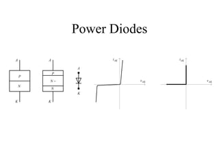
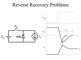
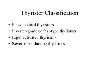
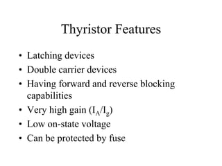
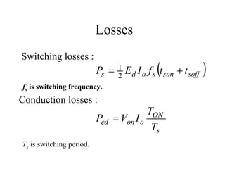
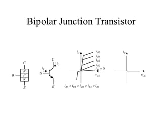
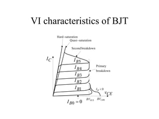
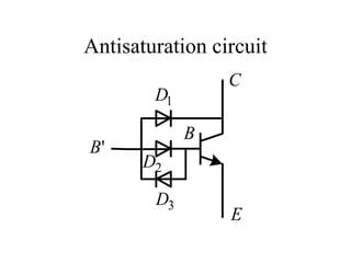
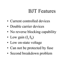
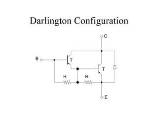
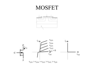
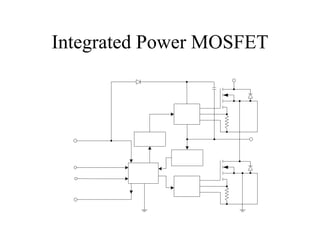
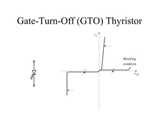
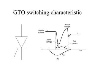
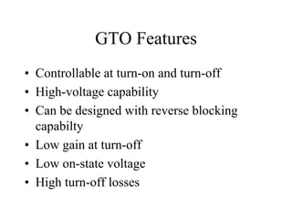
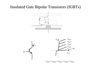
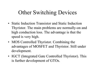
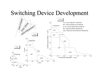
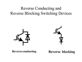
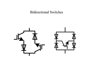
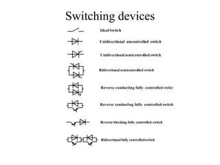
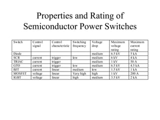
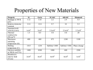
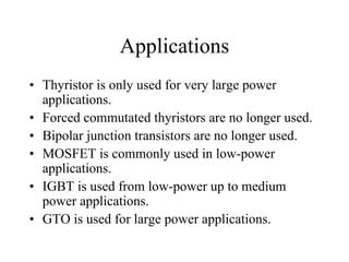
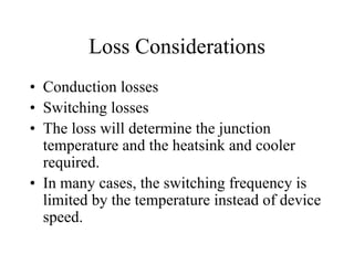
Power Semiconductor Switches

       Pekik Argo Dahono
Power Semiconductor Switches
• Diodes (Uncontrolled switches)
• Thyristors (Controllable at turn-on but
  uncontrolled at turn-off or commonly called
  as latched devices). Triac is under the same
  category.
• BJT, MOSFET, IGBT, GTO, MCT etc. are
  fully controllable switches.
Power Diodes

A       A             i AK          i AK

                A
            P
    P
        N−                   v AK          v AK
    N
            N
                K

K       K
Reverse Recovery Problems

                     VFD


      S
                            t rr
                     I FD

Ed    FD        Io


                      IS
                                   Io
Power diodes
Diodes are classified as:
- general purpose or line-frequency diodes
- Fast recovery diodes
- Schottky diodes
Schottky Diode
• The schottky diode has a smaller voltage
  drop compared to conventional diodes
  (about 0.3 V).
• The schottky diode has a smaller voltage
  breakdown than conventional diodes (less
  than 200 V).
Sample of diodes
Thyristor
    A                    iA

        iA


    P


    N
                              v AK
G   P


    N


    K
Thyristor Model
             I A = I E1
   I B1
             Q1
                           I C1 = −α1I E1 + I C 01
                           I C 2 = −α 2 I E 2 + I C 02
IC 2                I C1
                      IG        α 2 I G + I C 01 + I C 02
                           IA =
        Q2                          1 − (α1 + α 2 )
             I B2
       IE2
Thyristor Classification
•   Phase control thyristors
•   Inverter-grade or fast-type thyristors
•   Light activated thyristors
•   Reverse conducting thyristors
Thyristor Features
• Latching devices
• Double carrier devices
• Having forward and reverse blocking
  capabilities
• Very high gain (IA/Ig)
• Low on-state voltage
• Can be protected by fuse
Sample of thyristors
Thyristor Modules
Snubbers for Diodes and Thyristors

• Maximum dv/dt across diodes or thyristors
  must be limited and can be done by using an
  RC snubber that is connected in parallel to
  the devices.
• Maximum di/dt through diodes or thyristors
  must be limited and can be done by using an
  inductor that is connected in series to the
  devices.
Switching Characteristics

                         Gate
                         signal

                                              vT
                                                                iT
               Io    Transistor
                     voltage &    Ed                             Io
Ed   iT              current
                                  tdon                                tdoff
          vT                                            t fv                             t fi
                                    t ri   t son = tri + t fv              trv t
                                                                                 soff = t rv + t fi
                                                                1                                        1
                    Transistor                      Wson =        Ed I ot son                  Wsoff =     Ed I ot soff
                                                                2                                        2
                    power

                                                                          Pcd
Desired Switch Characteristics
•   Small leakage current in the off state
•   Small on-state voltage
•   Short turn-on and turn-off times
•   Large forward and reverse blocking voltage capabilities
•   High on-state current rating
•   Positive temperature coefficient of on-state resistance
•   Small control power
•   Wide Safe Operating Area
•   Large dv/dt and di/dt ratings
Safe Operating Area
i
     turn - on
                 turn - off


                              v
Losses
Switching losses :
                                             (
                          Ps = 1 E d I o f s t son + t soff
                               2
                                                              )
fs is switching frequency.
Conduction losses :
                                        TON
                          Pcd = Von I o
                                         Ts
Ts is switching period.
Bipolar Junction Transistor

                                     iC               iB 5     iC
                                                      iB 4
                 C                                    iB 3
    C                iC                               iB 2
            iB                                       iB1 = 0
    N
           B                                         vCE            vCE
B   P
    N

                 E        iB 5 > iB 4 > iB 3 > iB 2 > iB1
    E
VI characteristics of BJT
         Hard - saturation
                    Quasi - saturation

                     Second breakdown


    IC                 I B5
                                         Primary
                       I B4
                                         breakdown
                        I B3
                       I B2
                        I B1             IB < 0
                                                  vCE
                                 BVSUS   BVCB 0
                 I B0 = 0
Operating region
• Hard-saturation provides low voltage-drop but a
  large storage time (turn-off time)
• Quasi-saturation provides high voltage-drop but a
  small storage time.
• Second breakdown must be avoided by using a
  snubber and proper base current control.
• Negative base current results in higher voltage
  breakdown.
Antisaturation circuit
                 C
        D1

             B
B'
       D2

        D3
                 E
BJT Features
•   Current controlled devices
•   Double carrier devices
•   No reverse blocking capability
•   Low gain (Ic/Ib)
•   Low on-state voltage
•   Can not be protected by fuse
•   Second breakdown problem
Darlington Configuration
MOSFET


                       iD             vGS 5         iD
                                      vGS 4
    D                                 vGS 3
        iD                             vGS 2
                                      vGS1 = 0
G                                    vDS                 v DS

    S
             vGS 5 > vGS 4 > vGS 3 > vGS 2 > vGS1
MOSFET Features
•   Voltage controlled devices
•   Single carrier devices
•   High on-state voltage
•   Very high gain
•   No reverse blocking capability
•   No second breakdown problem
•   Can not be protected by fuse
Integrated Power MOSFET
Gate-Turn-Off (GTO) Thyristor
                 iA


                        Blocking
                        condition

                               v AK
GTO switching characteristic
                                      Anode
                                      voltage

          Anode     IA
          current                                     Vd


                     Spike
                    voltage                      Tail
                                                current


              0
                                                           Time


                                    IGR

                              (b)
GTO Features
• Controllable at turn-on and turn-off
• High-voltage capability
• Can be designed with reverse blocking
  capabilty
• Low gain at turn-off
• Low on-state voltage
• High turn-off losses
Insulated Gate Bipolar Transistors (IGBTs)


                                iC            vGE 5
            C                                 vGE 4
                iC                            vGE 3
                                              vGE 2
                                              vGE1 = 0
       G                                      vCE

            E
                     vGE5 > vGE 4 > vGE3 > vGE 2 > vGE1
IGBT Features
• Combining the advantages of BJT and
  MOSFET
• No reverse blocking capability
• No second breakdown
• High gain at turn on and turn off
Other Switching Devices
• Static Induction Transistor and Static Induction
  Thyristor. The main problems are normally-on and
  high conduction loss. The advantage is that the
  speed is very high.
• MOS Controlled Thyristor. Combining the
  advantages of MOSFET and Thyristor. Still under
  development.
• IGCT (Integrated Gate Controlled Thyristor). This
  is further development of GTOs.
Switching Device Development
                                ER
                                                                                                                                  2000
                             POW
                                                                                                                105                         GTO : GATE TURN-OFF THYRISTOR


                                                  E
                                                IV
                                      DR                                                                                                    MCT : MOS CONTROLLED THYRISTOR
                                                                                                                          THYRISTOR
                               H


                                                         Y                                                                                  SI Thy : STATIC INDUCTION THYRISTOR
                                                       NC
                           HIG


                                                     E
                                     SY


                                                                                                                                            BPT : BIPOLAR POWER TRANSISTOR
                                                   QU                                                           104
                                   EA


                                                                                                                          GTO
                                                  E


                                                                                           P (kVA)
                                                                                                                                            IGBT : INSULATED GATE BIPOLAR TRANSISTOR
                                                FR
                                      G   H
                                   HI                               1990
                                                                                                                          MCT         SI Thy


                                                                                           CONTROLLABLE POWER
                                                                                                                103

                                                104
                                                            THYRISTOR                                                                          IGBT
                                                                                                                102

                                                103         GTO
                    1980
                                                                                                                                  BPT
                                      P (kVA)


                                                                                                                101
                                                102
                                                                            IGBT
                                                                                                                                                      MOS
          104
                THYRISTOR                                     BPT
                                                101                                                             10-1 -1
          103                                                                                                      10           100         101       102         104         105      106
P (kVA)


                                                                                                                                      OPERATION FREQUENCY f (kHz)
                 GTO                                                               MOS
          102
                                                     -1
                                                10
                                                     10-1         100      101       102   104                            105
          101   BPT                                                          f (kHz)
          10-1 -1
             10      100     101   102           104
                           f (kHz)
Reverse Conducting and
Reverse Blocking Switching Devices


Reverse conducting   Reverse blocking
Bidirectional Switches
Switching devices
      Ideal Switch

      Unidirectional uncontrolled switch


      Unidirectional semicontrolled switch


      Bidirectional semicontrolled switch


       Reverse conducting fully controlled switch


      Reverse conducting fully controlled switch


      Reverse blocking fully controlled switch


       Bidirectional fully controlled switch
Properties and Rating of
         Semiconductor Power Switches
Switch     Control   Control          Switching   Voltage   Maximum   Maximum
           signal    characteristic   frequency   drop      voltage   current
                                                            rating    rating
Diode                                             medium    6.5 kV    5 kA
SCR        current   trigger          low         medium    6 kV      4 kA
TRIAC      current   trigger                      medium    1 kV      50 A
GTO        current   trigger          low         medium    6.5 kV    4.5 kA
BJT        current   linear           medium      low       1.5 kV    1 kA
MOSFET     voltage   linear           Very high   high      1 kV      200 A
IGBT       voltage   linear           high        medium    3.5 kV    2 kA
Properties of New Materials
Property               Si     GaAs      3C-SiC         6H-SiC        Diamond
Bandgap at 300 K      1.12    1.43        2.2            2.9            5.5
(eV)
Relative dielectric   11.8    12.8        9.7            10             5.5
constant
Saturated drift
velocity (cm/s)       1x10⁷   2x10⁷     2.5x10⁷        2.5x10⁷        2.7x10⁷
Thermal                1.5     0.5        5.0            5.0             20
conductivity
(W/cm/o C
Maximum               400     460         873           1240           1100
operating
temperature (K)
Melting               1415    1238    Sublime>1800   Sublime>1800   Phase change
temperature (C)
Electron mobility     1400    8500       1000            600           2200
at 300 K (cm2 /Vs)
Breakdown
electric field        3x10⁵   4x10⁵      4x10⁶          4x10⁶          1x10⁷
(V/cm)
Applications
• Thyristor is only used for very large power
  applications.
• Forced commutated thyristors are no longer used.
• Bipolar junction transistors are no longer used.
• MOSFET is commonly used in low-power
  applications.
• IGBT is used from low-power up to medium
  power applications.
• GTO is used for large power applications.
Loss Considerations
• Conduction losses
• Switching losses
• The loss will determine the junction
  temperature and the heatsink and cooler
  required.
• In many cases, the switching frequency is
  limited by the temperature instead of device
  speed.
Snubbers
• Turn-off losses can be reduced by using a turn-off
  snubber. This snubber is also useful to limit high
  dv/dt across the device.
• Turn-on losses can be reduced by using a turn-on
  snubber. This snubber is also useful to limit high
  di/dt through the device.
• Snubbers are useful to reduce the switching losses
  on the switching devices. The total switching
  losses, however, may still the same or even
  increase.
Turn-ON and turn-OFF Snubbers
Reducing Switching Losses
• Switching losses can be reduced by using lossless
  snubbers. These snubbers, however, may make the
  converter circuit became complicated.
• IGBTs may operate without snubbers.
• GTOs and IGCTs usually need a turn-off snubber
  because of high tail current.
• Switching losses can be reduced or even
  eliminated by using soft-switching techniques.
  These methods, however, may increase the
  required voltage and/or current ratings.

Elektronika daya kuliah ke 2

  • 1.
  • 2.
    Power Semiconductor Switches •Diodes (Uncontrolled switches) • Thyristors (Controllable at turn-on but uncontrolled at turn-off or commonly called as latched devices). Triac is under the same category. • BJT, MOSFET, IGBT, GTO, MCT etc. are fully controllable switches.
  • 3.
    Power Diodes A A i AK i AK A P P N− v AK v AK N N K K K
  • 4.
    Reverse Recovery Problems VFD S t rr I FD Ed FD Io IS Io
  • 5.
    Power diodes Diodes areclassified as: - general purpose or line-frequency diodes - Fast recovery diodes - Schottky diodes
  • 6.
    Schottky Diode • Theschottky diode has a smaller voltage drop compared to conventional diodes (about 0.3 V). • The schottky diode has a smaller voltage breakdown than conventional diodes (less than 200 V).
  • 7.
  • 8.
    Thyristor A iA iA P N v AK G P N K
  • 9.
    Thyristor Model I A = I E1 I B1 Q1 I C1 = −α1I E1 + I C 01 I C 2 = −α 2 I E 2 + I C 02 IC 2 I C1 IG α 2 I G + I C 01 + I C 02 IA = Q2 1 − (α1 + α 2 ) I B2 IE2
  • 10.
    Thyristor Classification • Phase control thyristors • Inverter-grade or fast-type thyristors • Light activated thyristors • Reverse conducting thyristors
  • 11.
    Thyristor Features • Latchingdevices • Double carrier devices • Having forward and reverse blocking capabilities • Very high gain (IA/Ig) • Low on-state voltage • Can be protected by fuse
  • 12.
  • 13.
  • 14.
    Snubbers for Diodesand Thyristors • Maximum dv/dt across diodes or thyristors must be limited and can be done by using an RC snubber that is connected in parallel to the devices. • Maximum di/dt through diodes or thyristors must be limited and can be done by using an inductor that is connected in series to the devices.
  • 15.
    Switching Characteristics Gate signal vT iT Io Transistor voltage & Ed Io Ed iT current tdon tdoff vT t fv t fi t ri t son = tri + t fv trv t soff = t rv + t fi 1 1 Transistor Wson = Ed I ot son Wsoff = Ed I ot soff 2 2 power Pcd
  • 16.
    Desired Switch Characteristics • Small leakage current in the off state • Small on-state voltage • Short turn-on and turn-off times • Large forward and reverse blocking voltage capabilities • High on-state current rating • Positive temperature coefficient of on-state resistance • Small control power • Wide Safe Operating Area • Large dv/dt and di/dt ratings
  • 17.
    Safe Operating Area i turn - on turn - off v
  • 18.
    Losses Switching losses : ( Ps = 1 E d I o f s t son + t soff 2 ) fs is switching frequency. Conduction losses : TON Pcd = Von I o Ts Ts is switching period.
  • 19.
    Bipolar Junction Transistor iC iB 5 iC iB 4 C iB 3 C iC iB 2 iB iB1 = 0 N B vCE vCE B P N E iB 5 > iB 4 > iB 3 > iB 2 > iB1 E
  • 20.
    VI characteristics ofBJT Hard - saturation Quasi - saturation Second breakdown IC I B5 Primary I B4 breakdown I B3 I B2 I B1 IB < 0 vCE BVSUS BVCB 0 I B0 = 0
  • 21.
    Operating region • Hard-saturationprovides low voltage-drop but a large storage time (turn-off time) • Quasi-saturation provides high voltage-drop but a small storage time. • Second breakdown must be avoided by using a snubber and proper base current control. • Negative base current results in higher voltage breakdown.
  • 22.
    Antisaturation circuit C D1 B B' D2 D3 E
  • 23.
    BJT Features • Current controlled devices • Double carrier devices • No reverse blocking capability • Low gain (Ic/Ib) • Low on-state voltage • Can not be protected by fuse • Second breakdown problem
  • 24.
  • 25.
    MOSFET iD vGS 5 iD vGS 4 D vGS 3 iD vGS 2 vGS1 = 0 G vDS v DS S vGS 5 > vGS 4 > vGS 3 > vGS 2 > vGS1
  • 26.
    MOSFET Features • Voltage controlled devices • Single carrier devices • High on-state voltage • Very high gain • No reverse blocking capability • No second breakdown problem • Can not be protected by fuse
  • 27.
  • 28.
    Gate-Turn-Off (GTO) Thyristor iA Blocking condition v AK
  • 29.
    GTO switching characteristic Anode voltage Anode IA current Vd Spike voltage Tail current 0 Time IGR (b)
  • 30.
    GTO Features • Controllableat turn-on and turn-off • High-voltage capability • Can be designed with reverse blocking capabilty • Low gain at turn-off • Low on-state voltage • High turn-off losses
  • 31.
    Insulated Gate BipolarTransistors (IGBTs) iC vGE 5 C vGE 4 iC vGE 3 vGE 2 vGE1 = 0 G vCE E vGE5 > vGE 4 > vGE3 > vGE 2 > vGE1
  • 32.
    IGBT Features • Combiningthe advantages of BJT and MOSFET • No reverse blocking capability • No second breakdown • High gain at turn on and turn off
  • 33.
    Other Switching Devices •Static Induction Transistor and Static Induction Thyristor. The main problems are normally-on and high conduction loss. The advantage is that the speed is very high. • MOS Controlled Thyristor. Combining the advantages of MOSFET and Thyristor. Still under development. • IGCT (Integrated Gate Controlled Thyristor). This is further development of GTOs.
  • 34.
    Switching Device Development ER 2000 POW 105 GTO : GATE TURN-OFF THYRISTOR E IV DR MCT : MOS CONTROLLED THYRISTOR THYRISTOR H Y SI Thy : STATIC INDUCTION THYRISTOR NC HIG E SY BPT : BIPOLAR POWER TRANSISTOR QU 104 EA GTO E P (kVA) IGBT : INSULATED GATE BIPOLAR TRANSISTOR FR G H HI 1990 MCT SI Thy CONTROLLABLE POWER 103 104 THYRISTOR IGBT 102 103 GTO 1980 BPT P (kVA) 101 102 IGBT MOS 104 THYRISTOR BPT 101 10-1 -1 103 10 100 101 102 104 105 106 P (kVA) OPERATION FREQUENCY f (kHz) GTO MOS 102 -1 10 10-1 100 101 102 104 105 101 BPT f (kHz) 10-1 -1 10 100 101 102 104 f (kHz)
  • 35.
    Reverse Conducting and ReverseBlocking Switching Devices Reverse conducting Reverse blocking
  • 36.
  • 37.
    Switching devices Ideal Switch Unidirectional uncontrolled switch Unidirectional semicontrolled switch Bidirectional semicontrolled switch Reverse conducting fully controlled switch Reverse conducting fully controlled switch Reverse blocking fully controlled switch Bidirectional fully controlled switch
  • 38.
    Properties and Ratingof Semiconductor Power Switches Switch Control Control Switching Voltage Maximum Maximum signal characteristic frequency drop voltage current rating rating Diode medium 6.5 kV 5 kA SCR current trigger low medium 6 kV 4 kA TRIAC current trigger medium 1 kV 50 A GTO current trigger low medium 6.5 kV 4.5 kA BJT current linear medium low 1.5 kV 1 kA MOSFET voltage linear Very high high 1 kV 200 A IGBT voltage linear high medium 3.5 kV 2 kA
  • 39.
    Properties of NewMaterials Property Si GaAs 3C-SiC 6H-SiC Diamond Bandgap at 300 K 1.12 1.43 2.2 2.9 5.5 (eV) Relative dielectric 11.8 12.8 9.7 10 5.5 constant Saturated drift velocity (cm/s) 1x10⁷ 2x10⁷ 2.5x10⁷ 2.5x10⁷ 2.7x10⁷ Thermal 1.5 0.5 5.0 5.0 20 conductivity (W/cm/o C Maximum 400 460 873 1240 1100 operating temperature (K) Melting 1415 1238 Sublime>1800 Sublime>1800 Phase change temperature (C) Electron mobility 1400 8500 1000 600 2200 at 300 K (cm2 /Vs) Breakdown electric field 3x10⁵ 4x10⁵ 4x10⁶ 4x10⁶ 1x10⁷ (V/cm)
  • 40.
    Applications • Thyristor isonly used for very large power applications. • Forced commutated thyristors are no longer used. • Bipolar junction transistors are no longer used. • MOSFET is commonly used in low-power applications. • IGBT is used from low-power up to medium power applications. • GTO is used for large power applications.
  • 41.
    Loss Considerations • Conductionlosses • Switching losses • The loss will determine the junction temperature and the heatsink and cooler required. • In many cases, the switching frequency is limited by the temperature instead of device speed.
  • 42.
    Snubbers • Turn-off lossescan be reduced by using a turn-off snubber. This snubber is also useful to limit high dv/dt across the device. • Turn-on losses can be reduced by using a turn-on snubber. This snubber is also useful to limit high di/dt through the device. • Snubbers are useful to reduce the switching losses on the switching devices. The total switching losses, however, may still the same or even increase.
  • 43.
  • 44.
    Reducing Switching Losses •Switching losses can be reduced by using lossless snubbers. These snubbers, however, may make the converter circuit became complicated. • IGBTs may operate without snubbers. • GTOs and IGCTs usually need a turn-off snubber because of high tail current. • Switching losses can be reduced or even eliminated by using soft-switching techniques. These methods, however, may increase the required voltage and/or current ratings.