A novel approach for designing Ultra Low Power and wide dynamic range circuit for multiplexing analog
signals is presented. The design operates in weak inversion (Sub threshold) region and uses Source -
Coupled Logic ( SCL) circuit. The bias current of the SCL gates is varied to scale down linearly the power
consumption and the operating frequency. The multiplexer design employs CMOS transistors as
transmission gate with dynamic threshold voltage. The design exhibits low power dissipation, high
dynamic range and good linearity. The design was implemented in 180 nm technology and was operated at
a supply voltage of 400 mV with a bias current ranging in the order of few Pico-amperes. The ON and
OFF resistance of the transmission gate achieved were 27 ohms and 10 M ohms respectively. The power
dissipation achieved is around 0.79 μW for a dynamic range of 1μV to 0.4 V.
A low power cmos analog circuit design for acquiring multichannel eeg signalsVLSICS Design
EEG signals are the signatures of neural activities and are captured by multiple-electrodes and the signals are recorded from pairs of electrodes. To acquire these multichannel signals a low power CMOS circuit was designed and implemented. The design operates in weak inversion region employing sub threshold
source coupled logic. A 16 channel differential multiplexer is designed by utilizing a transmission gate with
dynamic threshold logic and a 4 to 16 decoder is used to select the individual channels. The ON and OFF
resistance of the transmission gate obtained is 27 ohms and 10 M ohms respectively. The power dissipation
achieved is around 337nW for a dynamic range of 1μV to 0.4 V.
Compact low power high slew-rate cmos buffer amplifier with power gating tech...VLSICS Design
A qualitative analysis of different parameters such as Phase noise, Slew rate and tranconductance by using
power gating reduction technique is presented. The circuit achieves the large driving capability by
employing simple comparators to sense the transients of the input to turn on the output stages, which are
statically off in the stable state. The effect of the different number of transistors and their topologies on the
phase noise and Slew rate is analyzed. Good agreement between qualitative and quantitative measurements
is observed. Scope of reducing of Noise and avoidance of Leakage due to various sources is discussed.
Study and Review on Various Current Comparatorsijsrd.com
This paper presents study and review on various current comparators. It also describes low voltage current comparator using flipped voltage follower (FVF) to obtain the single supply voltage. This circuit has short propagation delay and occupies a small chip area as compare to other current comparators. The results of this circuit has obtained using PSpice simulator for 0.18 μm CMOS technology and a comparison has been performed with its non FVF counterpart to contrast its effectiveness, simplicity, compactness and low power consumption.
Analysis and Design of CMOS Source Followers and Super Source FollowerIDES Editor
The source follower circuit is used as a voltage
buffer and level shifter. It is more flexible level shifter as the
dc value of voltage level can be adjusted by changing aspect
ratio of MOSFETs. It is desired to have low output resistance
for such applications. Source follower can give minimum
output resistance 1/(gm+gmb) with load resistance and channel
resistance tending to infinity. The super source follower is a
circuit formed using negative feedback through another
MOSFET. This offers even reduced output resistance but with
reduced voltage gain as that of source follower.
Design of 64 bit SRAM using Lector Technique for Low Leakage Power with Read ...IOSRJVSP
: In complementary metal oxide semiconductor (CMOS) the power dissipation predominantly comprises of dynamic as well as static power. Prior to introduction of “Deep submicron technologies” it is observed that in case of technology process with feature size larger than 1micro meter, the consumption of dynamic power out of the overall power consumption of any circuit is more than 90%,while that of static power is negligible. But in the present deep submicron technologies in order to, reduce the dynamic power consumption in VLSI circuits, the power supply is being scaled down, keeping in view the principle that the dynamic power dissipated is directly proportional to the square of the supply voltage (Vdd).The threshold voltage also needs to be reduced since the supply voltage is scaled down. Overcoming the inherent limitations in the existing method for leakage power reduction, The Lector (Leakage controlled transistor) technique which works efficiently both in active and idle states of the circuit and results in better leakage power reduction is now proposed. The proposed system presents the analysis of power on “64-bit SRAM array using leakage controlled transistor technique
Design and Control of Switched-Inductor Quasi-Z-Source Inverter for Photovolt...irjes
The conventional Z-Source Inverter (ZSI) used for photovoltaic applications has certain
shortcomings such as high stress across the passive components and low boost factor. This paper presents the
design and analysis of three phase switched inductor quasi Z-source inverter (SL-QZSI) for photovoltaic (PV)
applications. The wide voltage gain and the compensation for dead time effect of SL-QZSI with the help of
shoot-through states makes it suitable for PV application. Modulation strategies such as Simple boost,
Maximum boost and Constant maximum boost control methods are investigated for the operation and control
of SL-QZSI. PV source is modeled in MATLAB and incremental & conductance MPPT algorithm is
implemented .Simulation of the SL-QZSI circuit powered by PV source is carried out by implementing
maximum boost control method and the performance parameters are discussed.
Improved Trans-Z-source Inverter for Automobile ApplicationIJTET Journal
In this paper a new technology is proposed with a replacement of conventional voltage source/current
source inverter with Improved Trans-Z-source inverter in automobile applications. The improved Trans-Z-source
inverter has a high boost inversion capability and continues input current. Also this new inverter can suppress the
resonant current at the startup; this resonant current in the startup may lead the device to permanent damage. In
improved Trans-Z-source inverter a couple inductor is needed, instead of this coupled inductor a transformer is used.
By using a transformer with sufficient turns ratio the size can be reduced. The turn’s ratio of the transformer decides
the input voltage of the inverter. In this paper operating principle, comparison with conventional inverters, working
with automobiles simulation results, THD analysis, Hardware implementation using ATMEGA 328 P are included.
Space Vector of Three Phase Three level Neutral Point Clamped Quasi Z Source ...IJTET Journal
Space vector of three phase three level neutral point clamped quasi z source inverter is proposed in this paper. Space vector modulation is the pulse width modulation consists of number of switching states. Space vector pulse width modulation technique utilizes 15% more power from DC source. Harmonics are reduced by the presence of switching states. Quasi Z-source inverter is advanced topologies which performs both boost and buck operation of a converter. The proposed inverter obtains continuous input current and the boost converter is not needed. So, maximum voltage can be obtained in the load and system complexity is reduced. Maximum power can be obtained from the solar panel by using MPPT. The implementation of MPPT is to operate a PV array under constant voltage and power reference to modify the duty cycle of the inverter.The simulation of proposed topology is done in MATLAB/SIMULINK software.
Power quality improvement using impedance network based invertereSAT Publishing House
IJRET : International Journal of Research in Engineering and Technology is an international peer reviewed, online journal published by eSAT Publishing House for the enhancement of research in various disciplines of Engineering and Technology. The aim and scope of the journal is to provide an academic medium and an important reference for the advancement and dissemination of research results that support high-level learning, teaching and research in the fields of Engineering and Technology. We bring together Scientists, Academician, Field Engineers, Scholars and Students of related fields of Engineering and Technology.
Application of PWM Control Strategy on Z-Source Isolated Dual active bridge D...IJMER
This project presents a Z-source with bidirectional dc–dc converter. The switching count is
reduced by adding a passive element. Thus, we are improving the output voltage level. The voltage
regulation range of proposed converter is better than that of the traditional bidirectional dc–dc
converter. The fully bridge symmetrical circuit configuration, is neither a high-voltage side nor a lowvoltage
side in the circuit structure, and the sources connected to the dc side of each H-bridge circuit
with voltage sources and current sources. This method can reduce current stress and improves the
system efficiency.
In this paper we are presenting a dual active bridge (DAB) dc–dc converter is also known as
Bidirectional DC-DC converter. Both simulation results are shown by using MATLAB software.
A three level quasi-two-stage single-phase pfc converter with flexible output...LeMeniz Infotech
A three level quasi-two-stage single-phase pfc converter with flexible output voltage and improved conversion efficiency
To Get this projects Call : 9566355386 / 99625 88976
Visit : www.lemenizinfotech.com / www.ieeemaster.com
Mail : projects@lemenizinfotech.com
Now day’s the power factor has become a major problem in power system to improve the power quality of the grid, as power factor is affected on the grid due to the nonlinear loads connected to it. Single phase bridgeless AC/DC power factor correction (PFC) topology to improve the power factor as well as the total harmonic distortion (THD) of the utility grid is proposed. By removing the input bridge in conventional PFC converters, the control circuit is simplified; the total harmonics distortion (THD) and power factor (PF) are improved. The PI controller operates in two loops one is the outer control loop which calculates the reference current through LC filter and signal processing. Inner current loop generates PWM switching signals through the PI controller. The output of the proposed PFC topology is verified for prototype using MATLAB circuit simulations. The experimental system is developed, and the simulation results are obtained.
A unity power factor bridgeless isolated cuk converter fed brushless dc motor...LeMeniz Infotech
A unity power factor bridgeless isolated cuk converter fed brushless dc motor drive
To Get this projects Call : 9566355386 / 99625 88976
Visit : www.lemenizinfotech.com / www.ieeemaster.com
Mail : projects@lemenizinfotech.com
Review of Integrated Power Factor Correction (PFC) Boost converter topologies...IJARBEST JOURNAL
This paper provides a review of various Power Factor Correction (PFC) boost
converter topologies suitable for telecoms. A novel integrated PFC topology is proposed which acts
as a backup power supply for telecommunication systems. The advantage of the proposed circuit is
that it operates based on soft switching principle thereby reducing the switching losses in the
converter. The topologies analyzed in this paper are conventional average current mode control
boost PFC, bridgeless boost PFC, semi-bridgeless boost PFC, totem-pole bridgeless boost PFC and
proposed integrated boost PFC. All these topology studies are investigated by carrying out the
simulation of the converter circuits using PSIM software. A detailed comparison of all the
topologies have been done and they are compared in terms of supply power factor, supply current
THD and displacement factor. From the results, it is inferred that the proposed integrated PFC
provides a reduced supply current THD and improved power factor. The results are validated.
Design of ultra low power 8 channel analog multiplexer using dynamic threshol...VLSICS Design
The design of an ultra low voltage, low power high
speed 8 channel Analog multiplexer in 180nm CMOS
technology is presented. A modified transmission ga
te using a dynamic threshold voltage MOSFET
(DTMOS
)
is employed in the design. The design is optimized
with respect to critical requirements like short
switching time, low power dissipation, good lineari
ty and high dynamic range with an operating voltage
of
0.4V. The ON and OFF resistances achieved are 32 oh
ms and 10Mohms respectively with a switching
speed of 10MHz. The power dissipation obtained is a
round 2.65uW for a dynamic range of 1uV to 0.4V.
DESIGN OF A PROGRAMMABLE LOW POWER LOW DROP-OUT REGULATORVLSICS Design
A low power programmable low drop-out regulator capable of providing 1V output has been proposed. The
regulator requires a supply voltage of 1.2V and works in the temperature range of -40 to 125 °C in nominal
corner (i.e, normal doping for PMOS and NMOS Field Effect Transistors), yielding a load regulation of
3%. The output voltage level is controlled externally by means of 2 1-bit control signals. The circuit
provides a DC gain of 30 dB and a maximum DC Power Supply Rejection Ratio of -35 dB and a worst case
PSRR of -20 dB. Power dissipation in the load is nearly 100 μW
SINGLE-PORT FIVE-TRANSISTOR SRAM CELL WITH REDUCED LEAKAGE CURRENT IN STANDBYVLSICS Design
In this paper, a new single-port five-transistor (5T) Static Random Access Memory (SRAM) cell with
integrated read/write assist is proposed. Amongst the assist circuitry, a voltage control circuit is coupled to
the sources corresponding to driver transistors of each row memory cells. This configuration is aimed to
control the source voltages of driver transistors under different operating modes. Specifically, during a
write operation, by means of sizing the driver transistor close to bitline to resolve the write ‘1’ issue. In
addition, associated with a two-stage reading mechanism to increase the reading speed and to avoid
unnecessary power consumption. Finally, with the standby start-up cir
Designing High-Speed, Low-Power Full Adder Cells Based on Carbon Nanotube Tec...VLSICS Design
This article presents novel high speed and low power full adder cells based on carbon nanotube field effect
transistor (CNFET). Four full adder cells are proposed in this article. First one (named CN9P4G) and
second one (CN9P8GBUFF) utilizes 13 and 17 CNFETs respectively. Third design that we named
CN10PFS uses only 10 transistors and is full swing. Finally, CN8P10G uses 18 transistors and divided into
two modules, causing Sum and Cout signals are produced in a parallel manner. All inputs have been used
straight, without inverting. These designs also used the special feature of CNFET that is controlling the
threshold voltage by adjusting the diameters of CNFETs to achieve the best performance and right voltage
levels. All simulation performed using Synopsys HSPICE software and the proposed designs are compared
to other classical and modern CMOS and CNFET-based full adder cells in terms of delay, power
consumption and power delay product.
Vlsics040303LOW POWER DUAL EDGE - TRIGGERED STATIC D FLIP-FLOPVLSICS Design
This paper enumerates new architecture of low power dual-edge triggered Flip-Flop (DETFF) designed at
180nm CMOS technology. In DETFF same data throughput can be achieved with half of the clock
frequency as compared to single edge triggered Flip-Flop (SETFF). In this paper conventional and
proposed DETFF are presented and compared at same simulation conditions. The post layout experimental
results comparison shows that the average power dissipation is improved by 48.17%, 41.29% and 36.84%
when compared with SCDFF, DEPFF and SEDNIFF respectively and improvement in PDP is 42.44%,
33.88% and 24.69% as compared to SCDFF, DEPFF and SEDNIFF respectively. Therefore the proposed
DETFF design is suitable for low power and small area applications
Design of low power cmos logic circuits using gate diffusion input (gdi) tech...VLSICS Design
The Gate diffusion input (GDI) is a novel technique
for low power digital circuit design. This techniq
ue
reduces the power dissipation, propagation delay, a
rea of digital circuits and it maintains low comple
xity
of logic design. In this paper, the 4×1 Multiplexer
, 8×3 Encoder, BCD Counter and Mealy State Machine
were implemented by using Pass Transistors (PT), Tr
ansmission Gate (TG) and Gate Diffusion Input (GDI)
technique and then they were compared with each oth
er for power dissipation. The Multiplexers and
Encoders are combinational circuits and Counters an
d mealy machines are sequential circuits both of th
em
are very important digital systems so power optimiz
ation should be done to those digital circuits. The
whole processes for development of digital circuits
and simulation was done by using the mentor graphi
cs
backend tool. This method can also be extended to t
he processors and other high level designs for
optimization of power dissipation, area and delay i
n order to increase the circuit efficiency.
LEAKAGE REDUCTION TECHNIQUE AND ANALYSIS OF CMOS D FLIP FLOPVLSICS Design
The expansion of battery operated portable device is continuously increasing the demand for low
power, minimum delay and high speed integrated circuits. In many of the portable devices the
standby periods are longer than the active periods and thus consume more power in the standby
state [2]. It is extremely important to reduce the power consumption in the standby mode. In
today’s high performance integrated circuits the leakage power contributes major power
consumption than overall total power consumption. In deep submicron circuits the leakage
power increases than the dynamic power and also in the circuits when there are no transitions at
the input and the transistors are in steady state [1]. Leakage power is mainly due to leakage
current that flows in the circuit when the circuit is operated in sleep or standby mode. The
leakage current is composed of sub-threshold leakage current, gate current, gate leakage current
and reverses biased leakage. Among all leakages, sub-threshold leakage contributes major part of
the leakage. The sub-threshold leakage current of a metal oxide semiconductor device is
expressed as
Where µo is the mobility of electrons/holes, Cox denotes oxide
capacitance of gate per unit area, W and L are width and channel length of MOS device
respectively, Vgs is the gate to source voltage Vt is the thermal voltage and η is the swing
coefficient. The contents of this paper are organized as follows: Section 2 descr
Multisim design and simulation of 2.2 g hz lna for wireless communicationVLSICS Design
This paper presents the work done on the design and simulation of a high frequency low noise amplifier for
wireless communication. The purpose of the amplifier is to amplify the received RF path of a wireless
network. With high gain, high sensitivity and low noise using Bipolar Junction transistor (BJT). The design
methodology requires analysis of the transistor for stability, proper matching, network selection and
fabrication. The BJT transistor was chosen for the design of the LNA due to its low noise and good gain at
high frequency. These properties were confirmed using some measurement techniques including Network
Analyzer, frequency analyzer Probe and Oscilloscope for the simulation and practical testing of the
amplifier to verify the performance of the designed High frequency Low noise amplifier. The design goals
of noise figure of 0.52dB-0.7dB and bias conditions are Vcc = 3.5 V and Icc= 55 mA to produce 16.8 dB
gain across the 0.4–2.2GHz band.
Evolution of Structure of Some Binary Group-Based N-Bit Compartor, N-To-2N De...VLSICS Design
Reversible logic has attracted substantial interest due to its low power consumption which is the main
concern of low power VLSI systems. In this paper, a novel 4x4 reversible gate called inventive gate has
been introduced and using this gate 1-bit, 2-bit, 8-bit, 32-bit and n-bit group-based reversible comparator
have been constructed with low value of reversible parameters. The MOS transistor realizations of 1-bit, 2-
bit, and 8-bit of reversible comparator are also presented and finding power, delay and power delay
product (PDP) with appropriate aspect ratio W/L. Novel inventive gate has the ability to use as an n-to-2n
decoder. Different novel reversible circuit design style is compared with the existing ones. The relative
results shows that the novel reversible gate wide utility, group-based reversible comparator outperforms
the present style in terms of number of gates, garbage outputs and constant input.
MINIMALLY BUFFERED ROUTER USING WEIGHTED DEFLECTION ROUTING FOR MESH NETWORK ...VLSICS Design
The scalability, modularity and massive parallelism exhibited by Network on chip(NoC) interconnects
make them highly suitable for the inter core communication framework of multiprocessor system-on-chip
(MPSoC) designs. Routers play the most vital role in transferring flits through the network, hence efficient
microarchitecture and cost effective routing algorithms are highly essential for modern NoC routers.
Elimination of buffers and deflection routing help to achieve energy and area efficiency of these routers.
The advantages of bufferless and buffered designs can be combined by using a minimum number of side
buffers to store a fraction of deflection flits in the router. In this paper, we propose a routing algorithm
based on weighted deflection of flits for minimally buffered deflection routers. Evaluations on 4x4 and 8x8
mesh NoC using synthetic workloads as well as benchmark applications demonstrate that deflection rate
and average network latency are significantly reduced in comparison with the state of the art NoC routers.
Performance analysis of the newly proposed algorithm shows that the network saturation point improves
by 26% compared to earlier designs in this domain
Impact of parameter variations and optimization on dg pnin tunnel fetVLSICS Design
The downscaling of conventional MOSFETs has come to its fundamental limits. TFETs are very attractive
devices for low power applications because of their low off-current and potential for smaller sub threshold
slope. In this paper, the impact of various parameter variations on the performance of a DG-PNIN Tunnel
field effect transistor is investigated. In this work, variations in gate oxide material, source doping, channel
doping, drain doping, pocket doping and body thickness are studied and all these parameters are optimized
as performance boosters to give better current characteristics parameters. After optimization with all these
performance boosters, the device has shown improved performance with increased on-current and reduced
threshold voltage and the Ion/Ioff ratio is > 106.
Optimal Unate Decomposition Method for Synthesis of Mixed CMOS VLSI CircuitsVLSICS Design
Static CMOS logic style is often the choice of designers for synthesizing low power circuits. This style is
robust in terms of noise integrity however, it offers less speed. Domino logic style, as an alternative is often
found in critical paths of various large scale high performance circuits. Yet, due to high switching activity
they are not suitable for synthesis of low power circuits. To achieve both power and speed benefits, we
propose a method of designing circuit using mixed CMOS logic style, taking advantages of both static and
Domino logic styles. For a given circuit, we extract the unate and binate components using a unate
decomposition algorithm. These are optimized such that the resulting circuit is optimum in terms of power,
area and delay. To do this, a multi-objective genetic algorithm is employed. The optimized unate and binate
blocks are mapped using Domino and static cell libraries, respectively. Testing the efficacy of our
approach with ISCAS85 and MCNC89 benchmark circuits showed an improvement of 25% in delay and
22% in transistor count with 12% more power dissipation compared to circuits with only static CMOS
logic. Thus, mixed CMOS circuits are promising in high speed and area constraint applications.
A RAIL-TO-RAIL HIGH SPEED CLASS-AB CMOS BUFFER WITH LOW POWER AND ENHANCED SL...VLSICS Design
A rail-to-rail class-AB CMOS buffer is proposed in this paper to drive large capacitive loads. A new
technique is used to reduce the leakage power of class-AB CMOS buffer circuits without affecting dynamic
power dissipation .The name of applied technique is LECTOR, which gives the high speed buffer with the
reduced low power dissipation (1.05%) and reduced area (2.8%). The proposed buffer is simulated at
45nm CMOS technology and the circuit is operated at 3V supply with cadence software. This analog circuit
is performed with extremely low leakage current as well as high current driving capability for the large
input voltages. The proposed paper is achieved very high speed with very low propagation delay range
i.e.(292×10-12). So the delay of the circuit is reduced to 10%. The settling time of this circuit is reduced by
24% (in ns) at 3V square wave input. The measured quiescent current is 41μA
FGMOS BASED LOW-VOLTAGE LOW-POWER HIGH OUTPUT IMPEDANCE REGULATED CASCODE CUR...VLSICS Design
Floating Gate MOS (FGMOS) transistors can be very well implemented in lieu of conventional MOSFET
for design of a low-voltage, low-power current mirror. Incredible features of flexibility, controllability and
tunability of FGMOS yields better results with respect to power, supply voltage and output swing. This
paper presents a new current mirror designed with FGMOS which exhibit high output impedance, higher
current range, very low power dissipation and higher matching accuracy. It achieves current range of up to
1500 µA, high output impedance of 1.125 TΩ, bandwidth of 4.1 MHz and dissipates power as low as 10.56
µW. The proposed design has been simulated using Cadence Design Environment in 180 nm CMOS
process technology with +1.0 Volt single power supply
SMART MULTICROSSBAR ROUTER DESIGN IN NOCVLSICS Design
This paper gives the innovative idea of designing a router using multicrossbar switch in Network on
Chip(NoC) . In Network-on-Chip architectures the input buffer can consume a large portion of the total
power. Eliminating all input buffer would result in increased power consumption at high load, while
reducing the size of input buffer degrades the performance. In this paper we have proposed a muticrossbar
router design using elastic buffer by combining the advantage of both buffered and buffer less network. In
the proposed design Power Delay Product is reduced by around 37 .91% as compared to baseline router
DESIGN OF IMPROVED RESISTOR LESS 45NM SWITCHED INVERTER SCHEME (SIS) ANALOG T...VLSICS Design
This work presents three different approaches which eliminates the resistor ladder completely and hence
reduce the power demand drastically of a Analog to Digital Converter. The first approach is Switched
Inverter Scheme (SIS) ADC; The test result obtained for it on 45nm technology indicates an offset error of
0.014 LSB. The full scale error is of -0.112LSB. The gain error is of 0.07 LSB, actual full scale range of
0.49V, worst case DNL & INL each of -0.3V. The power dissipation for the SIS ADC is 207.987 μwatts;
Power delay product (PDP) is 415.9 fWs, and the area is 1.89μm2. The second and third approaches are
clocked SIS ADC and Sleep transistor SIS ADC. Both of them show significant improvement in power
dissipation as 57.5% & 71% respectively. Whereas PDP is 229.7 fWs and area is 0.05 μm2 for Clocked SIS
ADC and 107.3 fWs & 1.94 μm2 for Sleep transistor SIS ADC.
Energy Efficient Design of Multiplexer Using Adiabatic logicIJEEE
the increasing prominence of portable systems and the need to limit the power consumption in very high density VLSI chips have led to rapid and innovative developments in low power design during the recent years. The CMOS technology provides circuits with very low static power dissipation, during the switching operation currents are generated, due to the discharge of load capacitances that cause power dissipation increasing with the clock frequency. The adiabatic technique prevents such losses, the charge does not flow from the supply voltage to the load capacitance and then to ground, but it flows back to a trapezoidal or sinusoidal supply voltage and can be reused.In this paper a low 2:1 multiplexer is designed using positive feedback adiabatic logic. The design is simulated at .12µm technology using Microwind 3.1. Simulated results shows that proposed design saves 38% energy as compare to conventional CMOS design.
NOVEL SLEEP TRANSISTOR TECHNIQUES FOR LOW LEAKAGE POWER PERIPHERAL CIRCUITSVLSICS Design
Static power consumption is a major concern in nanometre technologies. Along with technology scaling down and higher operating speeds of CMOS VLSI circuits, the leakage power is getting enhanced. As process geometries are becoming smaller, device density increases and threshold voltage as well as oxide thickness decrease to keep pace with performance. Two novel circuit techniques for leakage current reduction in inverters with and without state retention property are presented in this work. The power dissipation during inactive (standby) mode of operation can be significantly reduced compared to traditional power gating methods by these circuit techniques. The proposed circuit techniques are applied to inverters and the results are compared with earlier inverter leakage minimization techniques. Inverter
buffer chains are designed using new state retention low leakage technique and found to be dissipating lower power with state retention. All low leakage inverters are designed and simulated in cadence design environment using 90 nm technology files. The leakage power during sleep mode is found to be better by X 63 times for novel method. The total power dissipation has also reduced by a factor of X 3.5, compared to earlier sleepy keeper technique. The state retention feature is also good compared to earlier leakage power reduction methodologies.
Sub-Threshold Leakage Current Reduction Techniques In VLSI Circuits -A SurveyIJERA Editor
There is an increasing demand for portable devices powered up by battery, this led the manufacturers of
semiconductor technology to scale down the feature size which results in reduction in threshold voltage and
enables the complex functionality on a single chip. By scaling down the feature size the dynamic power
dissipation has no effect but the static power dissipation has become equal or more than that of Dynamic power
dissipation. So in recent CMOS technologies static power dissipation i.e. power dissipation due to leakage
current has become a challenging area for VLSI chip designers. In order to prolong the battery life and maintain
reliability of circuit, leakage current reduction is the primary goal. A basic overview of techniques used for
reduction of sub-threshold leakages is discussed in this paper. Based on the surveyed techniques, one would be
able to choose required and apt leakage reduction technique.
FORCED STACK SLEEP TRANSISTOR (FORTRAN): A NEW LEAKAGE CURRENT REDUCTION APPR...VIT-AP University
Reduction in leakage current has become a significant concern in nanotechnology-based low-power, low-voltage, and high-performance VLSI applications. This research article discusses a new low-power circuit design the approach of FORTRAN (FORced stack sleep TRANsistor), which decreases the leakage power efficiency in the CMOS-based circuit outline in VLSI domain. FORTRAN approach reduces leakage current in both active as well as standby modes of operation. Furthermore, it is not time intensive when the circuit goes from active mode to standby mode and vice-versa. To validate the proposed design approach, experiments are conducted in the Tanner EDA tool of mentor graphics bundle on projected circuit designs for the full adder, a chain of 4-inverters, and 4-bit multiplier designs utilizing 180nm, 130nm, and 90nm TSMC technology node. The outcomes obtained show the result of a 95-98% vital reduction in leakage power as well as a 15-20% reduction in dynamic power with a minor increase in delay. The result outcomes are compared for accuracy with the notable design approaches that are accessible for both active and standby modes of operation.
IEEE JOURNAL OF SOLID-STATE CIRCUITS, VOL. 32, NO. 7, JULY 199MalikPinckney86
IEEE JOURNAL OF SOLID-STATE CIRCUITS, VOL. 32, NO. 7, JULY 1997 1079
Low-Power Logic Styles: CMOS
Versus Pass-Transistor Logic
Reto Zimmermann and Wolfgang Fichtner,Fellow, IEEE
Abstract—Recently reported logic style comparisons based on
full-adder circuits claimed complementary pass-transistor logic
(CPL) to be much more power-efficient than complementary
CMOS. However, new comparisons performed on more efficient
CMOS circuit realizations and a wider range of different logic
cells, as well as the use of realistic circuit arrangements demon-
strate CMOS to be superior to CPL in most cases with respect
to speed, area, power dissipation, and power-delay products.
An implemented 32-b adder using complementary CMOS has
a power-delay product of less than half that of the CPL version.
Robustness with respect to voltage scaling and transistor sizing,
as well as generality and ease-of-use, are additional advantages
of CMOS logic gates, especially when cell-based design and logic
synthesis are targeted. This paper shows that complementary
CMOS is the logic style of choice for the implementation of
arbitrary combinational circuits if low voltage, low power, and
small power-delay products are of concern.
Index Terms—Adder circuits, CPL, complementary CMOS,
low-voltage low-power logic styles, pass-transistor logic, VLSI
circuit design.
I. I NTRODUCTION
T HE increasing demand for low-power very large scaleintegration (VLSI) can be addressed at different de-
sign levels, such as the architectural, circuit, layout, and
the process technology level [1]. At the circuit design level,
considerable potential for power savings exists by means of
proper choice of a logic style for implementing combinational
circuits. This is because all the important parameters governing
power dissipation—switching capacitance, transition activity,
and short-circuit currents—are strongly influenced by the
chosen logic style. Depending on the application, the kind
of circuit to be implemented, and the design technique used,
different performance aspects become important, disallowing
the formulation of universal rules for optimal logic styles. In-
vestigations of low-power logic styles reported in the literature
so far, however, have mainly focused on particular logic cells,
namely full-adders, used in some arithmetic circuits. In this
paper, these investigations are extended to a much wider set of
logic gates, and with that, to arbitrary combinational circuits.
The power dissipation characteristics of various existing logic
styles are compared qualitatively and quantitatively by actual
logic gate implementations and simulations under realistic cir-
cuit arrangements and operating conditions [2]. Investigations
of sequential elements, such as latches and flip-flops, were
Manuscript received November 20, 1996; revised January 29, 1997.
The authors are with the Integrated Systems Laboratory, Swiss Federal
Institute of Technology (ETH), CH-8092 Zurich, Switzerland.
Publisher It ...
A COMPARATIVE STUDY OF ULTRA-LOW VOLTAGE DIGITAL CIRCUIT DESIGNVLSICS Design
Ultra-low voltage digital circuit design is an active research area, especially for portable applications such as wearable electronics, intelligent remote sensors, implantable medical devices, and energy-harvesting systems. Due to their application scenarios and circuit components, two major goals for these systems are minimizing energy consumption and improving compatibility with low-voltage power supplies and analog components. The most effective solution to achieve these goals is to reduce the supply voltage, which, however, raises the issue of operability. At ultra-low supply voltages, the integrity of digital signals degrades dramatically due to the indifference between active and leakage currents. In addition, the system timing becomes more unpredictable as the impact of process and supply voltage variations being more significant at lower voltages. This paper presents a comparative study among three techniques for designing digital circuits operating at ultra-low voltages, i.e., Schmitt-triggered gate structure, delayinsensitive asynchronous logic, and Fully-Depleted Silicon-on-Insulator technology. Results show that despite the tradeoffs, all eight combinations of these techniques are viable for designing ultra-low voltage circuits. For a given application, the optimum circuit design can be selected from these combinations based on the lowest voltage, the dynamic range, the power budget, the performance requirement, and the available semiconductor process node.
A new improved mcml logic for dpa resistant circuitsVLSICS Design
Security of electronic data remains the major conce
rn. The art of encryption to secure the data can be
achieved in various levels of abstraction. The choi
ce of the logic style in implementing the security
algorithms has greater significance, and it can enh
ance the ability of providing better resistance to
side
channel attacks. The static CMOS logic style is pro
ved to be prone to side channel power attacks. The
exploration of CMOS current mode logic style for re
sistance against these side channel attacks is disc
ussed
in this paper. Various characteristics of the curre
nt mode logic styles, which make it suitable for ma
king
DPA resistant circuits are explored. A new methodol
ogy of biasing the sleep transistors of (MOS curren
t
mode logic) MCML families is proposed. It uses pass
gate transistors for power-gating the circuits. Th
e
power variations of the proposed circuits are compa
red against the standard CMOS counterparts. Logic
gates such as XOR, NAND and AND gate structures of
MCML families and static CMOS are designed and
compared for the ability of side channel resistance
. A distributed arrangement of sleep transistors fo
r
reducing the static power dissipation in the logic
gates is also proposed, designed and analyzed. All
the
logic gates in MCML and CMOS were implemented using
standard 180 nm CMOS technology employing
Cadence® EDA tools.
Back track input vector algorithm for leakage reduction in cmos vlsi digital ...VLSICS Design
A new algorithm based on Input Vector Control (IVC) technique is proposed, which shifts logic gate of a
circuit to its minimum leakage state, when device goes into its idle state. Leakage current in CMOS VLSI
circuit has become a major constrain in a battery operated device for technology node below 90nm, as it
drains the battery even when a circuit is in standby mode. Major concern is the leakage even in run time
condition, here aim is to focus on run time leakage reduction technique of integrated Circuit. It is inherited
by stacking effect when the series transistors are maximized in OFF state condition. This method is
independent of process technology and does not require any additional power supply. This paper gives an
optimized solution of input pattern determination of some small circuit to find minimum leakage vector
considering promising and non-promising node which helps to reduce the time complexity of the algorithm.
Proposed algorithm is simulated using HSPICE simulator for 2 input NAND gate and different standard
logic cells and achieved 94.2% and 54.59 % average leakage power reduction for 2 input NAND cell and
different logics respectively.
A DAPTIVE S UPPLY V OLTAGE M ANAGEMENT F OR L OW P OWER L OGIC C IRCU...VLSICS Design
With the rise in demand of portable hand held devic
es and with the rise in application of wireless sen
sor
networks and RFID reduction of total power consumpt
ion has become a necessity. To save power we
operate the logic circuitry of our devices at sub-t
hreshold. In sub-threshold the drain current is
exponentially dependent on the threshold voltage he
nce the threshold variation causes profound variati
on
of I
ON
and I
OFF
the ratio of which affect the speed of a circuit d
rastically. So to mitigate this problem we
present a adaptive power management circuit which w
ill determine the minimum required supply voltage
to meet the timing requirement. Also to reduce the
power overhead and avoid bulky coil and EMI noise
we used the switch capacitor power regulator to reg
ulate and manage power instead of linear dropout
(LDO) and Inductor base switch mode power converter
A Bus Encoding Method for Crosstalk and Power Reduction in RC Coupled VLSI In...VLSICS Design
The performance factors such as propagation delay, power dissipation and crosstalk in RC modelled interconnects are major design issues for the System on-chip (SoC) designs in current Deep Submicron (DSM) era. The crosstalk effect is a consequence of coupling and switching activities that is encountered when there is a transition as compared to previous state of wire and or when there are transitions in adjacent wires. Therefore, minimization or elimination of switching and coupling activities is crucial in enhancing the performance of SoC designs. There are several methods for the reduction of power dissipation, crosstalk and delay. The encoding method is most effective and popular method for enhancing the behaviour of on-chip buses. This paper proposes encoding scheme to achieve overall reduction in transitions. The reduction in transition improves the performance in terms of reduced power dissipation, coupling activity and delay in on-chip buses. This encoding method is implemented using VHDL. The result evidently demonstrates reduction in transitions which consequently improves the overall performance of on-chip buses.
A low power front end analog multiplexing unit for 12 lead ecg signal acquisi...VLSICS Design
The design of CMOS analog circuitry for acquiring 12 lead ECG is presented. The existing methods
employ separate multiplexers and associated circuitry for signal acquisition operating at typical voltage of
± 5V. The proposed system employs dynamic threshold logic to achieve low power, wide dynamic range
good linearity with a supply voltage of 0.4V. The power dissipation obtained was 22.12μW. Utilizing the
dynamic threshold logic the proposed circuitry is implemented with 0.18μm CMOS technology. This ECG
signal processor is highly suitable for wearable applications of long term cardiac monitoring.
International Journal of Engineering Research and Applications (IJERA) is an open access online peer reviewed international journal that publishes research and review articles in the fields of Computer Science, Neural Networks, Electrical Engineering, Software Engineering, Information Technology, Mechanical Engineering, Chemical Engineering, Plastic Engineering, Food Technology, Textile Engineering, Nano Technology & science, Power Electronics, Electronics & Communication Engineering, Computational mathematics, Image processing, Civil Engineering, Structural Engineering, Environmental Engineering, VLSI Testing & Low Power VLSI Design etc.
ANALYSIS OF CMOS AND MTCMOS CIRCUITS USING 250 NANO METER TECHNOLOGYcscpconf
The low-power consumption with less delay time has become an important issue in the recent
trends of VLSI. In these days, the low power systems with high speed are highly preferable
everywhere. Designers need to understand how low-power techniques affect performance
attributes, and have to choose a set of techniques that are consistent with these attributes .The
main objective of this paper is to describe, how to achieve low power consumption with
approximately same delay time in a single circuit. In this paper, we make circuits with CMOS
and MTCMOS techniques and check out its power and delay characteristics. The circuits
designed using MTCMOS technique gives least power consumption.
All the pre-layout simulations have been performed at 250nm technology on tanner EDA tool.
Analysis of CMOS and MTCMOS Circuits Using 250 Nano Meter Technology csandit
The low-power consumption with less delay time has become an important issue in the recent
trends of VLSI. In these days, the low power systems with high speed are highly preferable
everywhere. Designers need to understand how low-power techniques affect performance
attributes, and have to choose a set of techniques that are consistent with these attributes .The
main objective of this paper is to describe, how to achieve low power consumption with
approximately same delay time in a single circuit. In this paper, we make circuits with CMOS
and MTCMOS techniques and check out its power and delay characteristics. The circuits
designed using MTCMOS technique gives least power consumption.
All the pre-layout simulations have been performed at 250nm technology on tanner EDA tool.
IJCER (www.ijceronline.com) International Journal of computational Engineerin...ijceronline
Call for paper 2012, hard copy of Certificate, research paper publishing, where to publish research paper,
journal publishing, how to publish research paper, Call For research paper, international journal, publishing a paper, IJCER, journal of science and technology, how to get a research paper published, publishing a paper, publishing of journal, publishing of research paper, research and review articles, IJCER Journal, How to publish your research paper, publish research paper, open access engineering journal, Engineering journal, Mathematics journal, Physics journal, Chemistry journal, Computer Engineering, Computer Science journal, how to submit your paper, peer review journal, indexed journal, research and review articles, engineering journal, www.ijceronline.com, research journals,
yahoo journals, bing journals, International Journal of Computational Engineering Research, Google journals, hard copy of Certificate,
journal of engineering, online Submission
International Journal of Engineering Research and Applications (IJERA) is an open access online peer reviewed international journal that publishes research and review articles in the fields of Computer Science, Neural Networks, Electrical Engineering, Software Engineering, Information Technology, Mechanical Engineering, Chemical Engineering, Plastic Engineering, Food Technology, Textile Engineering, Nano Technology & science, Power Electronics, Electronics & Communication Engineering, Computational mathematics, Image processing, Civil Engineering, Structural Engineering, Environmental Engineering, VLSI Testing & Low Power VLSI Design etc.
Similar to A Sub Threshold Source Coupled Logic Based Design of Low Power CMOS Analog Multiplexer (20)
Courier management system project report.pdfKamal Acharya
It is now-a-days very important for the people to send or receive articles like imported furniture, electronic items, gifts, business goods and the like. People depend vastly on different transport systems which mostly use the manual way of receiving and delivering the articles. There is no way to track the articles till they are received and there is no way to let the customer know what happened in transit, once he booked some articles. In such a situation, we need a system which completely computerizes the cargo activities including time to time tracking of the articles sent. This need is fulfilled by Courier Management System software which is online software for the cargo management people that enables them to receive the goods from a source and send them to a required destination and track their status from time to time.
NO1 Uk best vashikaran specialist in delhi vashikaran baba near me online vas...Amil Baba Dawood bangali
Contact with Dawood Bhai Just call on +92322-6382012 and we'll help you. We'll solve all your problems within 12 to 24 hours and with 101% guarantee and with astrology systematic. If you want to take any personal or professional advice then also you can call us on +92322-6382012 , ONLINE LOVE PROBLEM & Other all types of Daily Life Problem's.Then CALL or WHATSAPP us on +92322-6382012 and Get all these problems solutions here by Amil Baba DAWOOD BANGALI
#vashikaranspecialist #astrologer #palmistry #amliyaat #taweez #manpasandshadi #horoscope #spiritual #lovelife #lovespell #marriagespell#aamilbabainpakistan #amilbabainkarachi #powerfullblackmagicspell #kalajadumantarspecialist #realamilbaba #AmilbabainPakistan #astrologerincanada #astrologerindubai #lovespellsmaster #kalajaduspecialist #lovespellsthatwork #aamilbabainlahore#blackmagicformarriage #aamilbaba #kalajadu #kalailam #taweez #wazifaexpert #jadumantar #vashikaranspecialist #astrologer #palmistry #amliyaat #taweez #manpasandshadi #horoscope #spiritual #lovelife #lovespell #marriagespell#aamilbabainpakistan #amilbabainkarachi #powerfullblackmagicspell #kalajadumantarspecialist #realamilbaba #AmilbabainPakistan #astrologerincanada #astrologerindubai #lovespellsmaster #kalajaduspecialist #lovespellsthatwork #aamilbabainlahore #blackmagicforlove #blackmagicformarriage #aamilbaba #kalajadu #kalailam #taweez #wazifaexpert #jadumantar #vashikaranspecialist #astrologer #palmistry #amliyaat #taweez #manpasandshadi #horoscope #spiritual #lovelife #lovespell #marriagespell#aamilbabainpakistan #amilbabainkarachi #powerfullblackmagicspell #kalajadumantarspecialist #realamilbaba #AmilbabainPakistan #astrologerincanada #astrologerindubai #lovespellsmaster #kalajaduspecialist #lovespellsthatwork #aamilbabainlahore #Amilbabainuk #amilbabainspain #amilbabaindubai #Amilbabainnorway #amilbabainkrachi #amilbabainlahore #amilbabaingujranwalan #amilbabainislamabad
Explore the innovative world of trenchless pipe repair with our comprehensive guide, "The Benefits and Techniques of Trenchless Pipe Repair." This document delves into the modern methods of repairing underground pipes without the need for extensive excavation, highlighting the numerous advantages and the latest techniques used in the industry.
Learn about the cost savings, reduced environmental impact, and minimal disruption associated with trenchless technology. Discover detailed explanations of popular techniques such as pipe bursting, cured-in-place pipe (CIPP) lining, and directional drilling. Understand how these methods can be applied to various types of infrastructure, from residential plumbing to large-scale municipal systems.
Ideal for homeowners, contractors, engineers, and anyone interested in modern plumbing solutions, this guide provides valuable insights into why trenchless pipe repair is becoming the preferred choice for pipe rehabilitation. Stay informed about the latest advancements and best practices in the field.
Democratizing Fuzzing at Scale by Abhishek Aryaabh.arya
Presented at NUS: Fuzzing and Software Security Summer School 2024
This keynote talks about the democratization of fuzzing at scale, highlighting the collaboration between open source communities, academia, and industry to advance the field of fuzzing. It delves into the history of fuzzing, the development of scalable fuzzing platforms, and the empowerment of community-driven research. The talk will further discuss recent advancements leveraging AI/ML and offer insights into the future evolution of the fuzzing landscape.
Event Management System Vb Net Project Report.pdfKamal Acharya
In present era, the scopes of information technology growing with a very fast .We do not see any are untouched from this industry. The scope of information technology has become wider includes: Business and industry. Household Business, Communication, Education, Entertainment, Science, Medicine, Engineering, Distance Learning, Weather Forecasting. Carrier Searching and so on.
My project named “Event Management System” is software that store and maintained all events coordinated in college. It also helpful to print related reports. My project will help to record the events coordinated by faculties with their Name, Event subject, date & details in an efficient & effective ways.
In my system we have to make a system by which a user can record all events coordinated by a particular faculty. In our proposed system some more featured are added which differs it from the existing system such as security.
Welcome to WIPAC Monthly the magazine brought to you by the LinkedIn Group Water Industry Process Automation & Control.
In this month's edition, along with this month's industry news to celebrate the 13 years since the group was created we have articles including
A case study of the used of Advanced Process Control at the Wastewater Treatment works at Lleida in Spain
A look back on an article on smart wastewater networks in order to see how the industry has measured up in the interim around the adoption of Digital Transformation in the Water Industry.
About
Indigenized remote control interface card suitable for MAFI system CCR equipment. Compatible for IDM8000 CCR. Backplane mounted serial and TCP/Ethernet communication module for CCR remote access. IDM 8000 CCR remote control on serial and TCP protocol.
• Remote control: Parallel or serial interface.
• Compatible with MAFI CCR system.
• Compatible with IDM8000 CCR.
• Compatible with Backplane mount serial communication.
• Compatible with commercial and Defence aviation CCR system.
• Remote control system for accessing CCR and allied system over serial or TCP.
• Indigenized local Support/presence in India.
• Easy in configuration using DIP switches.
Technical Specifications
Indigenized remote control interface card suitable for MAFI system CCR equipment. Compatible for IDM8000 CCR. Backplane mounted serial and TCP/Ethernet communication module for CCR remote access. IDM 8000 CCR remote control on serial and TCP protocol.
Key Features
Indigenized remote control interface card suitable for MAFI system CCR equipment. Compatible for IDM8000 CCR. Backplane mounted serial and TCP/Ethernet communication module for CCR remote access. IDM 8000 CCR remote control on serial and TCP protocol.
• Remote control: Parallel or serial interface
• Compatible with MAFI CCR system
• Copatiable with IDM8000 CCR
• Compatible with Backplane mount serial communication.
• Compatible with commercial and Defence aviation CCR system.
• Remote control system for accessing CCR and allied system over serial or TCP.
• Indigenized local Support/presence in India.
Application
• Remote control: Parallel or serial interface.
• Compatible with MAFI CCR system.
• Compatible with IDM8000 CCR.
• Compatible with Backplane mount serial communication.
• Compatible with commercial and Defence aviation CCR system.
• Remote control system for accessing CCR and allied system over serial or TCP.
• Indigenized local Support/presence in India.
• Easy in configuration using DIP switches.
Industrial Training at Shahjalal Fertilizer Company Limited (SFCL)MdTanvirMahtab2
This presentation is about the working procedure of Shahjalal Fertilizer Company Limited (SFCL). A Govt. owned Company of Bangladesh Chemical Industries Corporation under Ministry of Industries.
Immunizing Image Classifiers Against Localized Adversary Attacksgerogepatton
This paper addresses the vulnerability of deep learning models, particularly convolutional neural networks
(CNN)s, to adversarial attacks and presents a proactive training technique designed to counter them. We
introduce a novel volumization algorithm, which transforms 2D images into 3D volumetric representations.
When combined with 3D convolution and deep curriculum learning optimization (CLO), itsignificantly improves
the immunity of models against localized universal attacks by up to 40%. We evaluate our proposed approach
using contemporary CNN architectures and the modified Canadian Institute for Advanced Research (CIFAR-10
and CIFAR-100) and ImageNet Large Scale Visual Recognition Challenge (ILSVRC12) datasets, showcasing
accuracy improvements over previous techniques. The results indicate that the combination of the volumetric
input and curriculum learning holds significant promise for mitigating adversarial attacks without necessitating
adversary training.
Gen AI Study Jams _ For the GDSC Leads in India.pdf
A Sub Threshold Source Coupled Logic Based Design of Low Power CMOS Analog Multiplexer
1. International Journal of VLSI design & Communication Systems (VLSICS) Vol.5, No.5, October 2014
A SUB THRESHOLD SOURCE COUPLED LOGIC
BASED DESIGN OF LOW POWER CMOS
ANALOG MULTIPLEXER
G.Deepika1, P.Rama Krishna2 and Dr.K.S.Rao3
2,3Department of Electronics and Communication Engineering,
ANURAG Group of Institutions, Hyderabad, India
1Department of Electronics and Communication Engineering,
RRS College of Engineeering & Technology, Hyderabad, India
ABSTRACT
A novel approach for designing Ultra Low Power and wide dynamic range circuit for multiplexing analog
signals is presented. The design operates in weak inversion (Sub threshold) region and uses Source -
Coupled Logic ( SCL) circuit. The bias current of the SCL gates is varied to scale down linearly the power
consumption and the operating frequency. The multiplexer design employs CMOS transistors as
transmission gate with dynamic threshold voltage. The design exhibits low power dissipation, high
dynamic range and good linearity. The design was implemented in 180 nm technology and was operated at
a supply voltage of 400 mV with a bias current ranging in the order of few Pico-amperes. The ON and
OFF resistance of the transmission gate achieved were 27 ohms and 10 M ohms respectively. The power
dissipation achieved is around 0.79 μW for a dynamic range of 1μV to 0.4 V.
KEYWORDS
Low Power, Source Coupled Logic, Sub threshold, Multiplexer, Analog Signals.
1. INTRODUCTION
This work basically highlights on the applicability of sub-threshold source coupled logic
(STSCL) for building analog circuits and systems that run at very low voltage and obligation to
provide enticing performance with exquisite energy savings. Fields like bio-medical engineering
need very less energy consumption for long battery life. Besides meeting the ultra-low power
specification, the system must also be reliable and should function under harsh conditions. In this
work, logic gates are designed and analyzed using STSCL. These gates are used for
implementation of analog subsystems which would operate at very low supply voltages and
consume very less power.
The switch finds many applications in integrated circuit design. In analog circuits, the switch is
employed to implement useful areas like multiplexing, modulation and other applications. It is
used as a transmission gate in digital circuits and adds a dimension of flexibility as found in
standard logic circuits. The implementation of Ultra Low Power Systems has proved to the quite
DOI : 10.5121/vlsic.2014.5504 45
2. International Journal of VLSI design & Communication Systems (VLSICS) Vol.5, No.5, October 2014
pivoted in many modern applications in many areas like mobile systems [1],[2] , sensor
networks[3],[4], and implantable biomedical applications [5]. Low power has gained more
importance in today’s electronics industry. The Necessity for low power has caused a major
paradigm shift where power dissipation has become significant consideration in performance and
area wise.
CMOS switches have great characteristics and in its most important form, a voltage-controlled
resistor which offers very low resistance less than 100 in its ON state and very High resistance
of several hundreds of Mega ohms in OFF state with Pico-ampere leakage currents. CMOS
technology is compatible with logic circuitry and integrates large number of ICs. [6]. Its fast
switching characteristics are well controlled with minimum circuit leakage. MOSFET transistors
can switch positive and negative voltages and conduct positive and negative currents with equal
ease.
Implementation of high performance systems especially for low power applications creates many
challenges and requires the trade off among speed of operation, power consumption, supply
voltage and device parameters such as threshold voltage and oxide thickness in conventional
CMOS technology.
When the MOSFET is in sub threshold operation the trans conductance to bias current ratio of
the transistor is maximum and the current density is very low [7], [8]. On the other hand, for
implementing widely adjustable circuits the exponential relationship between drain current and
gate voltage makes this mode of operation well suited [7], [9]. The dynamic (switching) power
consumption which is quadratic ally dependent on the supply voltage will cause the CMOS logic
circuits utilizing sub threshold region transistors operate with a very low power consumption
[10]–[13]. Therefore reduction in supply voltage reduces power dissipation and also output
voltage swing [1], [14] thereby increasing the delay in each gate. This means the power
dissipation, logic swing, and speed of operation are related to each other. The control of power
consumption becomes difficult due to the exponential relation between power dissipation and
supply voltage in sub threshold region. To implement very low power systems it is necessary to
minimize the power dissipation at the system level in addition to the gate level for achieving
desired performance [10].
This paper presents a new topology for implementing analog switch for ultra low power
applications. For achieving this a novel approach for implementing Source Coupled Logic (
SCL) circuits biased in sub threshold region is described. The speed of operation is independent
of supply voltage and threshold voltage of devices. In addition the current consumption in each
cell can be brought down to few pico- Amperes. It is therefore possible to reduce the system
power consumption well below the sub threshold leakage current of conventional CMOS circuits.
To enable operation at very low current levels and to attain the desired performance
specifications, special circuit techniques have to be applied for implementing very low power
SCL circuits.
The work focuses on the technique for implementing sub threshold (STSCL) gates where the bias
current of each cell can be set as low as 10pA. A brief review of SCL circuits, the proposed
technique for implementing the low power analog switch using sub threshold SCL gates, power
consumption and experimental results are described in the following sections.
46
3. International Journal of VLSI design Communication Systems (VLSICS) Vol.5, No.5, October 2014
47
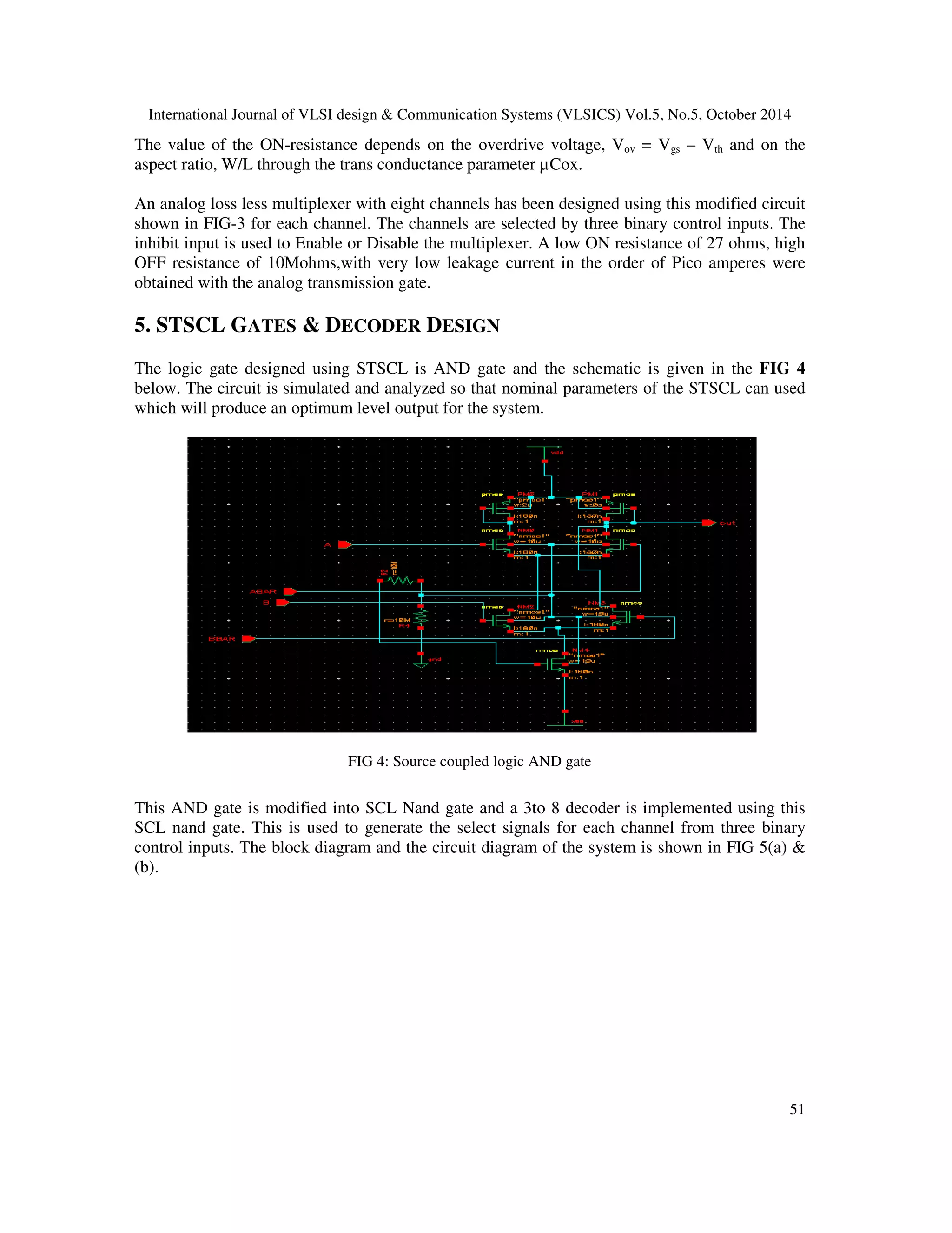
2. SUBTHRESHOLD SOURCE-COUPLED LOGIC CIRCUITS
The speed of operation in an SCL gate is inherently high as the logic operation mainly takes place
in current domain. An NMOS source coupled differential pair transistors acts as a switch to steer
the tail current Iss to one of the output depending on the input logic. The Load resistor RL
converts this current to output voltage to drive the other SCL gates. In order to switch the input
differential pair of the next stage the output voltage swing ( RL ISS ) should be adequately high.
Based on this the drain source over drive voltage input pair should be larger than 2 n Vdssat when
Vin = 0.
Fig. 1. Source Coupled Logic-based inverter/buffer circuit.
A source coupled logic based inverter/ buffer circuit is shown in FIG 1. More complex logic
functions can be implemented by using a complex network of NMOS source coupled pairs as
switching part [7,13]. The load resistance RL is implemented by biasing the PMOS device in
triode region and also NMOS switching network should be arranged in a proper way to achieve
desired logic operation. The input logic level steers the tail bias current into one of the branch of
the source coupled pair and this current is converted to voltage by the load resistance. The DC
response of the SCL circuit is given in FIG 2.
Operating In sub threshold region, the device trans conductance does not depend upon the device
size but strongly depends on the temperature through UT. Hence by changing the design
parameters it is not possible to change the transfer curve [12].
4. International Journal of VLSI design Communication Systems (VLSICS) Vol.5, No.5, October 2014
48
FIG 2. DC response of the SCL circuit.
The voltage swing and the current required for charging and discharging the parasitic
capacitances is less in SCL topology, when compared to the CMOS topology where the signal
swing is equal to VDD. The major advantage in SCL topology is reduction in signal swing. In
order to make the tail bias current completely switch to one of the two output branches, the
voltage swing at the input and output of a logic circuit should be high enough. The voltage swing
at the output node is given as
VSW = RL . ISS
should be adequately high to switch completely the input differential pair of the next stage. In
other words SCL circuit can be used as a logic circuit with allowable noise margin if its gain is
sufficiently high. The region of operation of the NMOS devices [17,18] gives the minimum
allowable voltage swing at the output of each SCL gate.
,= 2 ∙
9. is the subthreshold slope factor of NMOS devices. In the sub threshold region the
required voltage swing can be as low as 150 mV at room temperature (assuming ). This swing in
the sub threshold region depends on the sub threshold slope factor and is independent of the
threshold voltage of the NMOS switching devices.
A PMOS device is used as a load device when SCL gate is biased in sub threshold region as
shown in FIG 1. Since all the devices are operated in sub threshold region the tail bias current can
be reduced till comparable with leakage currents in the circuit.
The trans conductance of the input differential pair is given as
10. International Journal of VLSI design Communication Systems (VLSICS) Vol.5, No.5, October 2014
PMOS and NMOS Transistors can be combined as transmission gate for implementing analog
switch which selectively allows or blocks the signal from input to output. The transistors are
turned ON or OFF by applying control signals to the gates in complimentary manner and at the
output a drop in signal amplitude is observed. This problem is eliminated by modifying the
transmission gate by stacking transistors and the signal is passed to the output without any loss.
49
3. BODY BIASING
The voltage difference between the Transistors Source and the Bulk (VSB) will effect the change
in Transistor Threshold voltage VT. Since VSB effects VT the bulk can be treated as second Gate
that helps to identify how the transistor turns On and OFF.
Body effect refers to the change in the transistor threshold voltage (VT) resulting from a voltage
difference between the transistor source and body. Because the voltage difference between the
source and body affects the VT, the body can be thought of as a second gate that helps determine
how the transistor turns ON and OFF. The strength of the body effect is usually quantified by the
body coefficient g(gamma). The threshold voltage of MOSFET is well known as,
VTh = VTh0 + gB(Ö|2fF +VSB| - (Ö|2fF| )
where VSB is the voltage between source and bulk, fF is the bulk Fermi- potential ,VTh0 is the
threshold voltage when VSB=0 and g B is the body-effect coefficient. Therefore varying threshold
voltage Vth can be changed by varying VSB which can form dynamic threshold voltage MOSFET
(DTMOS). Normally, the source and body junction is either zero-biased or reverse-biased.
Forward-body-biased MOSFETs can also be used on some circuit to improve performance with
lower threshold voltage VTh [10]. This concept is utilized in designing the power analog
multiplexer. The transistors are operated in strong inversion region by means of using 0.4 V
forward body bias.
Varieties of body biasing techniques are enabled by strong body effect and these techniques are
effectively utilized in older generation. This body bias can be applied externally (external to the
chip) or internally (in chip). The internal approach normally utilizes a charge pump circuit
provide reverse body bias or potential divider to produce forward body bias. Reverse body bias
for an n channel transistors increases the threshold voltage and makes the transistors both slow
and less leakage. On the other hand forward body bias reduces the threshold voltage making the
transistor fast and with more leakage. The polarities of the body bias are opposite for P channel
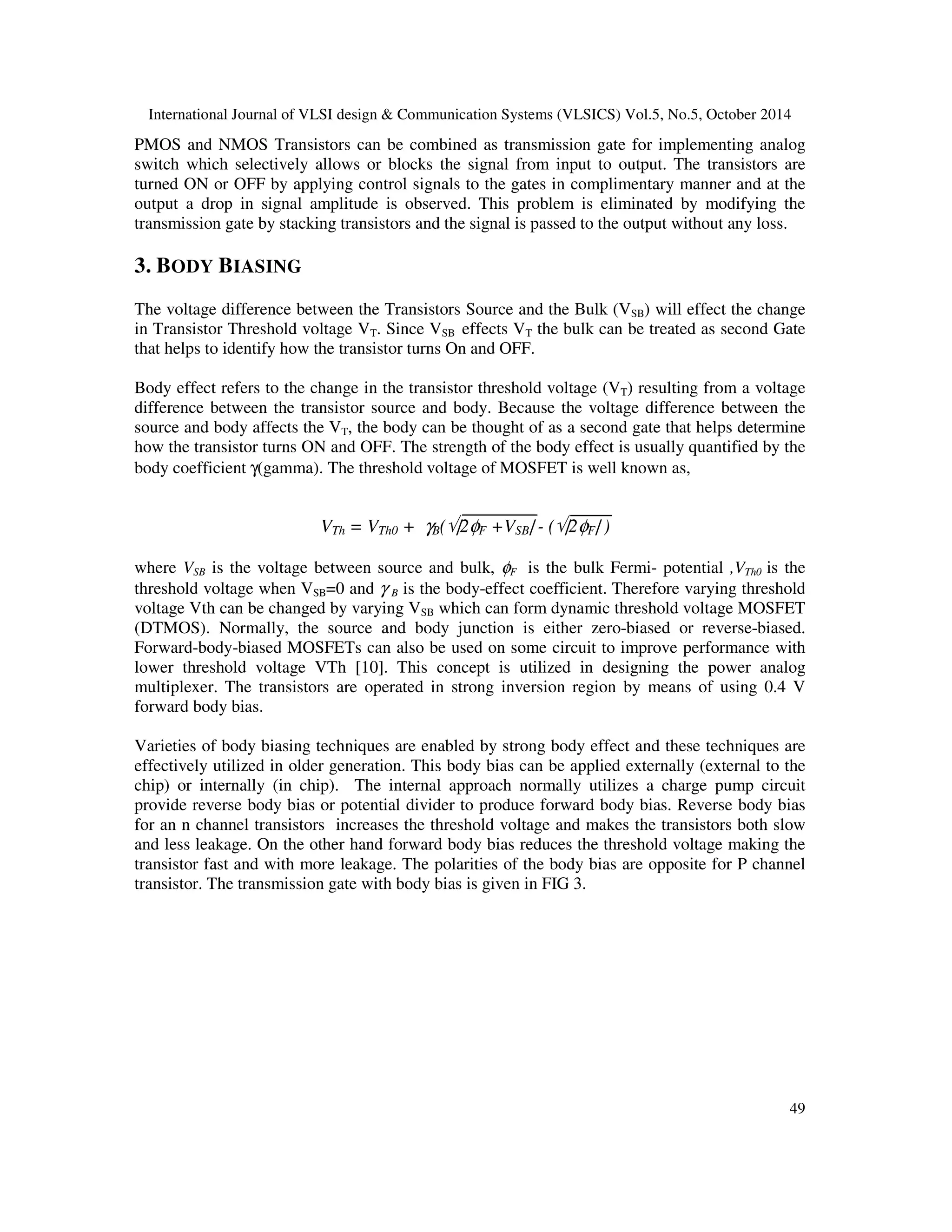
transistor. The transmission gate with body bias is given in FIG 3.
11. International Journal of VLSI design Communication Systems (VLSICS) Vol.5, No.5, October 2014
50
FIG 3: Transmission gate with dynamic body bias.
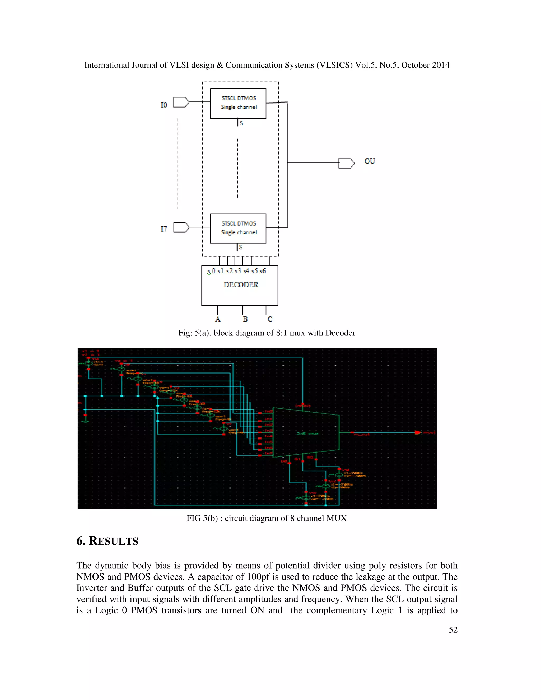
4. MULTIPLEXER DESIGN
Using the concept of a shift register large number of multiplexers designed in the past.
Synchronously triggered D-latches using external clock connected serially are used to build shift
register. Each D-latch enables one S H circuit. The clock feed-through to the output line is the
major disadvantage of this circuit. With each clock cycle glitches occur synchronously for every
positive and negative clock edge. The proposed multiplexer design minimizes this problem.
Instead of setting the body bias just once either during design or at production test, the Dynamic
body bias changes the body bias many times when the chip is operating. The temperature and
aging effects are minimized by Dynamic body bias and also the power management modes for
optimizing very low power operation are effectively utilized [7], [8].
A logic ‘1’ on SEL signal at the gate of NMOS transistors will turn them ON and a
complimentary SELBR connected to the gate of PMOS transistors will turn them ON and the
applied signal is allowed to pass from IN to OUT. On the other hand when the SEL is at logic’0’
and its complimentary SELBR will turn all the transistors OFF thereby blocking the signal from
IN to OUT. The output will be forced into a high-impedance state during the transition period
from ON to OFF where the junction capacitance will be charged to few millivolts.
A PMOS transistor connected as a pass transistor between the ground and the output node
minimizes this problem. Whenever all the transistors are in OFF state then the PMOS transistor
will be turned ON, forcing the output capacitor to discharge to ground.
The widths of the transistors are maintained in a ratio of 1:2 for NMOS to PMOS. The ON
resistance Ron of the switch is
1 1
Ron = =
gds μCox W (VGS – VTh)
L
12. International Journal of VLSI design Communication Systems (VLSICS) Vol.5, No.5, October 2014
The value of the ON-resistance depends on the overdrive voltage, Vov = Vgs – Vth and on the
aspect ratio, W/L through the trans conductance parameter μCox.
An analog loss less multiplexer with eight channels has been designed using this modified circuit
shown in FIG-3 for each channel. The channels are selected by three binary control inputs. The
inhibit input is used to Enable or Disable the multiplexer. A low ON resistance of 27 ohms, high
OFF resistance of 10Mohms,with very low leakage current in the order of Pico amperes were
obtained with the analog transmission gate.
51
5. STSCL GATES DECODER DESIGN
The logic gate designed using STSCL is AND gate and the schematic is given in the FIG 4
below. The circuit is simulated and analyzed so that nominal parameters of the STSCL can used
which will produce an optimum level output for the system.
FIG 4: Source coupled logic AND gate
This AND gate is modified into SCL Nand gate and a 3to 8 decoder is implemented using this
SCL nand gate. This is used to generate the select signals for each channel from three binary
control inputs. The block diagram and the circuit diagram of the system is shown in FIG 5(a)
(b).
13. International Journal of VLSI design Communication Systems (VLSICS) Vol.5, No.5, October 2014
52
Fig: 5(a). block diagram of 8:1 mux with Decoder
FIG 5(b) : circuit diagram of 8 channel MUX
6. RESULTS
The dynamic body bias is provided by means of potential divider using poly resistors for both
NMOS and PMOS devices. A capacitor of 100pf is used to reduce the leakage at the output. The
Inverter and Buffer outputs of the SCL gate drive the NMOS and PMOS devices. The circuit is
verified with input signals with different amplitudes and frequency. When the SCL output signal
is a Logic 0 PMOS transistors are turned ON and the complementary Logic 1 is applied to
14. International Journal of VLSI design Communication Systems (VLSICS) Vol.5, No.5, October 2014
NMOS transistors to turn ON which allows the signal to pass from IN to OUT. When the signal
goes to Logic 1, all transistors are turned OFF blocking the input signal. During the transition
period from ON to OFF the output will be forced into a high-impedance state where the junction
capacitance will be charged to few millivolts.
To avoid this drawback, a PMOS transistor is used between the output node and ground as a pass
transistor. When all the transistors are in OFF state, the PMOS transistor turns ON forcing the
output capacitor to discharge to ground. The system is simulated by applying sinusoidal input of
1μV amplitude and the frequency is varied from 1Hz onwards upto 1kHz.The total current drawn
by the circuit is around 1.98 μA resulting in the total power consumption of 0.79 μW. The
response of the system is shown in FIG’s 5(a),(b),(c). As the frequency of the input signal is
increased the power dissipation increased.
53
FIG 6(a): Simulated output with 1μV / 1KHz sinewave
FIG 6(b): Simulated output with 10μV / 1KHz sinewave
15. International Journal of VLSI design Communication Systems (VLSICS) Vol.5, No.5, October 2014
54
FIG 6(c): Simulated output with 10μV / 10KHz sinewave
The circuit is simulated by applying sinusoidal signals with an amplitude ranging from 1uV to
maximum of 0.4V to each channel. The channels are selected by changing the input control
signals of the decoder and the desired input is selected as shown in table-1
Table-1
INHIBIT INPUTS C B A OUTPUT
L X X X X L
H I0 L L L I0
H I1 L L H I1
H I2 L H L I2
H I3 L H H I3
H I4 H L L I4
H I5 H L H I5
H I6 H H L I6
H I7 H H H I7
The channel selection frequency is varied from DC to 10KHz. The output voltage is obtained
without any distortion and the simulated results are shown in the figures. 7(a), 7(b) and 7(c).
16. International Journal of VLSI design Communication Systems (VLSICS) Vol.5, No.5, October 2014
55
Fig: 7(a) simulated results with an amplitude of 1μV
Fig: 7(b)simulated results with an amplitude of 1mV
Fig: 7(c) simulated results with an amplitude of 100mV to 400mV
17. International Journal of VLSI design Communication Systems (VLSICS) Vol.5, No.5, October 2014
56
7. CONCLUSIONS
A low power wide range source coupled logic circuits operated in sub threshold region for
switching analog signals is implemented in 180nm technology using CADENCE TOOLS. The
required output voltage swing for proper logic operation is provided by using high resistance
PMOS load devices. Transmission gate circuit was used to switch analog signals with amplitude
ranging from 1μV onwards. The On and OFF resistance of the gate achieved was 27 ohms and
10M ohms respectively. The total power dissipated at a switching frequency of 10 KHz is around
0.79 μW. The STSCL circuit was used to implement 8 channel multiplexer for acquiring
biomedical signals and the power dissipated was measured as 0.79 μW. The number of channels
to be multiplexed can be increased further with suitable additional circuitry.
ACKNOWLEDGEMENTS
The authors are highly thankful to the Chairman of ANURAG GROUP OF INSTITUTIONS
Dr.P.Rajeshwar Reddy for his constant encouragement and also providing all the necessary
resources to carryout this work. They are also thankful to Dr. K.S.R.KRISHNA PRASAD,
Professor, NIT, Warangal for his valuable suggestions during this work.
REFERENCES
[1] M. Horowitz et al., “Low-power digital design,” in Proc. IEEE Int.Symp. Low Power Electronics and
Design (ISLPED), 1994, pp. 8–11.
[2] D. Suvakovic and C. A. T. Salama, “A low Vt CMOS implantation of an LPLV digital filter core for
portable audio applications,” IEEE Trans. Circuits Syst. II, Analog Digit. Signal process., vol. 47, no.
11,pp. 1297–1300, Nov. 2000.
[3] G. Gielen, “Ultra-low-power sensor networks in nanometer CMOS,” in Int. Symp. Signals, Circuits
and Systems (ISSCS), Jul. 2007, vol. 1,pp. 1–2.
[4] B. A.Warneke and K. S. J. Pister, “An ultra-low energy microcontroller for smart dust wireless sensor
networks,” in IEEE Int. Solid-State Circuits Conf. (ISSCC) Dig. Tech. Papers, 2004, pp. 316–317.
[5] L. S. Wong et al., “A very low-power CMOS mixed-signal IC for implantable pacemaker
applications,” IEEE J. Solid-State Circuits, vol.39, no. 12, pp. 2446–2456, Dec. 2004.
[6] C. Enz and E. Vittoz, Charge-Based MOS Transistor Modeling: TheEKV Model for Low-Power and
RF IC Design. New York: Wiley,2006.
[7] C. Enz, F. Krummenacher, and E. Vittoz, “An analytical MOS transistor model valid in all regions of
operation and dedicated to lowvoltage and low-current applications,” Analog Integr. Circuits Signal
Process. J., vol. 8, pp. 83–114, Jun. 1995.
[8] C. Enz, M. Punzenberger, and D. Python, “Low-voltage log-domain signal processing in CMOS and
BiCMOS,” IEEE Trans. Circuits Syst. II, Analog Digit. Signal Process., vol. 46, no. 3, pp. 279–289,
Mar.1999.
[9] B. H. Calhoun, A. Wang, and A. Chandrakasan, “Modeling and sizing for minimum energy operation
in subthreshold circuits,” IEEE J. Solid-State Circuits, vol. 40, no. 9, pp. 1778–1786, Sep. 2005.
[10] B. H. Calhoun and A. Chandrakasan, “Ultra-dynamic voltage scaling (UDVS) using subthreshold
operation and local voltage dithering,”IEEE J. Solid-State Circuits, vol. 41, no. 1, pp. 238–245, Jan.
2006.
[11] R. Amirtharajah and A. Chandrakasan, “A micropower programmable DSP using approximate signal
processing based on distributed arithmetic,”IEEE J. Solid-State Circuits, vol. 39, no. 2, pp. 337–347,
Feb.2004.
[12] H. Soeleman, K. Roy, and B. C. Paul, “Robust subthreshold logic for ultra-low-power operation,”
IEEE Trans. Very Large Scale Integr.(VLSI) Syst., vol. 9, no. 1, pp. 90–99, Sep. 2001.
18. International Journal of VLSI design Communication Systems (VLSICS) Vol.5, No.5, October 2014
[13] A. Chandrakasan and R. Brodersen, “Minimizing power consumption in digital CMOS circuits,”
57
Proc. IEEE, vol. 83, no. 4, pp. 498–523,Apr. 1995.
[14] A. Chandrakasan and R. Brodersen, “Minimizing power consumption in digital CMOS circuits,”
Proc. IEEE, vol. 83, no. 4, pp. 498–523,Apr. 1995.
[15] Hari Priya, Dr.K.S.Rao et al “Design of ultra low power 8-channel analog multiplexer using dynamic
threshold for biosignals” International Journal of VLSI design Communication Systems (VLSICS)
Vol.4, No.5, October 2013.
[16] Hari Priya, Dr.K.S.Rao et al “A low power front end analog multiplexing unit for 12 lead ecg signal
acquisition” International Journal of VLSI design Communication Systems (VLSICS) Vol.5, No.3,
June 2014.
[17] P.R.Gray, P. J.Hurst, S.H. Lewis, and R.G.Meyer, Analysis and Design of Analog Integrated
Circuits, Wiely, Fourth Ed., 2000
[18] C. C. Enz and E. A. Vittoz, Charge-based MOS Transistor Modeling, Wiley, 2006
AUTHORS
G.Deepika obtained her B.E., M.Tech degree in ECE in the year of 2002, 2005 from
CBIT, Osmania University and JNT University, Hyderabad respectively. She had 10 years
of teaching experience. Presently she is an Associate Professor in RRS College of
Engineering Technology, Medak District and pursuing Ph.D in JNT University,
Hyderabad.
P. Ramakrishna received his B. Tech, M. Tech degree in Electronics and Communication
Engineering (ECE), VLSI System Design in the years 2006, 2009 from NIT Warangal,
CVR College of Engineering JNT University Hyderabad respectively. He had 6 years of
teaching and research experience. Presently he is an Associate Professor Anurag Group of
Institutions (Autonomous) Hyderabad. His research interests include VLSI System
Design, Digital Signal Processing and Image processing.
Dr. K. S. Rao obtained his B. Tech, M. Tech and Ph.D. in Electronics and Instrumentation
Engineering in the years 1986, 89 and 97 from KITS, REC Warangal and VRCE Nagpur
respectively. He had 25 years of teaching and research experience and worked in all
academic positions, presently he is the Director, Anurag Group of Institutions
(Autonomous) Hyderabad. His fields of interests are Signal Processing, Neural Networks
and VLSI system design.