Download to read offline
![International Journal of VLSI design & Communication Systems (VLSICS) Vol.7, No.4, August 2016
DOI : 10.5121/vlsic.2016.7404 39
LEAKAGE REDUCTION TECHNIQUE AND
ANALYSIS OF CMOS D FLIP FLOP
Sridhara K and G S Biradar
Department of E & C E, P D A College of Engineering, Kalaburagi-585102
ABSTRACT
Power consumption and delay are the two major issues in the design of today‘s VLSI based battery
operated portable electronic devices. Memory units in these devices are made of flip flops and each flip
flop will consume more power in both active and idle conditions. Through this paper we try to explore
alternate techniques to implement D flip-flop with the aim of reducing leakage power, delay and to
increase the speed. All the different configurations of D flip-flops are simulated using HSPICE in 90nm
process technology with BSIM4 MOS transistor models of level 54.
KEYWORDS
Pass transistor, Transistor stacking, Leakage Power, LECTOR, VCLEARIT
1. INTRODUCTION
The expansion of battery operated portable device is continuously increasing the demand for low
power, minimum delay and high speed integrated circuits. In many of the portable devices the
standby periods are longer than the active periods and thus consume more power in the standby
state [2]. It is extremely important to reduce the power consumption in the standby mode. In
today’s high performance integrated circuits the leakage power contributes major power
consumption than overall total power consumption. In deep submicron circuits the leakage
power increases than the dynamic power and also in the circuits when there are no transitions at
the input and the transistors are in steady state [1]. Leakage power is mainly due to leakage
current that flows in the circuit when the circuit is operated in sleep or standby mode. The
leakage current is composed of sub-threshold leakage current, gate current, gate leakage current
and reverses biased leakage. Among all leakages, sub-threshold leakage contributes major part of
the leakage. The sub-threshold leakage current of a metal oxide semiconductor device is
expressed as
Where µo is the mobility of electrons/holes, Cox denotes oxide
capacitance of gate per unit area, W and L are width and channel length of MOS device
respectively, Vgs is the gate to source voltage Vt is the thermal voltage and η is the swing
coefficient. The contents of this paper are organized as follows: Section 2 describes some of the](https://image.slidesharecdn.com/7416vlsi04-160907053101/75/LEAKAGE-REDUCTION-TECHNIQUE-AND-ANALYSIS-OF-CMOS-D-FLIP-FLOP-1-2048.jpg)
![International Journal of VLSI design & Communication Systems (VLSICS) Vol.7, No.4, August 2016
40
work related to flip flops. Section 3 presents the design of D flips flop using MTCMOS
technique, pass transistor and pass transistor with transistor stacking. Section 4 presents two D
flip flop designs using LECTOR and VCLEARIT techniques. Section 5 gives the performance
comparison of the proposed flip flops. Section 6 draw the conclusion on the results obtained.
2. LITERATURE REVIEW
Flips flops are the basic memory and critical timing elements in digital systems. Flip flops
consumes more power both in active and idle mode and have large impact on speed and delay.
Researchers are continuously finding new techniques in the field of sequential circuits for
reduced power, delay and increased speed. In [5] author proposes a mixed and multi Vt flip flop
that reduces leakage power with slightly increased delay. In [6] author describes power gating
method of reducing the leakage power in a two phase complementary pass transistor adiabatic
logic. A clock skew scheduling algorithm to control leakage power is proposed in [7]. A
conventional data retention flip flop that uses a balloon latch applied to a transmission gate flip
flop is presented in [8]. A dual Vt method of reducing leakage power is enumerated in [9]. This
scheme assigns low threshold transistors to critical path and high threshold transistors to non
critical path to reduce leakage currents. D flip flop implementation using GDI technique is
proposed in [10]. In [16] author presents GDI multiplexer technique for the design of flip flop
and describes two architecture for it. Threshold voltage tuning methodology is proposed in [11]
to suppress the ground bouncing noise. A forward body bias generator is used to dynamically
tune the threshold voltage in different mode of operation of noise aware data preserving
sequential MTCMOS circuits. In [12] author presents a scheme for ultra low power system using
power gating to reduce leakage power dissipation in flip flops Sub clock power gating scheme is
proposed in [13] to minimize leakage power. During active mode leakage is controlled by clock
gating. In [14] self adjustable voltage level circuit is presented for controlling leakage power.
During active mode the self adjustable circuit supplies maximum voltage to the load and in the
silent mode lower voltage to the load. A clocked pair shared flip-flop (CPSFF) using Multi-
Threshold CMOS technique is presented in [17]. Double edge triggering and low swing clocking
is implemented in the clocking system. In [18] author presented a modified Single Edge
Triggered D flip flop design for various substrate bias voltages. In this design substrate of all
NMOS transistors are connected to supply and substrate of all PMOS transistors are connected to
ground.
3. CMOS D FLIP FLOP IMPLEMENTATION
D flip flop is widely used in the design of sequential circuits and memory storage devices.
Design of high speed and low power memory elements is desirable for the today’s battery
operated portable devices. Three different design of D flip flops are outlined in this section.
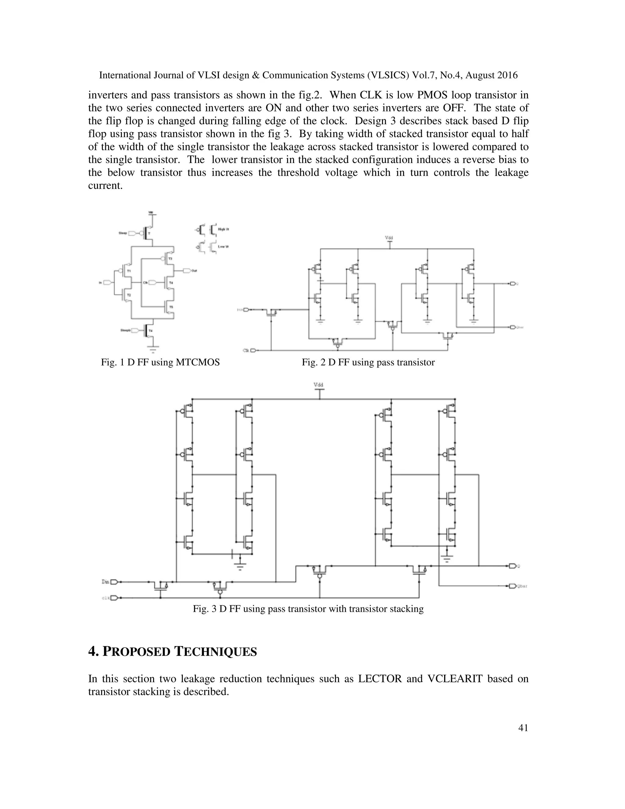
Design 1 uses MTCMOS technique that uses high Vt PMOS and NMOS devices to minimize
leakage current in the silent mode. The circuit is implemented by adding sleep transistors in the
pull up and pull down network of the 5T latch circuit is as shown in the fig. 1. When input and
CLK is high the transistors T1 and T5 are OFF and a transistor T2, T3 and T5 are ON and causes
the output to follow input. In this circuit high threshold transistors are used for sleep transistors.
In the active mode, the high Vt transistors are turned ON to keep the low Vt transistors to operate
with low switching power dissipation and minimum delay. In the idle mode high Vt transistors
are turned OFF to cut off the conduction path such that any leakage currents arise from internal
circuitry can be controlled. Design 2 uses master slave latch configuration to built flip flop using](https://image.slidesharecdn.com/7416vlsi04-160907053101/75/LEAKAGE-REDUCTION-TECHNIQUE-AND-ANALYSIS-OF-CMOS-D-FLIP-FLOP-2-2048.jpg)
![International Journal of VLSI design & Communication Systems (VLSICS) Vol.7, No.4, August 2016
42
4.1. STACK EFFECT
Stacking effect is known as turning OFF of more than one transistor in a stacked series connected
transistors to control leakage current. When two or more stacked transistors are turned OFF,
results in reduced DIBL effect. The model presented here is taken from leakage reduction model
in [3] and [4]. The leakage current Isub0 for a single turned-off transistor shown in fig. 4(a)
The leakage current of the stacked turned-off transistors shown in fig. 4(b) are
Assuming Wn0 = Wn1 = Wn also 1>>eVds0/Vt
the sub-threshold leakage current reduction factor
can be expressed as
Where Vx is the voltage between source of N0 to source of N1 can be obtained by solving
Isub0 = Isub1
Solving equations (9) and (10) to obtain leakage power reduction factor X. This factor is depends
only on the process parameter η and γ, hence leakage through stacked transistor is less than single
off transistor.](https://image.slidesharecdn.com/7416vlsi04-160907053101/75/LEAKAGE-REDUCTION-TECHNIQUE-AND-ANALYSIS-OF-CMOS-D-FLIP-FLOP-4-2048.jpg)
![International Journal of VLSI design & Communication Systems (VLSICS) Vol.7, No.4, August 2016
43
Fig. 4(a) Single transistor Fig. 4(b) Stacked transistor
4.2 LECTOR (LEAKAGE CONTROL TRANSISTOR) APPROACH
[15] In this approach D flip flop using pass transistor is modified by inserting self controlled
leakage control transistors (LCT’s) between pull up and pull down circuit as shown in the fig. 5.
One of the leakage transistors is always drives near the cut OFF for any input combination. The
gate of the LCT’s is controlled by the source of the other. These leakage control transistor
provides sufficient resistance between supply and ground during standby mode and hence
reduces the leakage current.
Fig. 5 D FF using LECTOR approach
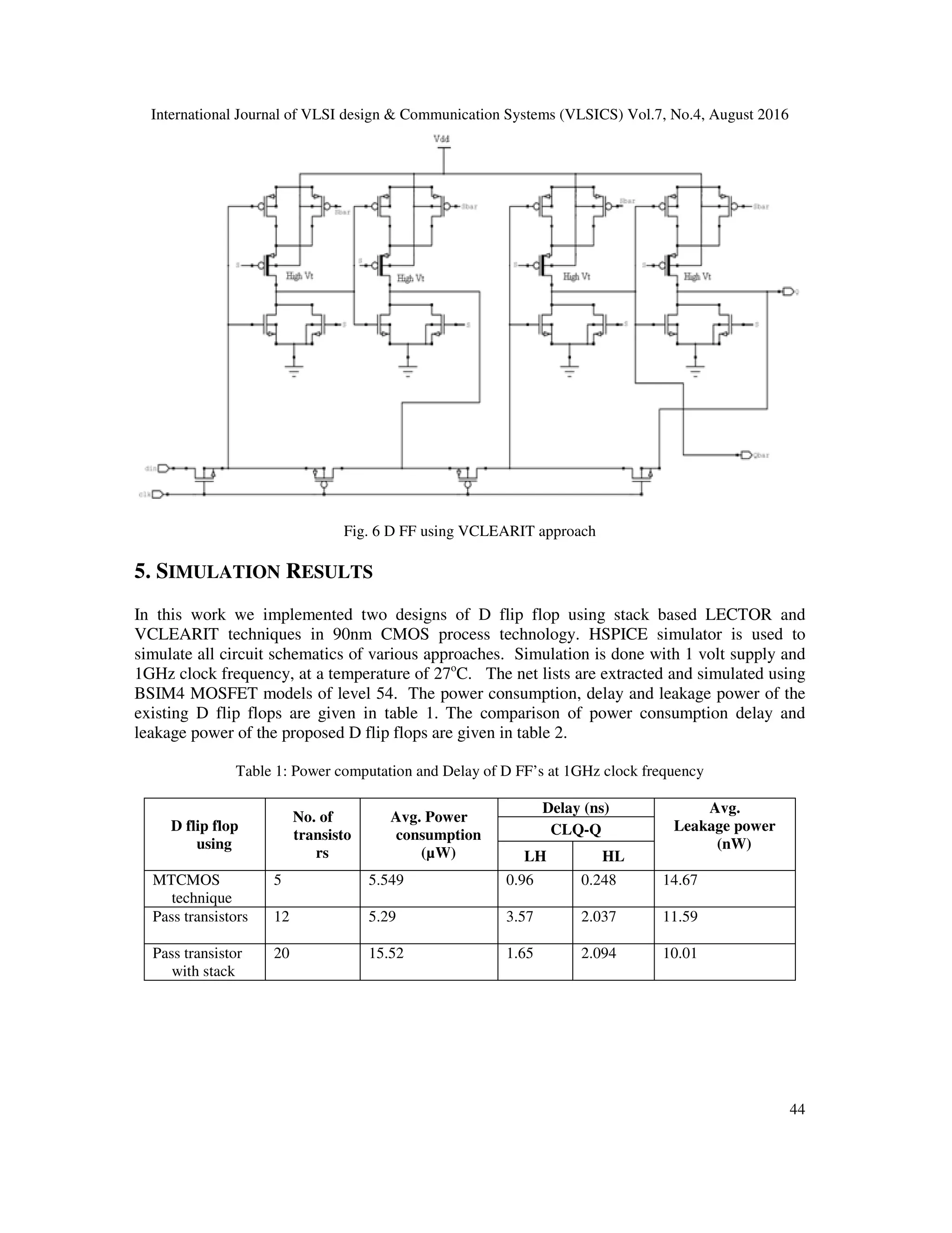
4.3 VCLEARIT (VLSI CMOS LEAKAGE REDUCTION) APPROACH
[16] In this approach a combination of high Vt and standard Vt to sleep transistors are connected
between pull up and pull down circuit of the D flip flop using pass transistor as shown in the fig.
6. During standby mode these sleep transistor are ON, providing a direct path from supply to
ground through high Vt transistor. Thus leakage loss is only through the high Vt transistor which
is turned OFF. In the active mode the sleep transistor are OFF to behave like CMOS logic.](https://image.slidesharecdn.com/7416vlsi04-160907053101/75/LEAKAGE-REDUCTION-TECHNIQUE-AND-ANALYSIS-OF-CMOS-D-FLIP-FLOP-5-2048.jpg)
![International Journal of VLSI design & Communication Systems (VLSICS) Vol.7, No.4, August 2016
45
Table 2: Power computation and Delay of proposed D FF’s at 1GHz clock frequency
D flip flop using
No. of
transistors
Avg. Power
consumption
(µW)
Delay (ns) Avg.
Leakage
power
(nW)
CLQ-Q
LH HL
LECTOR
approach
20 36 1.72 2.13 1.194
VCLEARIT
approach
24 16.91 1.78 2.19 0.869
5. CONCLUSIONS
In this work CMOS implementation of D flip flop using LECTOR approach and VCLEARIT
approach is presented. The average power consumption of all design is calculated at 1GHz clock
frequency. Also the delay and average leakage power of each of the design is estimated. From
the simulated results we can draw that the leakage power decreases when reduction techniques
are applied. The percentage of leakage power reduction is more in VCLEARIT approach with
slightly increase in the delay. LECTOR approach gives minimum leakage with minimum delay
but consumes more power. Overall VCLEARIT and LECTOR approach can be consider for the
design of CMOS D flip flop with lesser leakage power.
REFERENCES
[1] K.Roy, S. Mukhopadhya, H. Mahmoodi-meimand, “Leakage Current Mechanism and Leakage
Reduction techniques in Deep-Submicrometer CMOS circuits,” Proceedings of the IEEE, Vol. 91,
No. 2, February 2003.
[2] B.S. Deepaksubramanyan and Adrian N, “Analysis of Sub-threshold Leakage Reduction in MOS
Digital Circuits,” Proceedings of the 13th NASA VLSI Symposium, USA, June 5-6 2014.
[3] M.C. Johnson, D. Somasekhar and K. Roy, “Models and Algorithms for Bounds on Leakage in
CMOS circuits,” IEEE Transactions on Computer Aided Design on Integrated Circuits and Systems,
Vol. 18, No. 6, pp 714-725, June 1999.
[4] S. Narendra, V. De, S. Borkar, D.A. Antoniadis and A.P. Chandrakasan, “Full-chip Subthreshold
Leakage Power Prediction and Reduction Techniques for Sub-0.18um CMOS,” IEEE Journal of
Solid State Circuits, Vol. 39, No.2, pp. 501-510, February 2004.
[5] Jaehyun Kim, Chungki Oh and Youngsoo Shin, “Minimizing Leakage Power of Sequential Circuits
Through Mixed-Vt Flip flops And Multi-Vt Combinational Gates,” Journal ACM Transactions on
Design Automation of Electronic Systems, Vol. 15 Issue 1, December 2009.
[6] Weiqiang Zhang, Yu Zhang, Shi Xuhua and Jianping Hu, “Leakage Reduction of Power Gating
Sequential Circuits Based on Complementary Pass-Transistor Adiabatic Logic Circuits,” Innovative
Computing & Communication, International Conference on and Information Technology & Ocean
Engineering, pp. 282-285, 2010.](https://image.slidesharecdn.com/7416vlsi04-160907053101/75/LEAKAGE-REDUCTION-TECHNIQUE-AND-ANALYSIS-OF-CMOS-D-FLIP-FLOP-7-2048.jpg)
![International Journal of VLSI design & Communication Systems (VLSICS) Vol.7, No.4, August 2016
46
[7] Meng Tie, Haiying Dong, Tong Wang and Xu Cheng, “Dual-Vth leakage reduction with Fast Clock
Skew Scheduling Enhancement, Design, Automation and Test,” Europe Conference & Exhibition
(DATE), 2010.
[9] Hamid Mahmoodi-Meimand and K Roy, “Data Retention Flip-flops for Power-Down Applications,”
Proceedings of IEEE International Symposium on Circuits and Systems (ISCAS 2004), pp. 677-680.
[10] Linfeng Li and Jianping Hu, “A Transmission Gate Flip-flop Based on Dual Threshold CMOS
Techniques,” Proceedings of IEEE International Symposium on Circuits and Systems (ISCAS 2009),
pp. 539-542.
[10] A Morgenstein, A. Fish and I. Wgner, “A Efficient Implementation of D Flip-flop using the GDI
Technique,” ISCAS 2004, pp 673-676.
[11] Hailong Jiao and VolkanKursun, “Noise-aware data preserving sequential MTCMOS circuits with
dynamic Forward body bias,” Journal of Circuits, Systems and Computers, Vol. 20, No. 1, pp. 125-
145, February 2011.
[12] Jianping Hu, Xiaoying Yu and Jindan Chen, “New Low-Leakage Flip-flops with Power-Gating
Scheme for Ultra-low Power Systems,” Information Technology Journal, pp. 2161-2167, 2011.
[13] Jatin N Mistry, Bashir M, Al-Hashimi, David Flynnand and Stephen Hill, “Sub-Clock Power-Gating
Technique for Minimizing Leakage Power During Active Mode,” EDAA, 2011.
[14] M. Janaki Rani and S. Malarkann, “Leakage Power Reduction and Analysis of CMOS Sequential
Circuits,” International Journal of VLSI design and Communication Systems (VLSICS) Vol.3, No.1,
February 2012.
[15] H. Narender and R. Nagarajan, “LECTOR: A technique for leakage reduction in CMOS circuits”,
IEEE trans. on VLSI systems, vol. 12, no. 2, Feb. 2004.
[16] Preetham Lakshmikanthan And Adrian Nunez, “VCLEARIT: A VLSI CMOS Circuit Leakage
Reduction Technique for Nanoscale Technologies,” ACM Sigarch Computer Architecture News-
Special Issue: ALPS’07 Vol. 35, Issue 5, December 2007, pp. 10-16, December 2007.
[17] Paanshul Dobriyal, Karna Sharma, Manan Sethi, “A High Performance D flip fop Design with Low
Power Clocking System using MTCMOS Technique,” Advance Computing Conference (IACC),
2013 IEEE 3rd International, pp 1524-1528, 22-23 Feb 2013.
[18] K.G.Sharma, “Modified SET D-Flip Flop Design for Low- Power VLSI Applications,” TENCON
©2011 IEEE.
AUTHOR
Mr. Sridhara K received his B.E degree from Kuvempu University in the year 2001, Karnataka, India and
M.Tech degree in Electronics Design and Technology from IISc. Bangalore in the year 2010. He has 13
years of teaching experience. Currently he is doing his Research in the area of Low Power VLSI Design in
Visveswariya Technological University Belagavi. His research interests include Low power VLSI design,
advanced digital system design and embedded system design. He has published many papers in both
national and international conferences and journals.](https://image.slidesharecdn.com/7416vlsi04-160907053101/75/LEAKAGE-REDUCTION-TECHNIQUE-AND-ANALYSIS-OF-CMOS-D-FLIP-FLOP-8-2048.jpg)

The document discusses various techniques for reducing leakage power and delay in CMOS D flip-flops to enhance the efficiency of VLSI designs for battery-operated devices. It introduces methods like MTCMOS, lector, and vclearit, comparing their performance in terms of power consumption and delay. Simulation results indicate that the vclearit approach achieves greater leakage power reduction while maintaining slight increases in delay.