Downloaded 16 times
![International Journal of VLSI design & Communication Systems (VLSICS) Vol.5, No.3, June 2014
DOI : 10.5121/vlsic.2014.5305 47
IMPACT OF PARAMETER VARIATIONS AND
OPTIMIZATION ON DG-PNIN TUNNEL FET
Priya Jhalani and Manisha Pattanaik
ABV-Indian Institute of Information Technology and Management,
Gwalior, India
ABSTRACT
The downscaling of conventional MOSFETs has come to its fundamental limits. TFETs are very attractive
devices for low power applications because of their low off-current and potential for smaller sub threshold
slope. In this paper, the impact of various parameter variations on the performance of a DG-PNIN Tunnel
field effect transistor is investigated. In this work, variations in gate oxide material, source doping, channel
doping, drain doping, pocket doping and body thickness are studied and all these parameters are optimized
as performance boosters to give better current characteristics parameters. After optimization with all these
performance boosters, the device has shown improved performance with increased on-current and reduced
threshold voltage and the Ion/Ioff ratio is > 106
.
KEYWORDS
Tunnel Field Effect Transistor (TFET), Band to Band Tunneling (BTBT), DG-PIN TFET, DG-PNIN TFET,
Ion/Ioff Ratio
1. INTRODUCTION
Since the invention of transistor at Bell labs, the semiconductor industry has been witnessed a
record growth in terms of revenue and transistor count on a chip with the trend following the well
known Moore’s law [1]. With each generation of scaled technology, the transistor performance
has been improved. But, the aggressive scaling of MOSFET to meet various design constraints
like low power consumption, smaller area, higher speed etc. is approaching to its fundamental
limits [2-3]. To replace conventional MOSFET, new device structures are being investigated
which must be compatible to CMOS circuit architecture and technology. Due to their low sub
threshold swing (SS<60mv/dec), less susceptibility to short channel effects (SCEs), very low
leakage current, Tunnel Field Effect Transistor (TFET) has been considered as an alternative for
low power CMOS applications[4-12].
However the main disadvantage of TFET is, its low on-current. Therefore many TFET
performance enhancing solutions have been proposed to enhance on-current such as 1)
Modification of the TFET architecture (Like Hetero structures [13-15], Strained Silicon [16],
High-k gate dielectric [17-18]), 2) Use of small band gap materials at tunnel junction to reduce
the tunneling height [19-23]), 3) Use of a pocket at source channel tunnel junction to reduce the
tunneling width[24] etc. All these ideas are considered as performance boosters but, all of these
performance boosters are often applied independently. Therefore, in consideration to achieve
better current characteristics of TFET, as many as possible performance boosters should be
applied to the device.
Tunnel FETs are gated reverse biased PIN diodes, where the gate is used to modulate an effective
tunneling barrier height. The injection mechanism of Tunnel FETs is based on band to band
tunneling (BTBT). To switch the device on, the diode is reverse biased and a voltage is applied to](https://image.slidesharecdn.com/impactofparametervariationsandoptimizationondg-pnintunnelfet-140708061813-phpapp01/75/Impact-of-parameter-variations-and-optimization-on-dg-pnin-tunnel-fet-1-2048.jpg)
![International Journal of VLSI design & Communication Systems (VLSICS) Vol.5, No.3, June 2014
48
the gate. When device is off, there will be a large tunnel barrier between the bands. Hence, charge
carriers will not tunnel from valence band to conduction band and a very small off-current will
flow. When the device is on, the bands are pushed down towards each other and current flows.
In this work, a double gate PNIN Tunnel field effect transistor (DG-PNIN-TFET) device is
designed and the impact of various parameter variations (like gate oxide material, doping, and
body thickness variations) has been investigated. Now based on the variation analyses, the device
parameters are optimized in order to work as performance boosters. After that, all these
performance boosters are applied to the device to get superior current characteristics.
2. DEVICE STRUCTURE AND SIMULATION PARAMETERS
By increasing the doping level of some part of channel region near the source region, electric
field can be increased. This small region is known as pocket and the device is called pocket doped
TFET [24]. In this paper, an n-type pocket layer is used near the p+ heavily doped source region.
The intrinsic region is lightly doped and drain region is n+ heavily doped. This device can be also
termed as PNIN TFET device. Fig.1 shows the basic device structure of double gate PNIN (DG-
PNIN) TFET. In this paper, double gate structure will be used due to better gate control provided
by both gates.
Figure 1. DG-PNIN-TFET Device Structure
The fundamental device parameters used for the device simulations are listed in table 1. All
simulations are performed using SILVACO ATLAS with nonlocal BTBT model, Shockley Read
Hall (SRH) and Fermi Dirac models [25] at room temperature with Vgs=1V.
Table 1. Parameters used in the simulation of the TFET
No. Parameter Value
1 Gate Oxide Thickness (tox) 3nm
2 Silicon Body Thickness (tBody) 15nm
3 Gate Length (Lg) 60nm
4 Gate Work Function 4.0ev
5 Channel Doping (Nchannel) 1017
atoms/cm3
6 Source Doping (p+
) and Drain Doping (n+
) 1020
atoms/cm3
7 Pocket Doping (Npocket) 1019
atoms/cm3
8 Pocket Length (Lpocket) 10nm
9 Gate Source Overlap (Lov) 5nm
A comparison graph of Ids-Vgs characteristics of various TFET topologies like SG-PIN, SG-
PNIN, DG-PIN and DG-PNIN TFET is presented in Fig. 2 and from the graph it can be seen that](https://image.slidesharecdn.com/impactofparametervariationsandoptimizationondg-pnintunnelfet-140708061813-phpapp01/75/Impact-of-parameter-variations-and-optimization-on-dg-pnin-tunnel-fet-2-2048.jpg)


![International Journal of VLSI design & Communication Systems (VLSICS) Vol.5, No.3, June 2014
56
ACKNOWLEDGEMENTS
The authors would like to thank to VLSI Design Lab., ABV-Indian Institute of Information
Technology and management, Gwalior, for providing the computational resources.
REFERENCES
[1] G.E. Moore, “Cramming more components on to the integrated circuits”, Electronics, vol. 38, no. 8,
pp. 114-117, Apr. 1965.
[2] Seabaugh, Alan C.; Qin Zhang, “Low-Voltage Tunnel Transistors for Beyond CMOS Logic”,
Proceedings of the IEEE, vol.98, no.12, pp. 2095-2110, Dec. 2010.
[3] J. D. Meindehl, Q. Chen, J. A. Davis, “Limits of Silicon Nano electronics for Terascale
Integration”,Science, vol. 293, pp. 2044-2049, 2001.
[4] Pan, A.; Songtao Chen; Chi On Chui, “Electrostatic Modeling and Insights Regarding Multigate
Lateral Tunneling Transistors”, Electron Devices, IEEE Transactions on, vol.60, no.9, pp. 2712-2720,
Sept. 2013.
[5] E. Gnani, A. Gnudi, S. Reggiani, and G. Baccarani, “Drain-conductance optimization in nanowire
TFETs by means of a physics-based analytical model”, Solid-State Electron., vol. 84, pp. 96-102, Jun.
2013.
[6] A. Mallik, and A. Chattopadhyay, “The impact of fringing field on the device performance of a p-
channel tunnel field-effect transistor with a high-k gate dielectric”, IEEE Transactions on Electron
Devices, Vol. 59, No. 2, pp. 277-282, 2012.
[7] A. M. Ionescu, and H. Riel, “Tunnel field-effect transistors as energy-efficient electronic switches”,
Nature, Vol. 479, pp. 329-337, 2011.
[8] D. Leonelli, A. Vandooren, R. Rooyackers, S. De Gendt, M. M. Heyns, and G. Groeseneken, “Drive
current enhancement in p-tunnel FETs by optimization of the process conditions,” Solid-State
Electron., vol. 65, no.6, pp. 28-32, Nov. 2011.
[9] A. Chattopadhyay, and A. Mallik, “Impact of a spacer dielectric and a gate overlap/underlap on the
device performance of a tunnel field-effect transistor”, IEEE Transactions on Electron Devices, Vol.
58, No. 3, pp. 677-683, 2011.
[10] W. Lee, and W. Choi, “Influence of inversion layer on tunneling field-effect transistors”, IEEE
Electron Device Lett., Vol. 32, No. 9,pp. 1191-1193, 2011.
[11] W. Y. Choi, B.-G. Park, J. D. Lee, and T.-J. K. Liu, “Tunneling field-effect transistors (TFETs) with
sub threshold swing (SS) less than 60 mV/dec,” IEEE Electron Device Lett., vol. 28, no. 8, pp. 743–
745, Aug. 2007.
[12] Brinda Bhowmick, Srimanta Baishya,” An Analytical Model for Fringing Capacitance in Double gate
Hetero Tunnel FET and Analysis of effect of Traps and Oxide charges on Fringing Capacitance”, in
International Journal of VLSI design & Communication Systems (VLSICS), vol. 3, no.1, Feb. 2012.
[13] A. S. Verhulst, W. G. Vandenberghe, K. Maex, S. De Gendt, M. M. Heyns, and G. Groeseneken,”
Complementary silicon-based heterostructure tunnel-FETs with high tunnel rates,” IEEE Electron
Device Lett., vol. 29, no. 12, pp. 1398–1401, Dec. 2008.
[14] L. Wang, E. Yu, Y. Taur and P. Asbeck, “Design of tunneling fieldeffect transistors based on
staggered hetojunctions for ultralowpower applications,” IEEE Electron Device Lett., vol. 31, no. 5,
pp- 431-433, May 2010.
[15] O. M. Nayfeh, C. N. Chleirigh, J. Hennessy, L. Gomez, J. L. Hoyt and D. A. Antoniadis, “Design of
Tunneling Field-Effect Transisitors Using Strained-Silicon/Strained-Germanium Type-II Staggered
Heterojunctions,” IEEE Electron Device Lett., vol. 29, no. 9, pp- 1074-1077, Sept. 2008.
[16] K. Boucart, W. Riess, and A. M. Ionescu, “Lateral strain profile as key technology booster for all-
silicon Tunnel FETs,” IEEE Electron Device Lett.,vol.30,no. 6, pp. 656-658, Jun.2009.
[17] K. Boucart and A. M. Ionescu, “Double-gate tunnel FET with high-κ gate dielectric,” IEEE
Trans.Electron Devices, vol. 54, no. 7, pp. 1725–1733, Jul. 2007.
[18] M. Schlosser, K. K. Bhuwalka, M. Sauter, T. Zilbauer, T. Sulima, and I. Eisele, “Fringing-induced
drain current improvement in the tunnel fieldeffect transistor with high-κ gate dielectrics,” IEEE
Trans. Electron Devices, vol. 56, no. 1, pp. 100–108, Jan. 2009.
[19] Beneventi, G.B.; Gnani, E.; Gnudi, A.; Reggiani, S.; Baccarani, G., “Dual-Metal-Gate InAs Tunnel
FET With Enhanced Turn-On Steepness and High On-Current,” Electron Devices, IEEE Transactions
on, vol.61, no.3, pp. 776-784, March 2014.](https://image.slidesharecdn.com/impactofparametervariationsandoptimizationondg-pnintunnelfet-140708061813-phpapp01/75/Impact-of-parameter-variations-and-optimization-on-dg-pnin-tunnel-fet-10-2048.jpg)
![International Journal of VLSI design & Communication Systems (VLSICS) Vol.5, No.3, June 2014
57
[20] A. Dey, B. Borg, B. Ganjipour, M. Ek, K. Dick, E. Lind, P. Nilsson, C. Thelander, and L.
Wernersson, “High current density InAsSb/GaSb tunnel field effect transistors,” in Device Research
Conference (DRC), 70th Annual, pp. 205-206, 18-20 June 2012.
[21] Moselund, K. E.; Schmid, H.; Bessire, C.; Bjork, M.T.; Ghoneim, H.; Riel, H., “InAs-.Si Nanowire
Heterojunction Tunnel FETs,” Electron Device Letters, IEEE, vol.33, no.10, pp. 1453-1455, Oct.
2012.
[22] Guangle Zhou; Li, R.; Vasen, T.; Qi, M.; Chae, S.; Lu, Y.; Zhang, Q.; Zhu, H.; Kuo, J.-M.; Kosel, T.;
Wistey, M.; Fay, P.; Seabaugh, A.; Huili Xing, “Novel gate-recessed vertical InAs/GaSb TFETs with
record high ION of 180 µA/µAm at VDS = 0.5 V,” Electron Devices Meeting (IEDM), IEEE
International , pp.32.6.1-32.6.4, 10-13 Dec. 2012.
[23] Zhao, H.; Chen, Y.; Wang, Y.; Zhou, F.; Xue, F.; Lee, J., “InGaAs Tunneling Field-Effect-Transistors
With Atomic-Layer-Deposited Gate Oxides,” Electron Devices, IEEE Transactions on, vol.58, no.9,
pp. 2990-2995, Sept. 2011.
[24] Ritesh Jhaveri, Venkatagirish Nagavarapu,Jason C. S. Woo, “Effect of Pocket Doping and Annealing
Schemes on the source -Pocket Tunnel Field-Effect Transistor” in IEEE transaction on Electron
Device. Vol.58, no. 1,pp. 80-86, Jan 2011.
[25] Atlas User manual, Silvaco Int., Santa Clara CA, 2013.](https://image.slidesharecdn.com/impactofparametervariationsandoptimizationondg-pnintunnelfet-140708061813-phpapp01/75/Impact-of-parameter-variations-and-optimization-on-dg-pnin-tunnel-fet-11-2048.jpg)

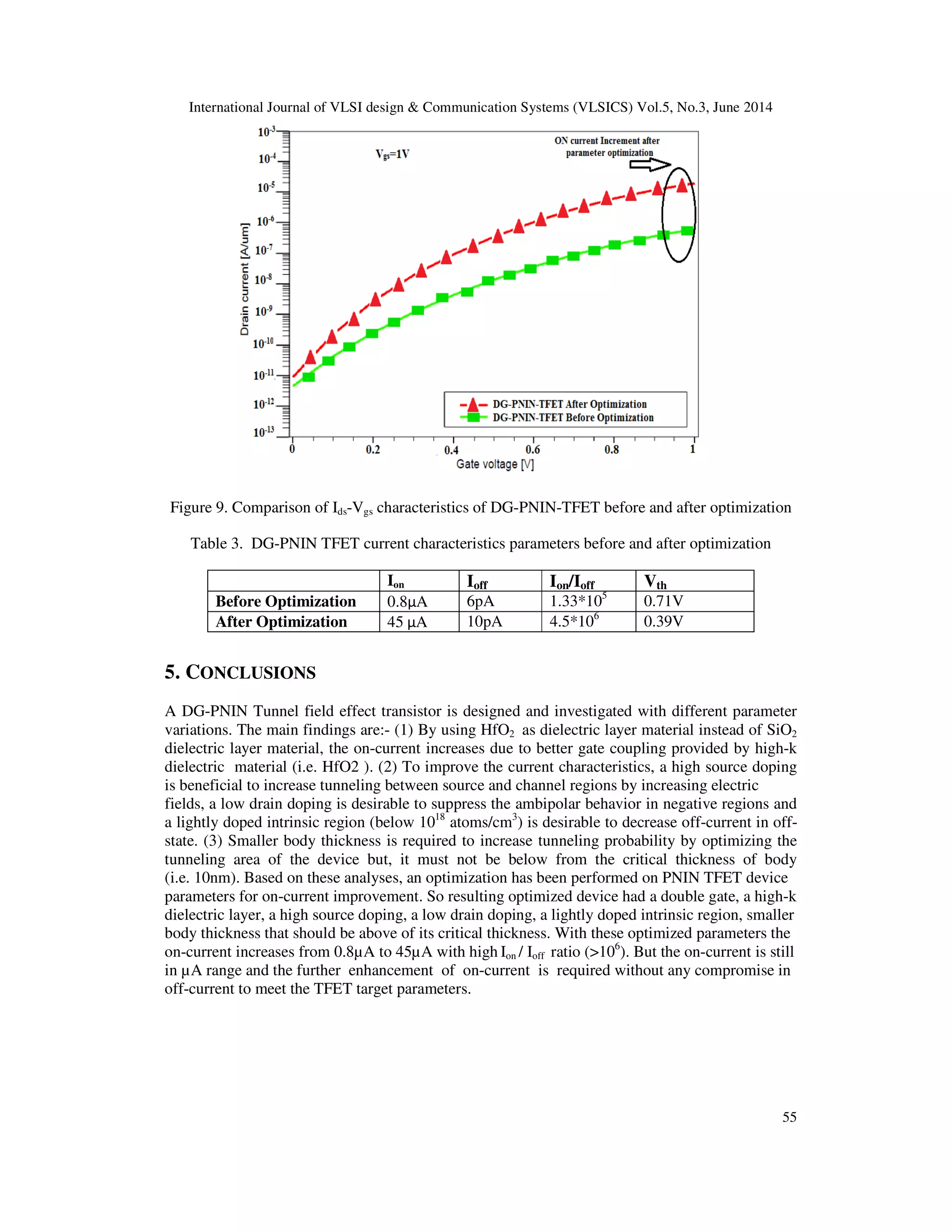
The paper investigates the optimization of the dg-pnin tunnel field-effect transistor (TFET) to enhance its performance for low-power applications. It evaluates the effects of various parameter variations, including gate oxide material, different doping levels, and body thickness on the device characteristics. After optimization, significant improvements were noted in on-current, threshold voltage, and the ion/ioff ratio exceeding 10^6, showcasing the advantages of applying multiple performance boosters collectively.


![Vibe Coding vs. Spec-Driven Development [Free Meetup]](https://cdn.slidesharecdn.com/ss_thumbnails/vibecodingvsspecdrivendevelopment-251209105622-43f455e7-thumbnail.jpg?width=640&height=640&fit=bounds)


