Downloaded 24 times
![2
Deptt.of Electronics and Communication Engineering
G. L. BAJAJ INSTITUTE OF TECHNOLOGY AND MANAGEMENT
[Approved by AICTE, Govt. of India & Affiliated to U.P.T.U, Lucknow]
CERTIFICATE
Certified that SUMIT KUMAR have carried out the lab project work presented
in this report entitled “REALIZATION OF 2:1 MUX USING TG” for the
award of Bachelor of Technology in Electronics and Communication
Engineering during the academic session 2015-16 from Uttar Pradesh
Technical University, Lucknow. The project embodies result of the work and
studies carried out by Student himself and the contents of the report do not form
the basis for the award of any other degree to the candidate or to anybody else.
(Mr. Dharmender Nishad) (Mr. DHARMENDRA NISHAD)
(Lab Co-ordinator) (Lab Co-ordinator)
(Asst. Professor) (Asst.Professor)
Deptt.of ECE Deptt.of ECE
H. O. D., Deptt.of ECE
Date:](https://image.slidesharecdn.com/areporton2to1muxusingtg-151205122825-lva1-app6892/75/A-report-on-2-to-1-mux-using-tg-2-2048.jpg)

![19
It is used for circuits with time–invariant sources (e.g. steady-state dc sources).
It calculates all nodal voltages and branch currents over a range of values. The
types of dc sweep analyses and their corresponding. (Dot) commands are
described below:
• Linear sweep: .DC [LIN] <sweep variable name> <start value> <end
value> <increment value>
• Logarithmic sweep: .DC <DEC|OCT> <sweep variable name> <start
value> <end value> <points value>
• Sweep over List of values: .DC <sweep variable name> LIST <value>*
All these sweep types can also be nested by adding another set of parameter
name and values at the end.
Transient Analysis
It is used for circuits with time variant sources (e.g., sinusoidal
sources/switched dc sources). It calculates all nodes voltages and branch
currents over a time interval and their instantaneous values are the outputs. The
corresponding. (Dot) command is as follows:
.TRAN <print step value> <final time value> [no-print value [step ceiling
value]] [SKIPBP]
AC Analysis
It is used for small signal analysis of circuits with sources of varying
frequencies. It calculates the magnitudes and phase angles of all nodal voltages
and branch currents over a range of frequencies. The corresponding. (dot)
command is as follows: .
AC <LIN|DEC|OCT> <Number of points> <Start frequency value> <End
frequency value>](https://image.slidesharecdn.com/areporton2to1muxusingtg-151205122825-lva1-app6892/75/A-report-on-2-to-1-mux-using-tg-19-2048.jpg)
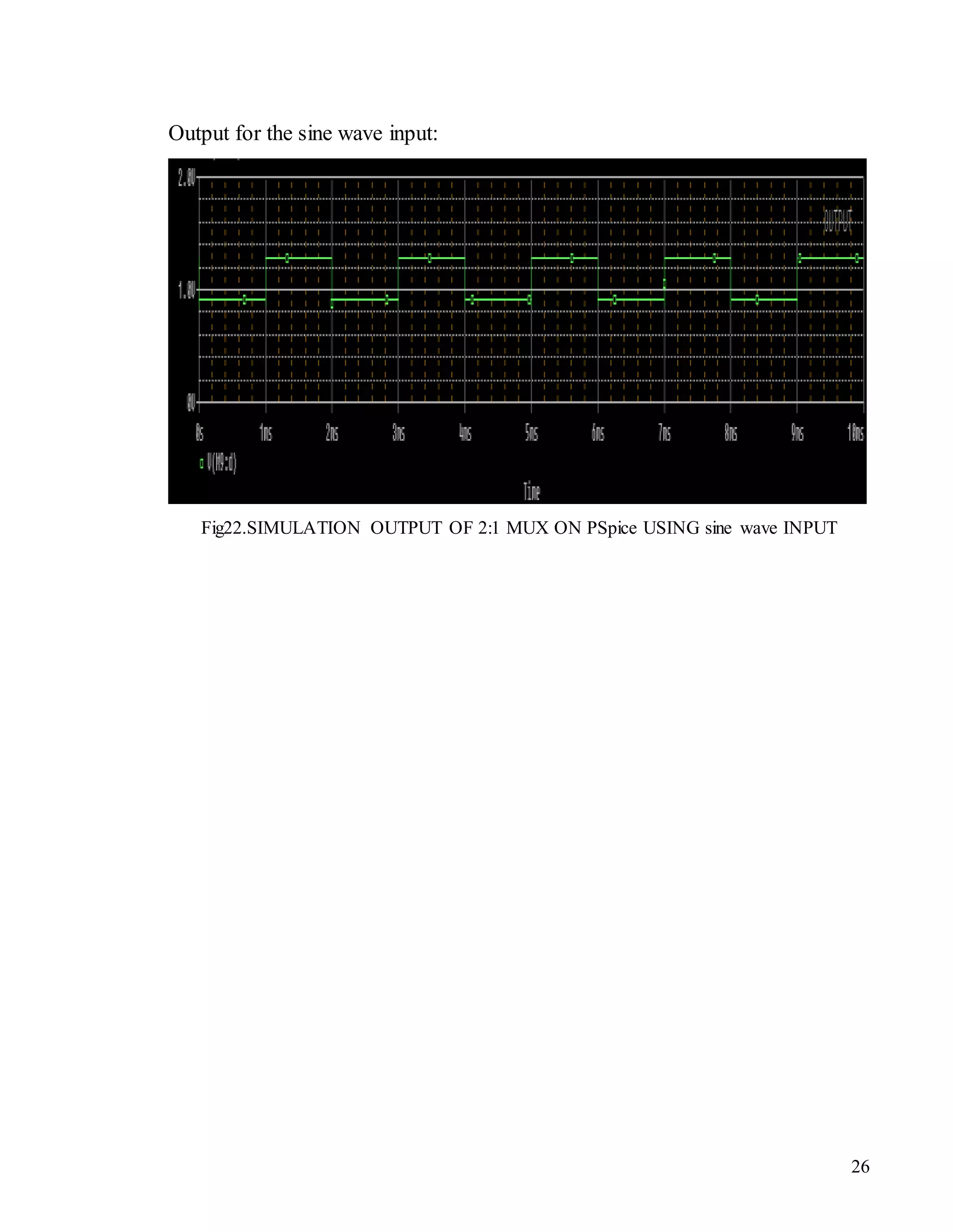

The document is a lab report by Sumit Kumar on the realization of a 2:1 multiplexer (MUX) using transmission gates as part of his Bachelor of Technology in Electronics and Communication Engineering at G. L. Bajaj Institute of Technology and Management. It details the project conducted during the 2015-16 academic session, highlighting the design, simulation using PSpice software, and behavior of the circuit. The report includes acknowledgments, abstracts, a comprehensive introduction, and concludes with references and findings.