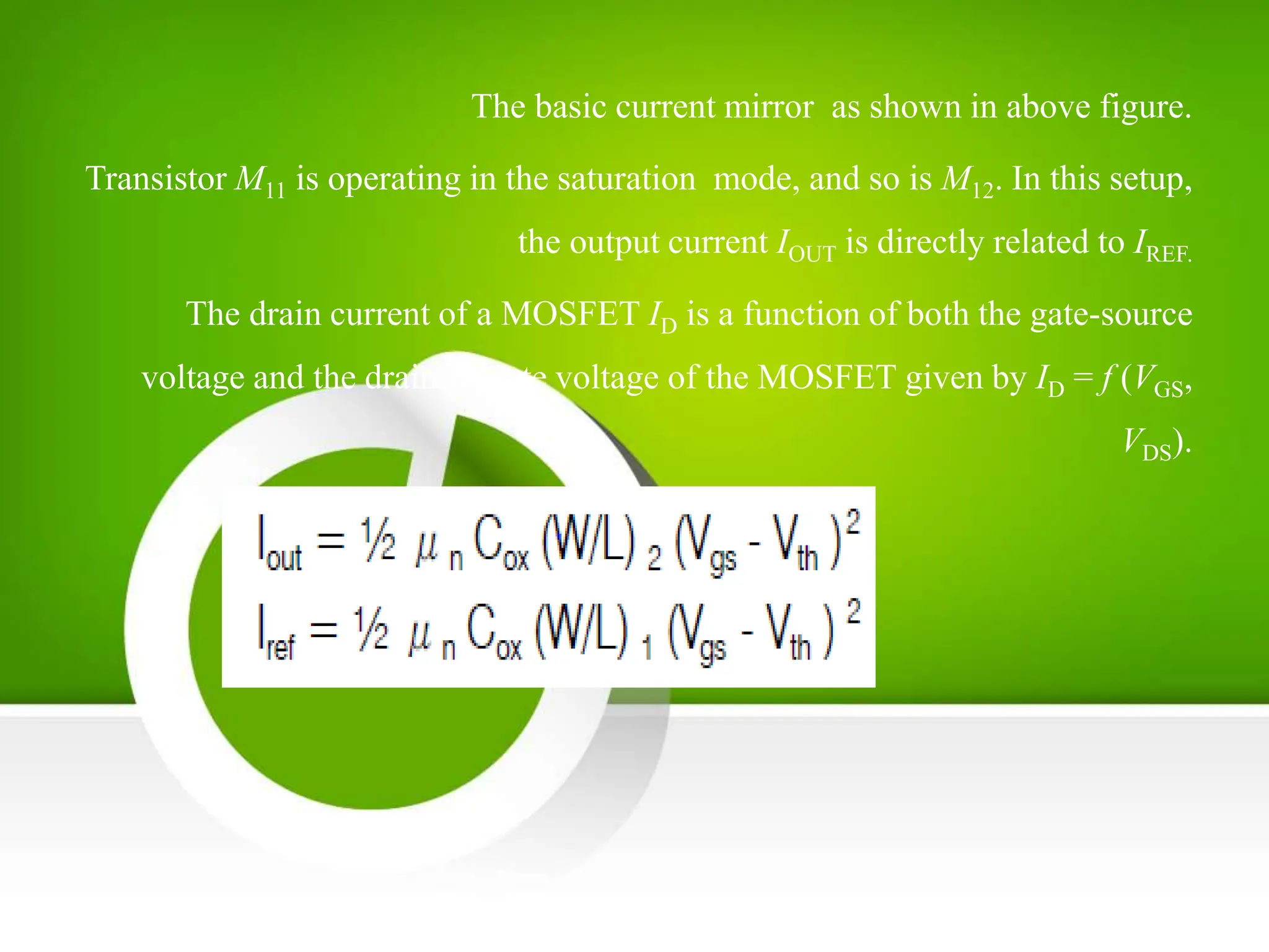
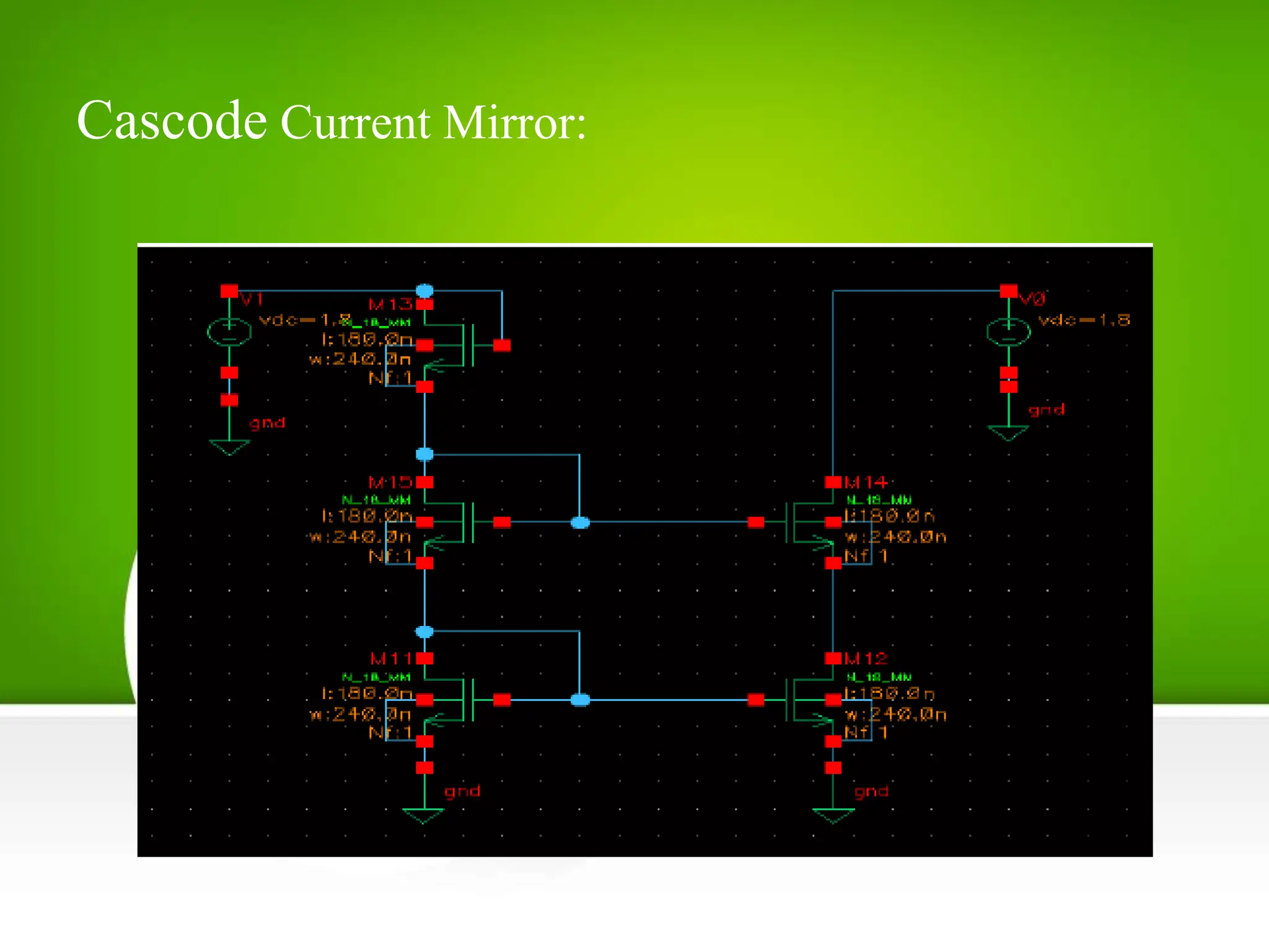
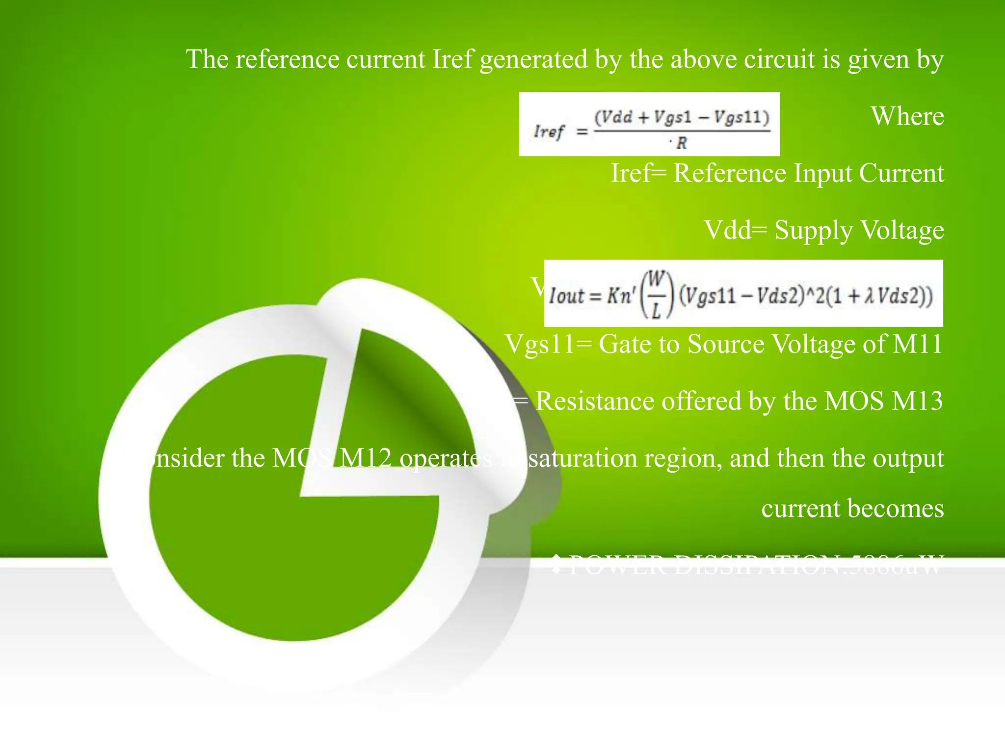
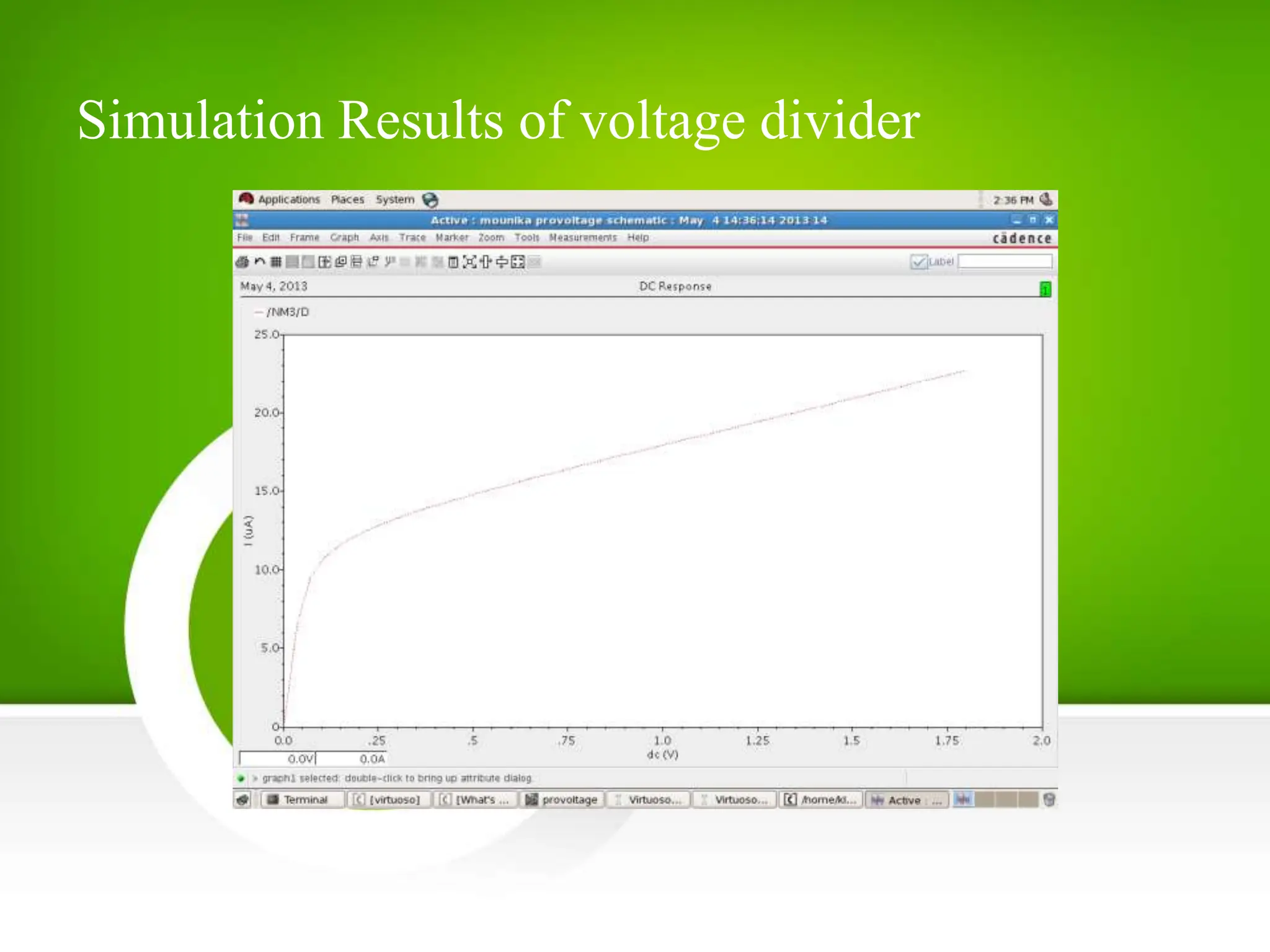
A New CMOS Voltage Divider Based Current
Mirror, Compared with the Basic and Cascode
Current Mirrors
Presented by
M.V.Mounika,
14204116.
Introduction:
Current Mirrors made by using active devices have come to be
widely used in analog integrated circuits both as biasing elements
and as load devices for amplifier stages.
The current mirror uses the principle that if the gate-source
potentials of two identical MOS transistors are equal, then the
current flown through their Drain terminals should be the same.
The use of current mirrors in biasing can result in superior
insensitivity of circuit performance to variations in power supply
and temperature.
NMOS current mirrors are used as current sinks and PMOS
current mirrors are used as current sources.
There is variety of Current Mirror circuits available, each of them
having their own advantage and applications
Current Mirror:
The basic current mirror as shown in above figure.
Transistor M11 is operating in the saturation mode, and so is M12. In this setup,
the output current IOUT is directly related to IREF.
The drain current of a MOSFET ID is a function of both the gate-source
voltage and the drain-to-gate voltage of the MOSFET given by ID = f (VGS,
VDS).
Limitations:
 Output resistance is finite and small value.
In basic current mirror circuit we can neglect the channel length
modulation.
POWER DISSIPATION: 116.39uW
Simulation Results of Basic Current Mirror
Cascode Current Mirror:
In order to suppress the effect of channel length modulation, a
cascade current source can be used.
The idea of cascode structure is employed to increase the output
resistance and the implementation requires NMOS technology.
Advantages:
High gain
High bandwidth
High slew rate
High stability and high input impedance
Limitations:
The minimum allowable voltage equal to two overdrive voltages
plus one threshold voltage.
Thus the cascade mirror wastes one threshold voltage in the
headroom.
This is the drawback of Cascode current mirror
POWER DISSIPATION:68.3217uW
Simulation Results of Cascode Current Mirror
CMOS Voltage Divider Current Mirror:
Figure shows the circuit of CMOS Voltage Divider based Current
Mirror.
Improved circuit uses NMOS and PMOS transistors to form a
Voltage Divider, so called as CMOS Voltage Divider based
current mirror.
NMOS and PMOS transistors are diode connected produces the
reference voltage Vgs to bias the NMOS transistor M12, which in
turns controls the Output Current Iout.
The reference current Iref generated by the above circuit is given by
Where
Iref= Reference Input Current
Vdd= Supply Voltage
Vgs1= Gate to Source Voltage of M1
Vgs11= Gate to Source Voltage of M11
R= Resistance offered by the MOS M13
Consider the MOS M12 operates in saturation region, and then the output
current becomes
POWER DISSIPATION:5886uW
Simulation Results of voltage divider
Applications:
High speed data converters such as RF, A/D, D/A converters
oscillators
CONCLUSION
• Main intention of this paper is to present the simple idea of designing a new
CMOS Voltage Divider based Current Mirror, than its comparison with the
Basic and Cascode Current Mirrors. This new Mirror is well suited for low
current biasing applications. Like the Wilson and Widler current Mirror
Circuits, this new Current Mirror can be used as a Low Current Biasing
circuit. Also, when compared with Basic Current Mirror, improved one
consumes only 1/4th of the Power consumed by the Basic Current Mirror.

mrvasbemounikaaaicd-150529174426-lva1-app6891.ppt

  • 1.
    A New CMOSVoltage Divider Based Current Mirror, Compared with the Basic and Cascode Current Mirrors Presented by M.V.Mounika, 14204116.
  • 2.
    Introduction: Current Mirrors madeby using active devices have come to be widely used in analog integrated circuits both as biasing elements and as load devices for amplifier stages. The current mirror uses the principle that if the gate-source potentials of two identical MOS transistors are equal, then the current flown through their Drain terminals should be the same.
  • 3.
    The use ofcurrent mirrors in biasing can result in superior insensitivity of circuit performance to variations in power supply and temperature. NMOS current mirrors are used as current sinks and PMOS current mirrors are used as current sources. There is variety of Current Mirror circuits available, each of them having their own advantage and applications
  • 4.
  • 5.
    The basic currentmirror as shown in above figure. Transistor M11 is operating in the saturation mode, and so is M12. In this setup, the output current IOUT is directly related to IREF. The drain current of a MOSFET ID is a function of both the gate-source voltage and the drain-to-gate voltage of the MOSFET given by ID = f (VGS, VDS).
  • 6.
    Limitations:  Output resistanceis finite and small value. In basic current mirror circuit we can neglect the channel length modulation. POWER DISSIPATION: 116.39uW
  • 7.
    Simulation Results ofBasic Current Mirror
  • 8.
  • 9.
    In order tosuppress the effect of channel length modulation, a cascade current source can be used.
  • 10.
    The idea ofcascode structure is employed to increase the output resistance and the implementation requires NMOS technology. Advantages: High gain High bandwidth High slew rate High stability and high input impedance
  • 11.
    Limitations: The minimum allowablevoltage equal to two overdrive voltages plus one threshold voltage. Thus the cascade mirror wastes one threshold voltage in the headroom. This is the drawback of Cascode current mirror POWER DISSIPATION:68.3217uW
  • 12.
    Simulation Results ofCascode Current Mirror
  • 13.
    CMOS Voltage DividerCurrent Mirror:
  • 14.
    Figure shows thecircuit of CMOS Voltage Divider based Current Mirror. Improved circuit uses NMOS and PMOS transistors to form a Voltage Divider, so called as CMOS Voltage Divider based current mirror. NMOS and PMOS transistors are diode connected produces the reference voltage Vgs to bias the NMOS transistor M12, which in turns controls the Output Current Iout.
  • 15.
    The reference currentIref generated by the above circuit is given by Where Iref= Reference Input Current Vdd= Supply Voltage Vgs1= Gate to Source Voltage of M1 Vgs11= Gate to Source Voltage of M11 R= Resistance offered by the MOS M13 Consider the MOS M12 operates in saturation region, and then the output current becomes POWER DISSIPATION:5886uW
  • 16.
    Simulation Results ofvoltage divider
  • 17.
    Applications: High speed dataconverters such as RF, A/D, D/A converters oscillators
  • 18.
    CONCLUSION • Main intentionof this paper is to present the simple idea of designing a new CMOS Voltage Divider based Current Mirror, than its comparison with the Basic and Cascode Current Mirrors. This new Mirror is well suited for low current biasing applications. Like the Wilson and Widler current Mirror Circuits, this new Current Mirror can be used as a Low Current Biasing circuit. Also, when compared with Basic Current Mirror, improved one consumes only 1/4th of the Power consumed by the Basic Current Mirror.