An analysis of pfc converter with high speed dynamic
•
1 like•358 views

This document analyzes the dynamic response of a power factor correction (PFC) converter. It discusses how the bandwidth of the compensator in the output voltage feedback loop affects the transient response. Specifically, it notes that a wider bandwidth improves response but introduces more voltage ripple, while a narrow bandwidth has slower response but less ripple. The document presents modeling of the converter with different levels of voltage ripple and analyzes how it impacts the static behavior and harmonic distortion. Simulation results demonstrate the tradeoff between response, ripple and power quality for low-bandwidth versus high-bandwidth designs.
![IJRET: International Journal of Research in Engineering and Technology eISSN: 2319-1163 | pISSN: 2321-7308
_______________________________________________________________________________________
Volume: 03 Special Issue: 12 | ICAESA - 2014 | Jun-2014, Available @ http://www.ijret.org 14
Fig 3: Expected waveforms in a PFC with appreciable
voltage ripple on control signal
The transient response of the output voltage loop will be
slow with this type of design. To achieve a faster transient
response, the bandwidth of the error amplifier AR, must be
relatively high, as a result leading to considerable voltage
ripple in the control signal, VA as shown in Figure. 2 Thus,
assuming that AR has been designed with high bandwidth
(allowing non-negligible voltage ripple on VA so as to
achieve a fast response), both the static and dynamic
behavior of the PFC change in relation to that corresponding
to a design with low-bandwidth in AR. The voltage ripple on
the control signal VA modifies both the static and dynamic
model of the power stage and has a strong effect on the line
current waveform obtained at the input of the PFC.
2. MODELING OF OUTPUT-VOLTAGE
FEEDBACK LOOP
The voltage and the current at the input of the power stage,
as shown in Fig. 1(b), can be written as follows:
vg(Lt) vgp sin(Lt) (1)
M
g L gp L A
K
I ( t) v sin( t) v (t)
(2)
Where vgp is the peak value of vg(ωLt), ωL is the line angular
frequency, KM is a constant and vA(t) is the voltage at the
error amplifier output. This voltage can be rewritten as
follows:
VA(t) vAdc vAac(t) (3)
VAac(t) VAacpsin(2Lt L) (4)
Where vAdc is the dc component of vA(t), vAac(t) is its ac
component, vAacp is the peak value of vAac(t) and φL is its
phase lag angle. The relative value of the voltage ripple on
vA(t) is defined as follows:
Adc
Aacp
V
k V
(5)
As there is a influence of voltage ripple on the control
signal, vA(t), all the static electrical quantities of the PFC
vary in relation to those corresponding to the standard design
case, i.e., with a control signal with no ripple. Figure 2 shows
some line waveforms corresponding to a variety of design
conditions. As this figure shows, the line current has
appreciable distortion, which is a consequence of the voltage
ripple on vA(t). It should be noted that only ripple of twice
the line frequency is assumed in vA(t), which is a logical
consequence of the behavior of both the RC output cell
(CBRL) and the error amplifier, AR, at frequencies greater
than twice the line frequency. Therefore, this voltage ripple
can be defined by means of only two parameters: its
magnitude, vAacp, and its phase lag angle, φL. As the voltage
ripple magnitude can be related to vAdc through k (5), then
vAdc, k and φL completely define the state of the control
variable, vA(t). Where these values have been expressed as
functions of k and φL and of the power stage variables (i.e.,
vgp, vo and RL). An important design parameter of any PFC is
the output voltage ripple. In the case of PFCs with a fast
output-voltage feedback loop, this ripple is mainly generated
by the current sources. The relative output voltage ripple of
twice the line frequency is compared with that of four times
the line frequency. Only in the case of high values of k (near
to 1) and φL≈ -90º does the value of line frequency become
significant.
The steady state expressions can be easily obtained as
Iop =
(2 sin )
2 0 1 2 2 sin
L L
L
R k
V k k
(6)
cos [( / )cos 2 ] 2 /2
1
L VAacp VAdc R L R L
(7)
The dc component of the output voltage is related to Iodc
through the impedance of the RLCB cell as:
Vodc = iodc [RL / (1+RLCBS)] (8)
3. SIMULATION RESULTS & DISCUSSION
The simulation model of the PFC boost converter is
maintained at 155V for both low bandwidth and high band
width. The output voltage has been boosted nearly 400V in
both cases. From figure 3 the gate pulses given for closed
loop PFC boost converter can be observed clearly and the
duty cycle of gate signal has been maintained constant
switching frequency (20 KHz).The major difference of low
bandwidth model from high bandwidth is considered with the
variation of the amplitude of the relative voltage ripple (k) on
the control signal and its phase lag angle ( L ) of the output
voltage controller. This can be observed from the following
figures clearly. Figure 3 Gate Pulses for closed loop system](data:image/gif;base64,R0lGODlhAQABAIAAAAAAAP///yH5BAEAAAAALAAAAAABAAEAAAIBRAA7)
Recommended
Recommended
More Related Content
What's hot
What's hot (20)
Viewers also liked
Viewers also liked (20)
Similar to An analysis of pfc converter with high speed dynamic
Similar to An analysis of pfc converter with high speed dynamic (20)
More from eSAT Publishing House
More from eSAT Publishing House (20)
An analysis of pfc converter with high speed dynamic
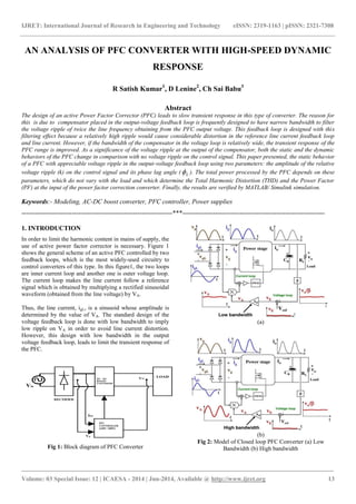
- 1. IJRET: International Journal of Research in Engineering and Technology eISSN: 2319-1163 | pISSN: 2321-7308 _______________________________________________________________________________________ Volume: 03 Special Issue: 12 | ICAESA - 2014 | Jun-2014, Available @ http://www.ijret.org 13 AN ANALYSIS OF PFC CONVERTER WITH HIGH-SPEED DYNAMIC RESPONSE R Satish Kumar1, D Lenine2, Ch Sai Babu3 Abstract The design of an active Power Factor Corrector (PFC) leads to slow transient response in this type of converter. The reason for this is due to compensator placed in the output-voltage feedback loop is frequently designed to have narrow bandwidth to filter the voltage ripple of twice the line frequency obtaining from the PFC output voltage. This feedback loop is designed with thi s filtering effect because a relatively high ripple would cause considerable distortion in the reference line current feedback loop and line current. However, if the bandwidth of the compensator in the voltage loop is relatively wide, the transient response of the PFC range is improved. As a significance of the voltage ripple at the output of the compensator, both the static and the dynamic behaviors of the PFC change in comparison with no voltage ripple on the control signal. This paper presented, the static behavior of a PFC with appreciable voltage ripple in the output-voltage feedback loop using two parameters: the amplitude of the relative voltage ripple (k) on the control signal and its phase lag angle ( L ). The total power processed by the PFC depends on these parameters, which do not vary with the load and which determine the Total Harmonic Distortion (THD) and the Power Factor (PF) at the input of the power factor correction converter. Finally, the results are verified by MATLAB/ Simulink simulation. Keywords:- Modeling, AC-DC boost converter, PFC controller, Power supplies ---------------------------------------------------------------------***----------------------------------------------------------------- 1. INTRODUCTION In order to limit the harmonic content in mains of supply, the use of active power factor corrector is necessary. Figure 1 shows the general scheme of an active PFC controlled by two feedback loops, which is the most widely-used circuitry to control converters of this type. In this figure1, the two loops are inner current loop and another one is outer voltage loop. The current loop makes the line current follow a reference signal which is obtained by multiplying a rectified sinusoidal waveform (obtained from the line voltage) by VA. Thus, the line current, igL, is a sinusoid whose amplitude is determined by the value of VA. The standard design of the voltage feedback loop is done with low bandwidth to imply low ripple on VA in order to avoid line current distortion. However, this design with low bandwidth in the output voltage feedback loop, leads to limit the transient response of the PFC. Fig 1: Block diagram of PFC Converter (a) (b) Fig 2: Model of Closed loop PFC Converter (a) Low Bandwidth (b) High bandwidth
- 2. IJRET: International Journal of Research in Engineering and Technology eISSN: 2319-1163 | pISSN: 2321-7308 _______________________________________________________________________________________ Volume: 03 Special Issue: 12 | ICAESA - 2014 | Jun-2014, Available @ http://www.ijret.org 14 Fig 3: Expected waveforms in a PFC with appreciable voltage ripple on control signal The transient response of the output voltage loop will be slow with this type of design. To achieve a faster transient response, the bandwidth of the error amplifier AR, must be relatively high, as a result leading to considerable voltage ripple in the control signal, VA as shown in Figure. 2 Thus, assuming that AR has been designed with high bandwidth (allowing non-negligible voltage ripple on VA so as to achieve a fast response), both the static and dynamic behavior of the PFC change in relation to that corresponding to a design with low-bandwidth in AR. The voltage ripple on the control signal VA modifies both the static and dynamic model of the power stage and has a strong effect on the line current waveform obtained at the input of the PFC. 2. MODELING OF OUTPUT-VOLTAGE FEEDBACK LOOP The voltage and the current at the input of the power stage, as shown in Fig. 1(b), can be written as follows: vg(Lt) vgp sin(Lt) (1) M g L gp L A K I ( t) v sin( t) v (t) (2) Where vgp is the peak value of vg(ωLt), ωL is the line angular frequency, KM is a constant and vA(t) is the voltage at the error amplifier output. This voltage can be rewritten as follows: VA(t) vAdc vAac(t) (3) VAac(t) VAacpsin(2Lt L) (4) Where vAdc is the dc component of vA(t), vAac(t) is its ac component, vAacp is the peak value of vAac(t) and φL is its phase lag angle. The relative value of the voltage ripple on vA(t) is defined as follows: Adc Aacp V k V (5) As there is a influence of voltage ripple on the control signal, vA(t), all the static electrical quantities of the PFC vary in relation to those corresponding to the standard design case, i.e., with a control signal with no ripple. Figure 2 shows some line waveforms corresponding to a variety of design conditions. As this figure shows, the line current has appreciable distortion, which is a consequence of the voltage ripple on vA(t). It should be noted that only ripple of twice the line frequency is assumed in vA(t), which is a logical consequence of the behavior of both the RC output cell (CBRL) and the error amplifier, AR, at frequencies greater than twice the line frequency. Therefore, this voltage ripple can be defined by means of only two parameters: its magnitude, vAacp, and its phase lag angle, φL. As the voltage ripple magnitude can be related to vAdc through k (5), then vAdc, k and φL completely define the state of the control variable, vA(t). Where these values have been expressed as functions of k and φL and of the power stage variables (i.e., vgp, vo and RL). An important design parameter of any PFC is the output voltage ripple. In the case of PFCs with a fast output-voltage feedback loop, this ripple is mainly generated by the current sources. The relative output voltage ripple of twice the line frequency is compared with that of four times the line frequency. Only in the case of high values of k (near to 1) and φL≈ -90º does the value of line frequency become significant. The steady state expressions can be easily obtained as Iop = (2 sin ) 2 0 1 2 2 sin L L L R k V k k (6) cos [( / )cos 2 ] 2 /2 1 L VAacp VAdc R L R L (7) The dc component of the output voltage is related to Iodc through the impedance of the RLCB cell as: Vodc = iodc [RL / (1+RLCBS)] (8) 3. SIMULATION RESULTS & DISCUSSION The simulation model of the PFC boost converter is maintained at 155V for both low bandwidth and high band width. The output voltage has been boosted nearly 400V in both cases. From figure 3 the gate pulses given for closed loop PFC boost converter can be observed clearly and the duty cycle of gate signal has been maintained constant switching frequency (20 KHz).The major difference of low bandwidth model from high bandwidth is considered with the variation of the amplitude of the relative voltage ripple (k) on the control signal and its phase lag angle ( L ) of the output voltage controller. This can be observed from the following figures clearly. Figure 3 Gate Pulses for closed loop system
- 3. IJRET: International Journal of Research in Engineering and Technology eISSN: 2319-1163 | pISSN: 2321-7308 _______________________________________________________________________________________ Volume: 03 Special Issue: 12 | ICAESA - 2014 | Jun-2014, Available @ http://www.ijret.org 15 Fig 4: Gate Pulses for closed loop system (a) (b) Fig 5: Response of line voltage & line current: (a) High bandwidth and (b) Low bandwidth (a) (b) Fig 6: Zoomed waveforms of Line voltage & Line current: (a) High bandwidth and (b) Low bandwidth
- 4. IJRET: International Journal of Research in Engineering and Technology eISSN: 2319-1163 | pISSN: 2321-7308 _______________________________________________________________________________________ Volume: 03 Special Issue: 12 | ICAESA - 2014 | Jun-2014, Available @ http://www.ijret.org 16 (a) (b) Fig 7: Input Current THD: (a) High bandwidth and (b) Low bandwidth (a) (b) Fig 8: Response of output voltage: (a) High bandwidth and (b) Low bandwidth It is clear from the the figure 4 (a) & (b) that the power factor has been improved in low band width than that of the high bandwidth. So the classical design of PFC is favorable with low bandwidth to get good power factor but the response is slow at the output side. Figure 5 (a) & (b) shows that the distortion of current response is more in the case of high bandwidth when compared with low bandwidthwidth. Figure 8 (a) & (b) shows the zoomed response of output voltage of boost converter in which the ripple can be observed. Though the ripple content in output voltage is less in case of low bandwidth, the response is slow. Though the ripple content in output voltage is considerable in case of high bandwidth, the response is fast. 4. CONCLUSIONS Table 1: Comparison of different factors of low bandwidth & high bandwidth PFCs Input Voltage (V) Input Power Factor Input Current THD (%) Voltage Ripple of V0 (V) Settling Time (Ts) (Sec) L H L H L H L H 90 0.916 0.927 7.69 5.65 15 60 0.358 0.06 125 0.914 0.917 5.46 5.38 35 48 0.160 0.090 150 0.916 0.921 6.90 6.83 38 47 0.221 0.131 H-High Bandwidth L-Low Bandwidth
- 5. IJRET: International Journal of Research in Engineering and Technology eISSN: 2319-1163 | pISSN: 2321-7308 _______________________________________________________________________________________ Volume: 03 Special Issue: 12 | ICAESA - 2014 | Jun-2014, Available @ http://www.ijret.org 17 The static behavior of a PFC with appreciable voltage ripple in the feedback loop 1has been observed in this model using two parameters: the amplitude of the relative voltage ripple (k) on the control signal and its phase lag angle ( L ). By the variation of these two parameters the required bandwidth to achieve fast transient response with appreciable voltage ripple can be obtained. ACKNOWLEDGEMENTS This work has been supported by the Research Promotion Scheme (AICTE-RPS) grant for the financial assistance provide under Ref.No: 8023/RID/RPS-54/Pvt (II Policy) / 2011-12. REFERENCES [1] M. J. Kocher and R. L. Steigerwald, "An ac-to-dc converter with high quality input waveforms", IEEE Trans. Ind. Appl., vol. 19, no. 4, 1983, pp.586-599. [2] L. H. Dixon, "High power factor preregulators for off-line power supplies", Unitrode Power Supply Design seminar, 1990, pp I2-1 to I2-16. [3] G. Spiazzi, P. Mattavelli, and L. Rossetto, “Methods to improve dynamic response of power-factor preregulators: an overview”, 6th European Conference on Power Electronics and Applications, 1995, pp. 3.754-3.759. [4] A. Fernández, J. Sebastián, P. J. Villegas, M. M. Hernando and D. G. Lamar, “Dynamic Limits of a Power-Factor Preregulator”, IEEE Trans. On Ind. Electron. vol. 52, no. 1, February 2005, pp.77-86. [5] J. Sebastián, D. G. Lamar, A. Fernández and M. M. Hernando, “Steady state analysis of power factor correctors with a fast output-voltage feedback loop”, IEEE APEC 09. [6] R. B. Ridley, “Average small-signal analysis of the boost power factor corrector circuit”, VPEC Seminar Proceedings 1989, pp. 108-120. [7] J. Sebasti´an, D. G. Lamar, M. M. Hernando, M. Rodr´ıguez, and A. Fern´andez, “Average small-signal modelling of the power stage of power factor correctors with a fast output-voltage feedback loop,” in Proc. IEEE Appl. Power Electron. Conf. Expo., 2009, pp. 998–1004. [8] J. Sebastian, D. G. Lamar, A. Rodrfguez, M.Arias and A. Fernandez., “On the maximum bandwidth attainable by power factor correctors with a standard compensator,” in Proc. IEEE Appl. Power Elctron.Conf.Expo..2009,pp.1872-1878. [9] J. Sebasti´an,A. Fern´andez, P.Villegas, M. M. Hernando, and J.M. Lopera,“A new active input current shaper for converters with symmetrically driven transformer,” IEEE Trans. Ind. Appl., vol. 37, no. 2, pp. 592–600, Mar./Apr. 2001. BIOGRAPHIES R. Satish Kumar was born in Kurnool, Andhra Pradesh, India in 1985. He received the B.Tech (Electrical and Electronics Engineering) degree from JNT University, Hyderabad affiliated college in 2007. He completed M.Tech (Power Electronics) in RGMCET (Autonomous), Nandyal, affiliated to JNTU Anantapur in 2013. He has Published/Presented technical research papers in international Journals/ Conferences. His field of interest includes AC-DC Converter, Power factor correction, Digital control Techniques. e-mail:satishraguru@gmail.com. D.Lenine was born in Pondicherry, India in 1978. He received the B.Tech (Electrical and Electronics Engineering) degree from Pondicherry University, India in 2004 and the M.Tech (Electrical Drives and Control) from same University in 2006 and Ph.D in Digital Controller based Power Factor Correction Converter from JNT University, Kakinada in 2013. In 2006 (October) he joined the Dept. Electrical and Electronics Engineering , R.G.M. College of Engineering and Technology, Nandyal, as a Assistant Professor. Currently he is working as an Associate Professor in Dept. of EEE. RGMCET, Nandyal. He has published/presented several technical research papers in national and international Journals/conferences. His field of interest includes AC-DC Converter, Power factor correction, Electrical Drives, Digital control Techniques, Digital control of electrical machines and Estimation of machines parameters. e-mail:lenine_2004@yahoo.com. Ch. Sai Babu received the B.E from Andhra University (Electrical & Electronics Engineering), M.Tech in Electrical Machines and Industrial Drives from REC, Warangal and Ph.D in Reliability Studies of HVDC Converters from JNTU, Hyderabad. Currently he is working as a Professor in Dept. of EEE in JNTUCE, Kakinada. He has published several National and International Journals and Conferences. His area of interest is Power Electronics and Drives, Power System Reliability, HVDC Converter Reliability, Optimization of Electrical Systems and Real Time Energy Management. e-mail: chs_eee@yahoo.co.in.