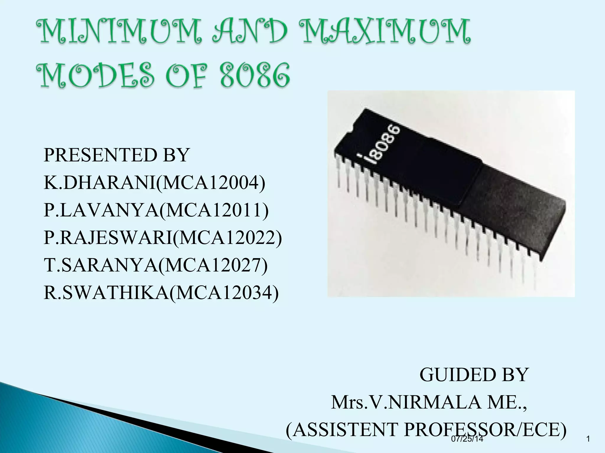
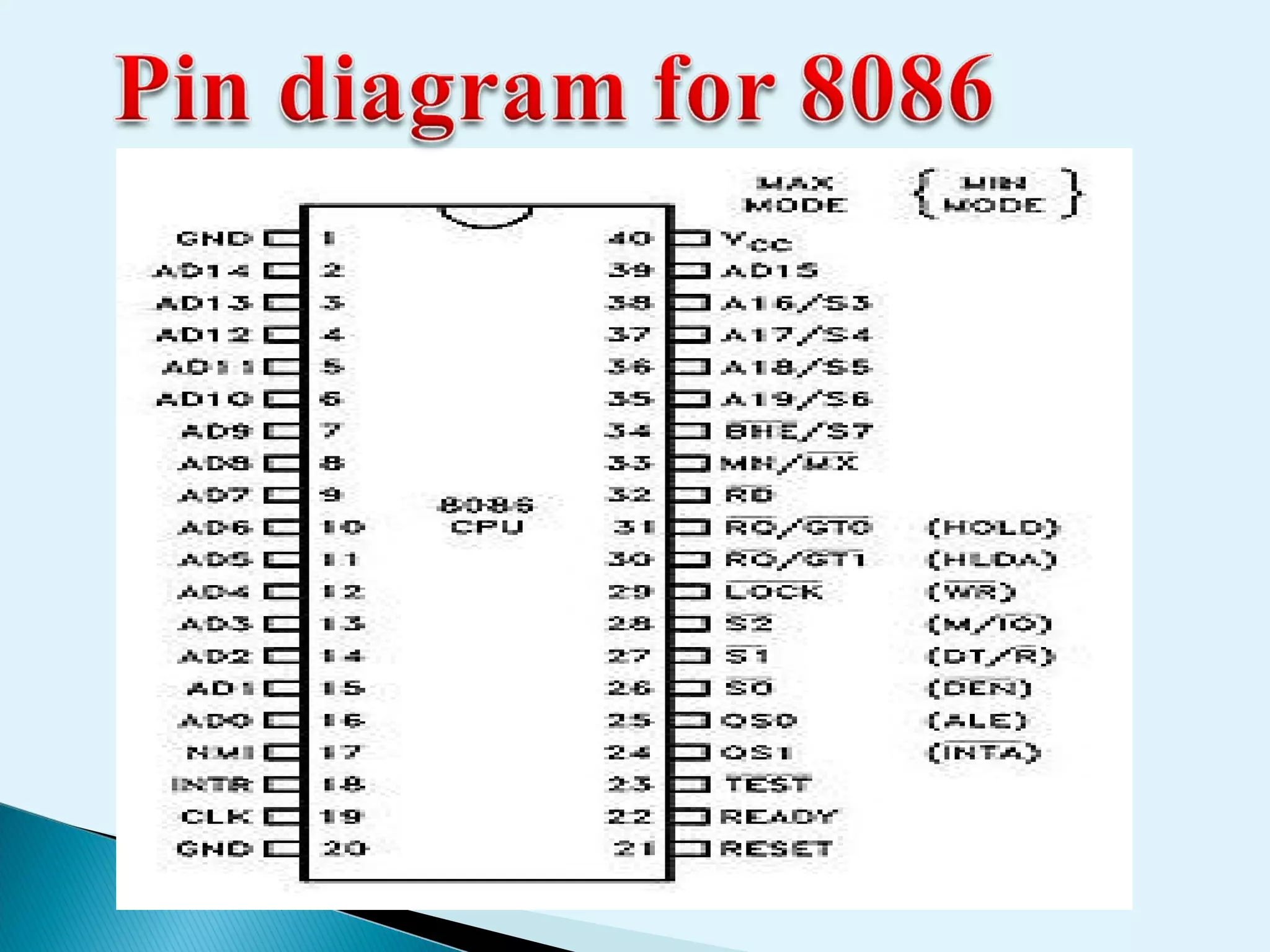
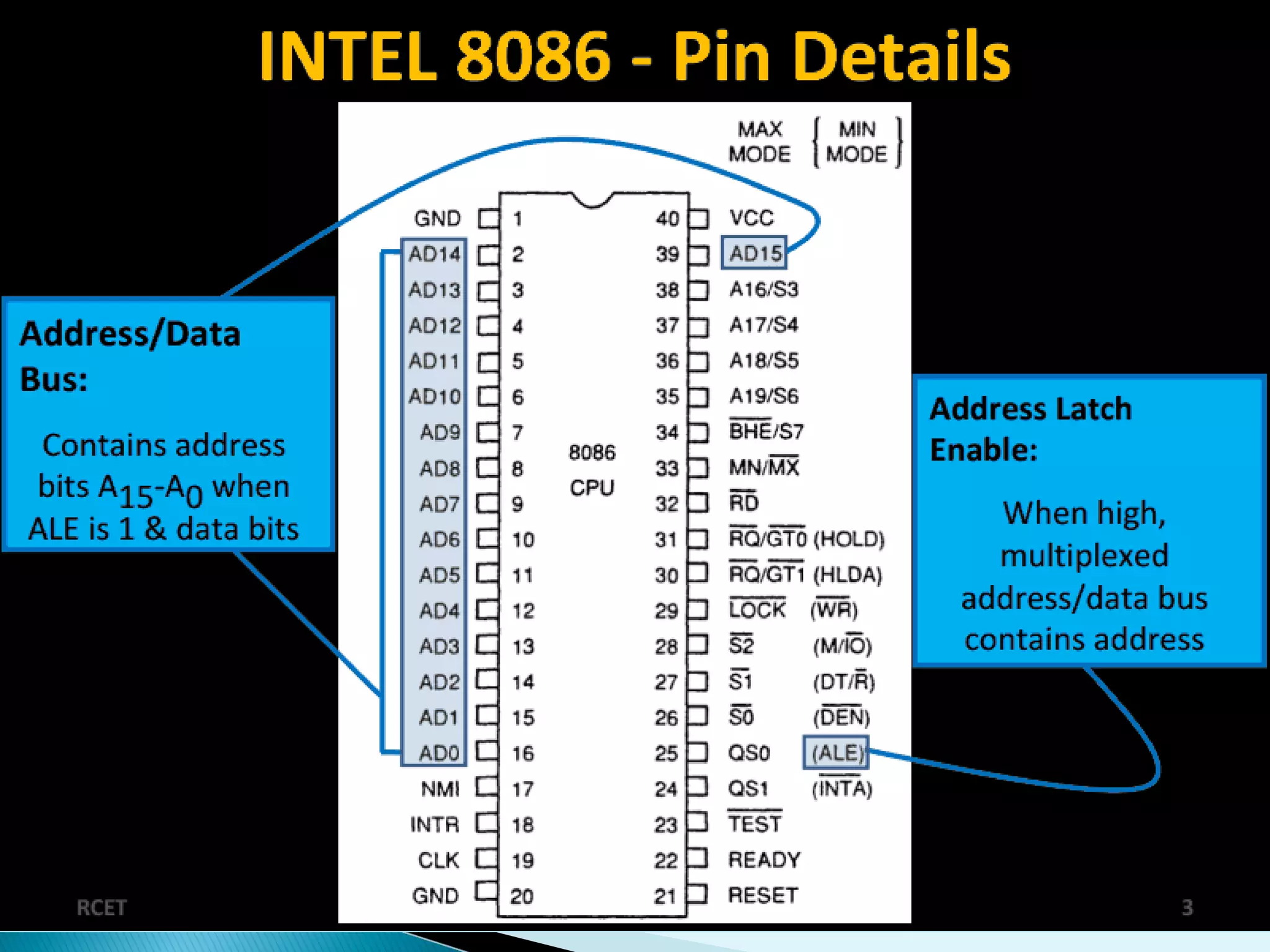
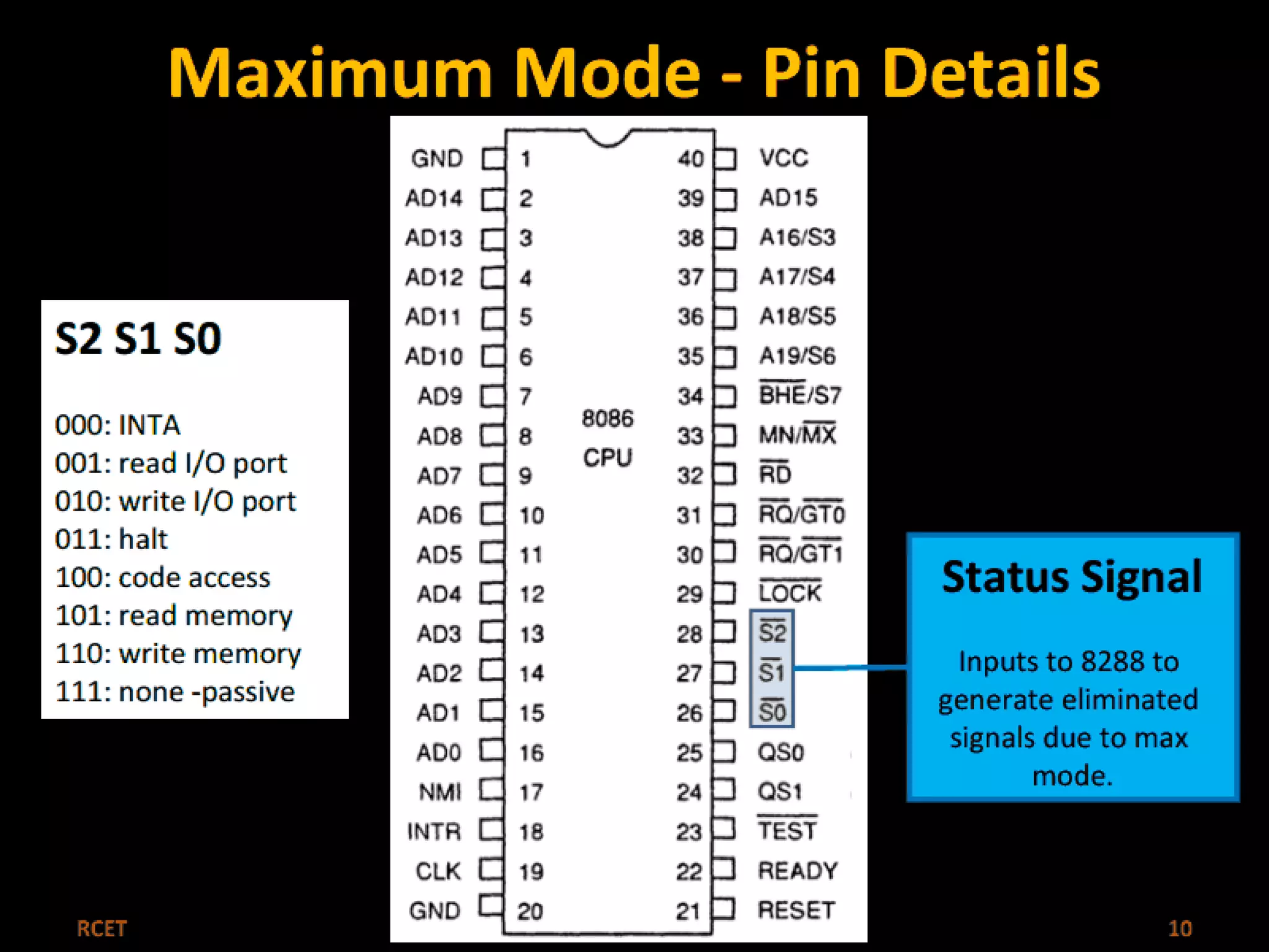
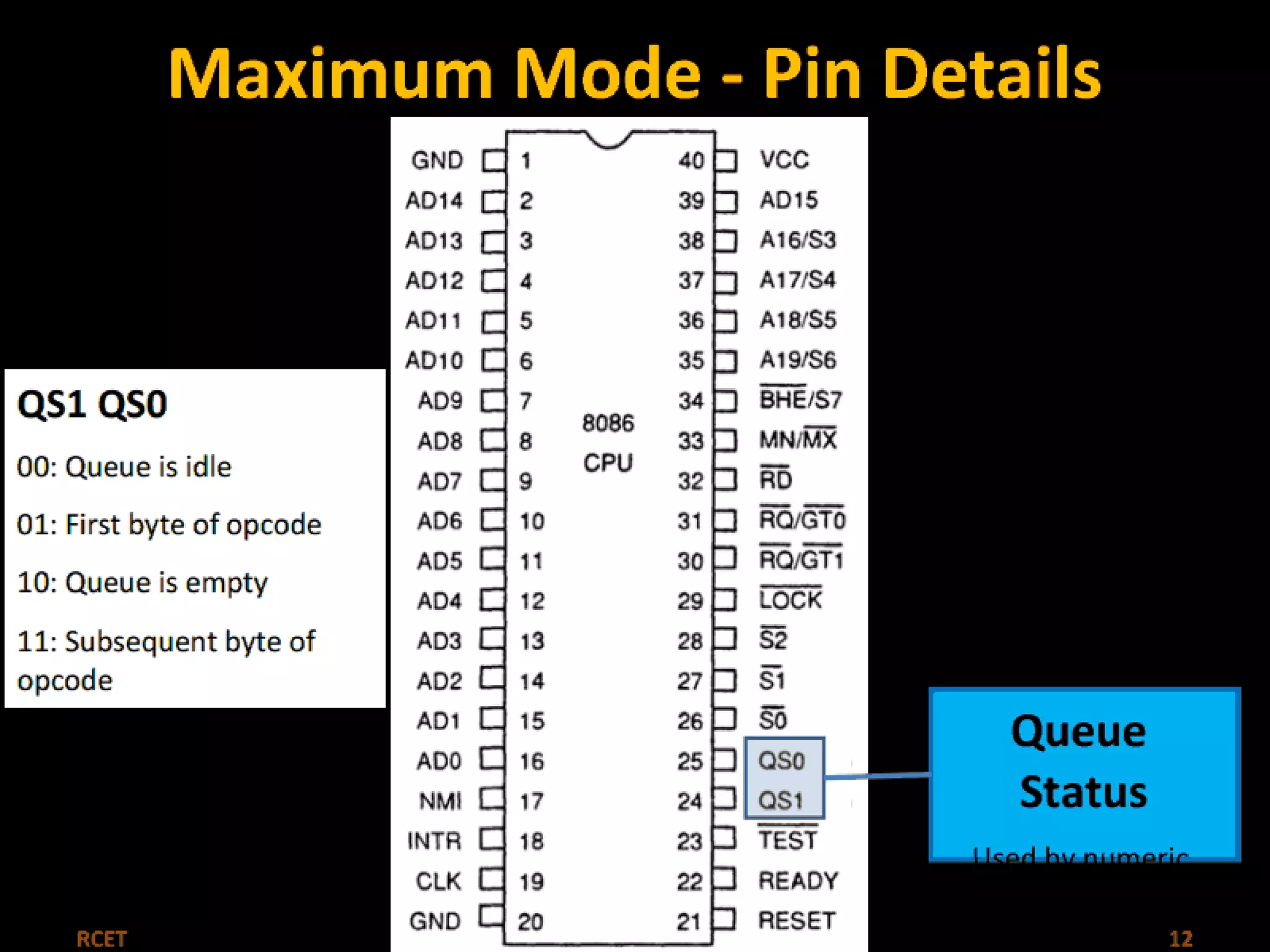
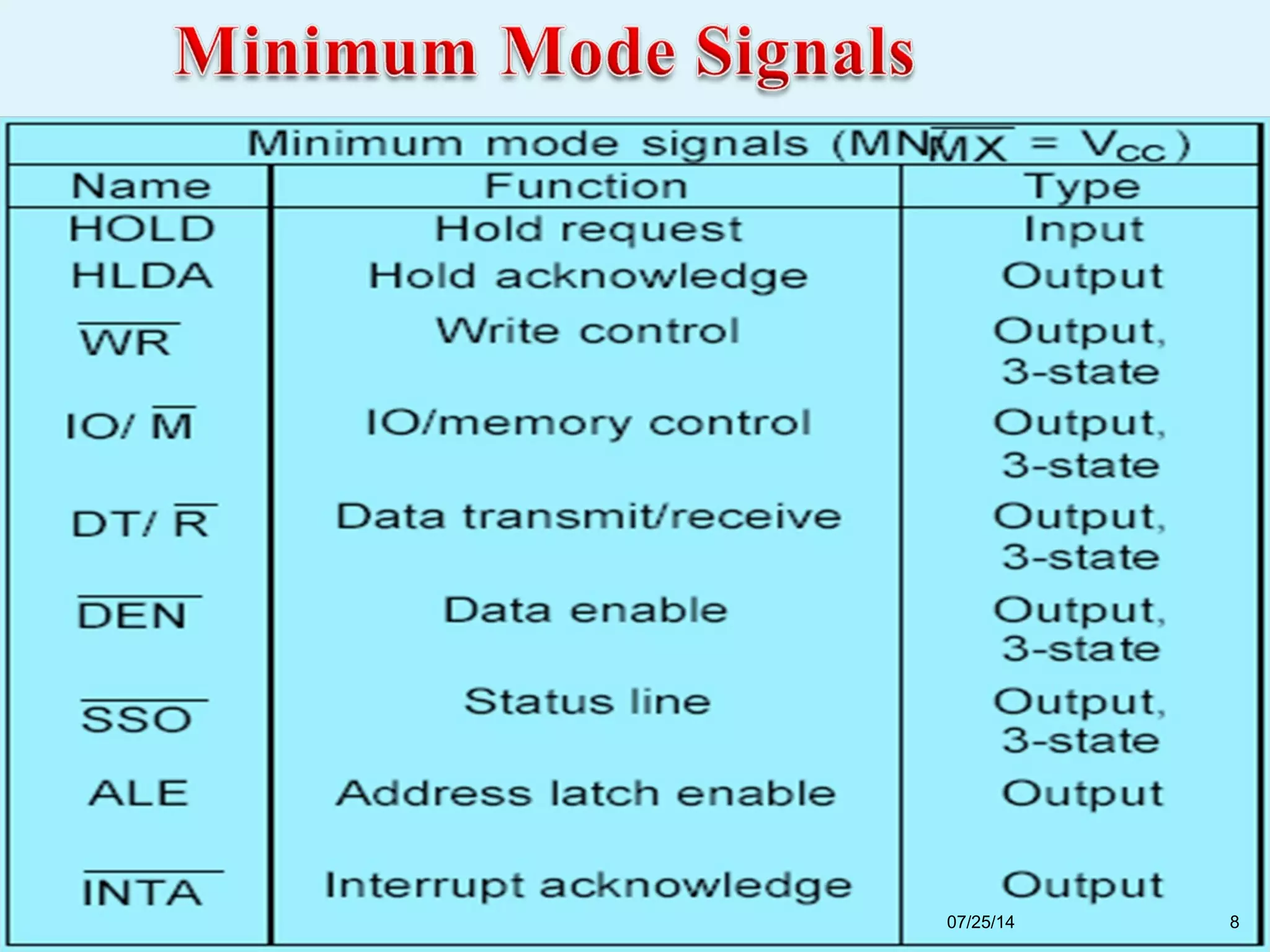
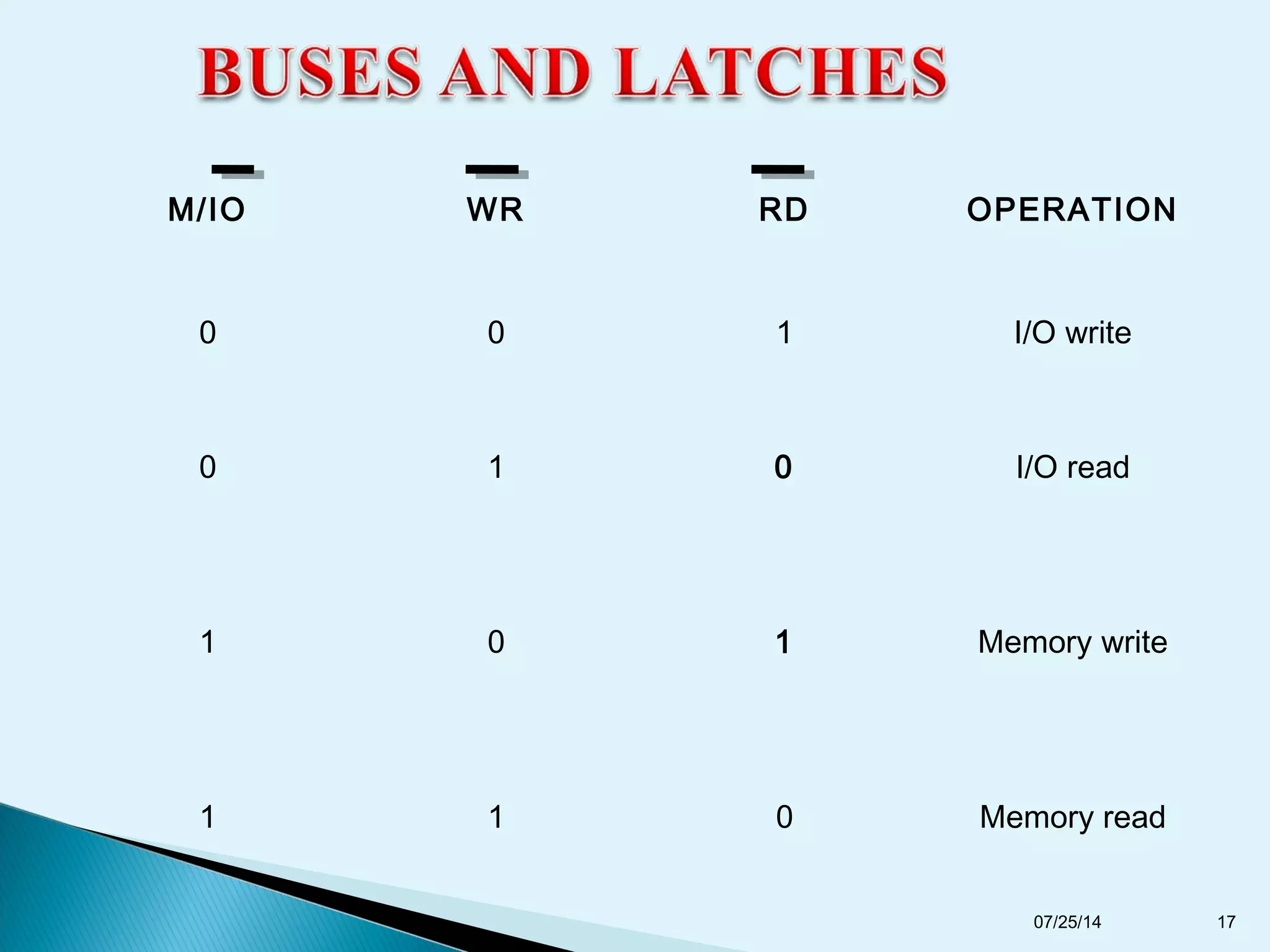
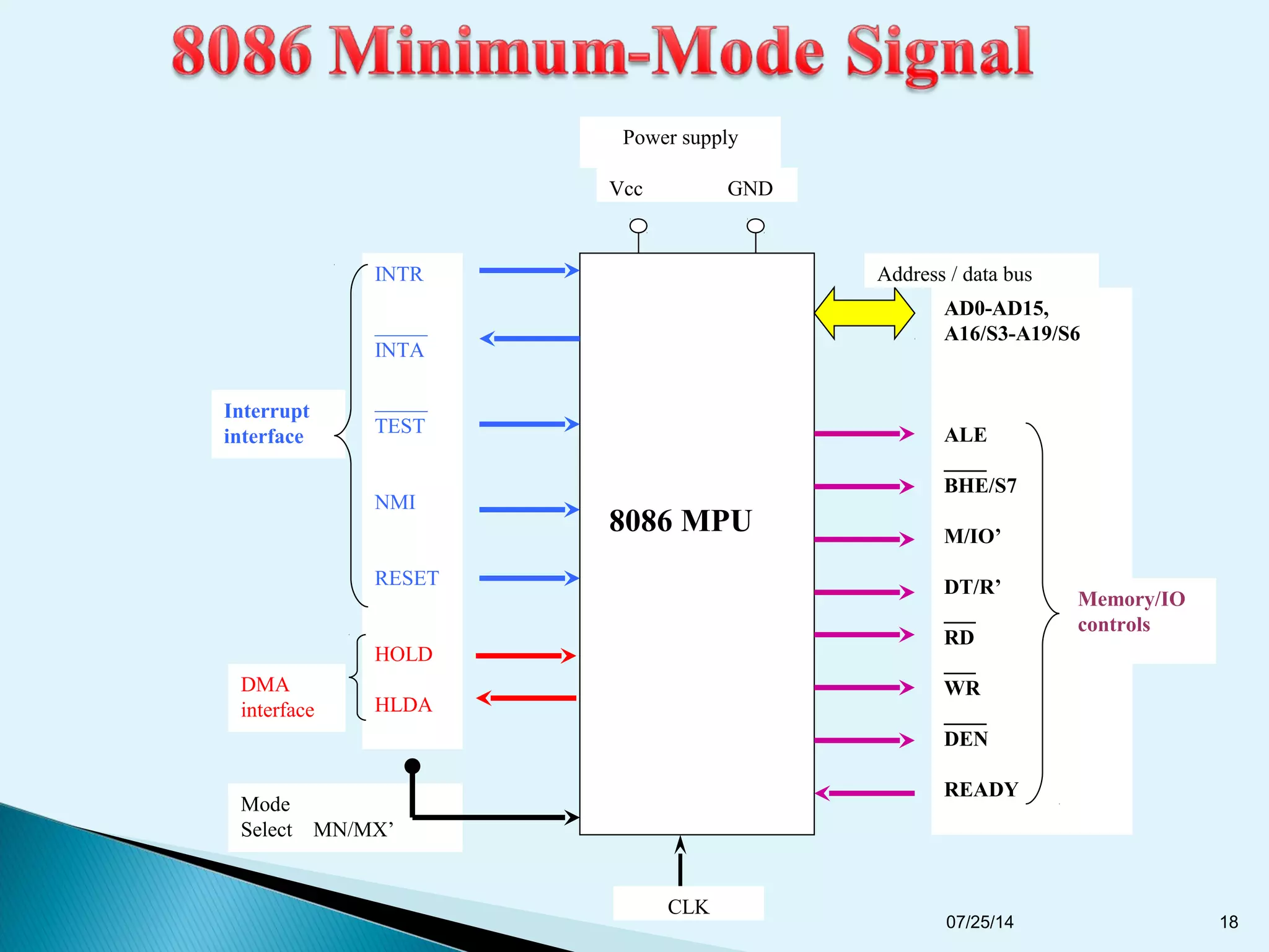
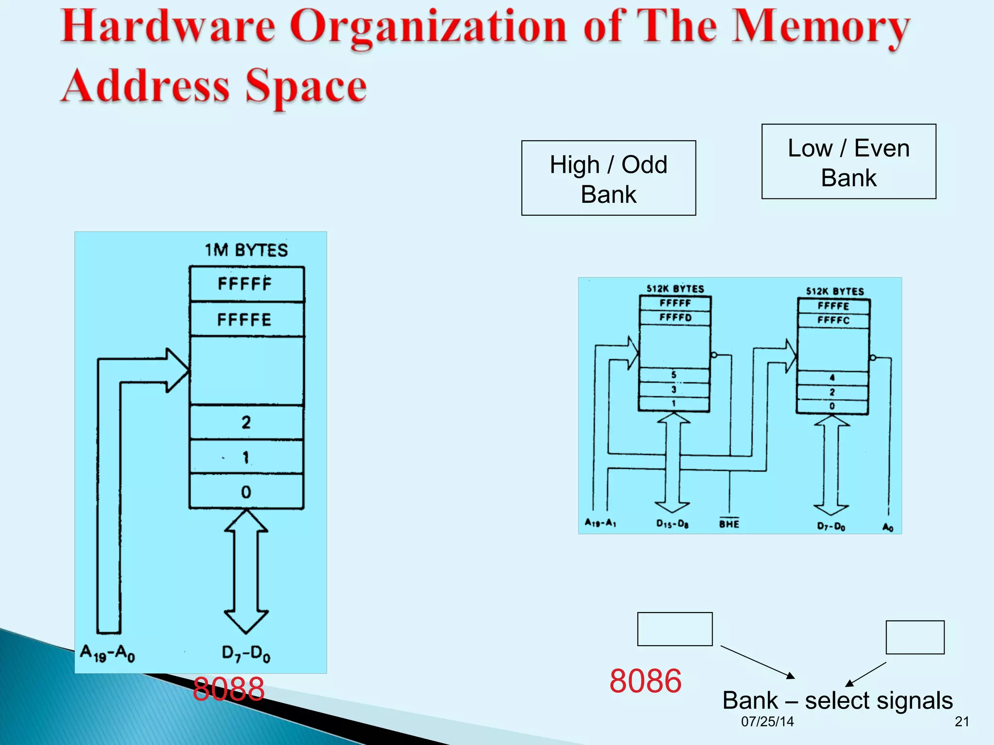
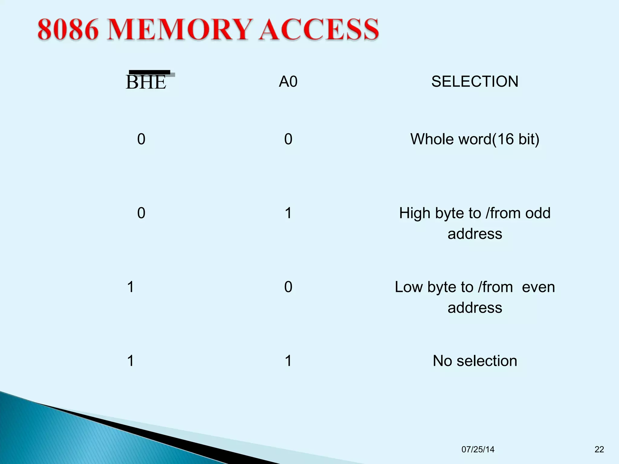
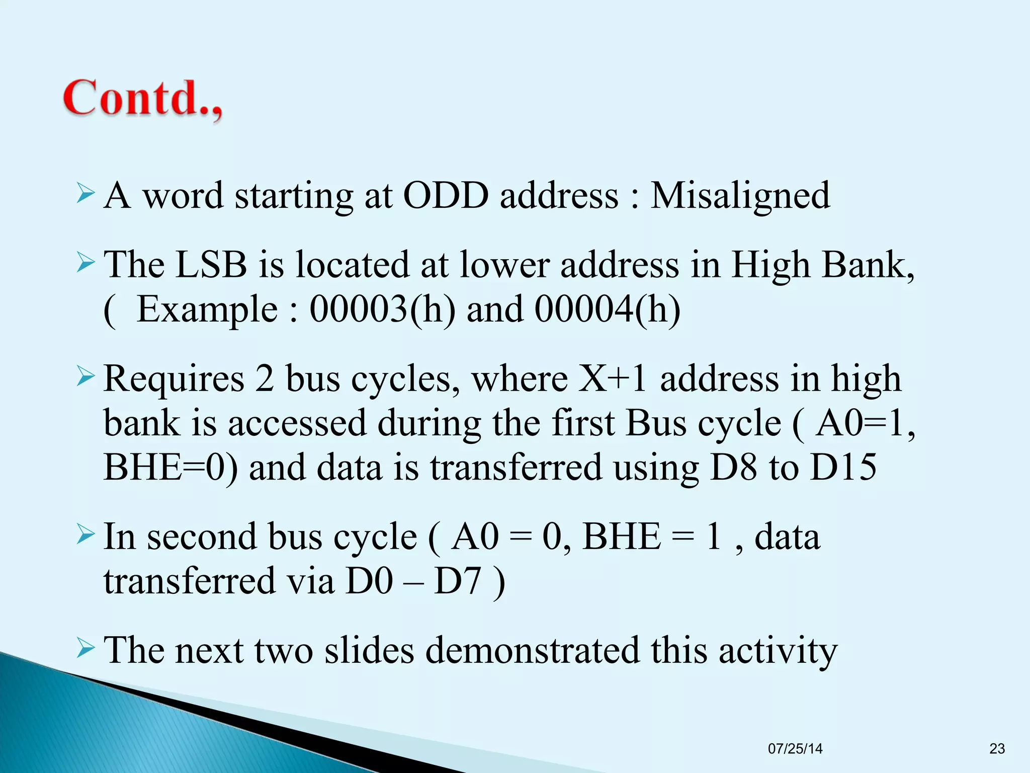
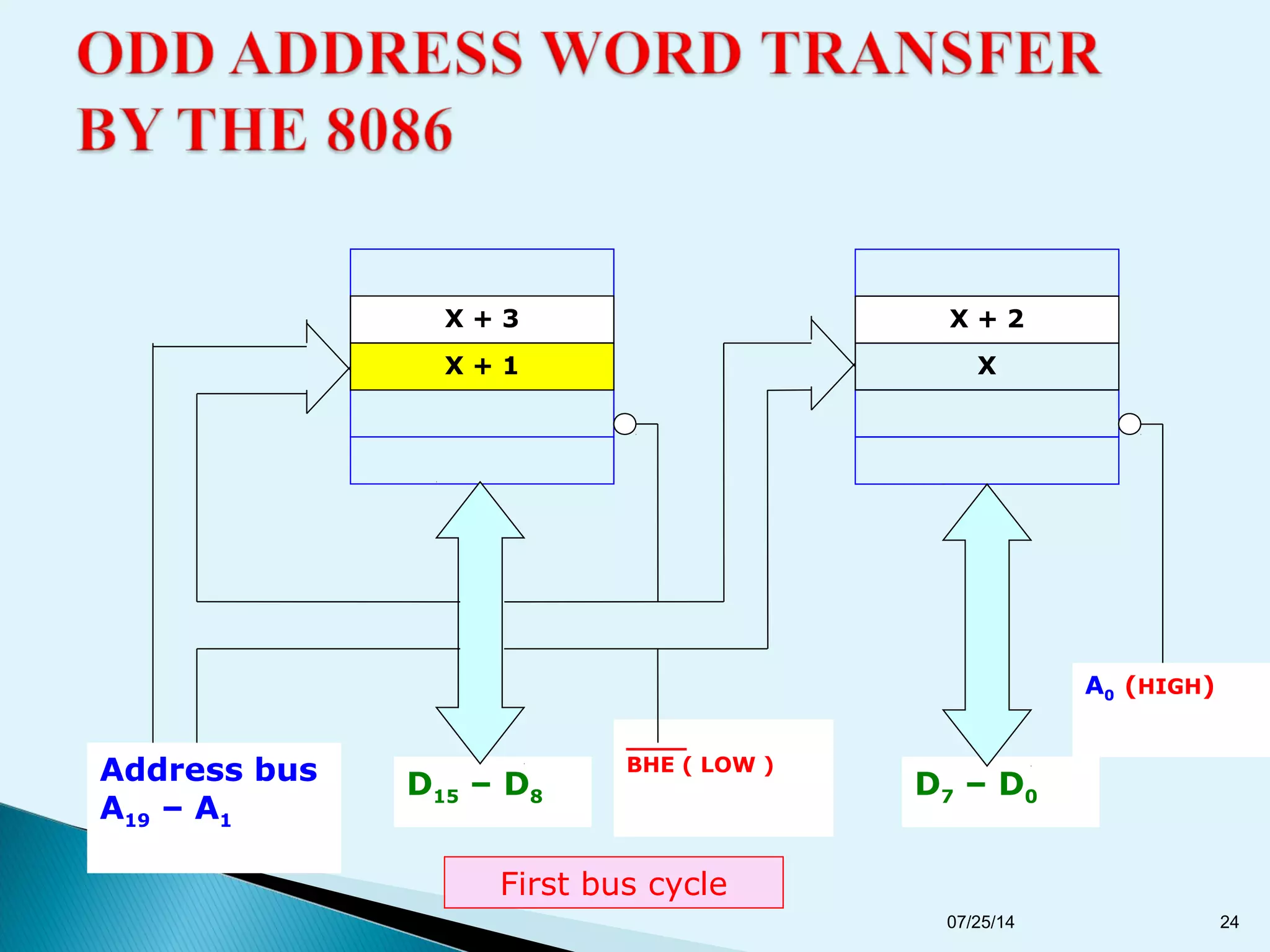
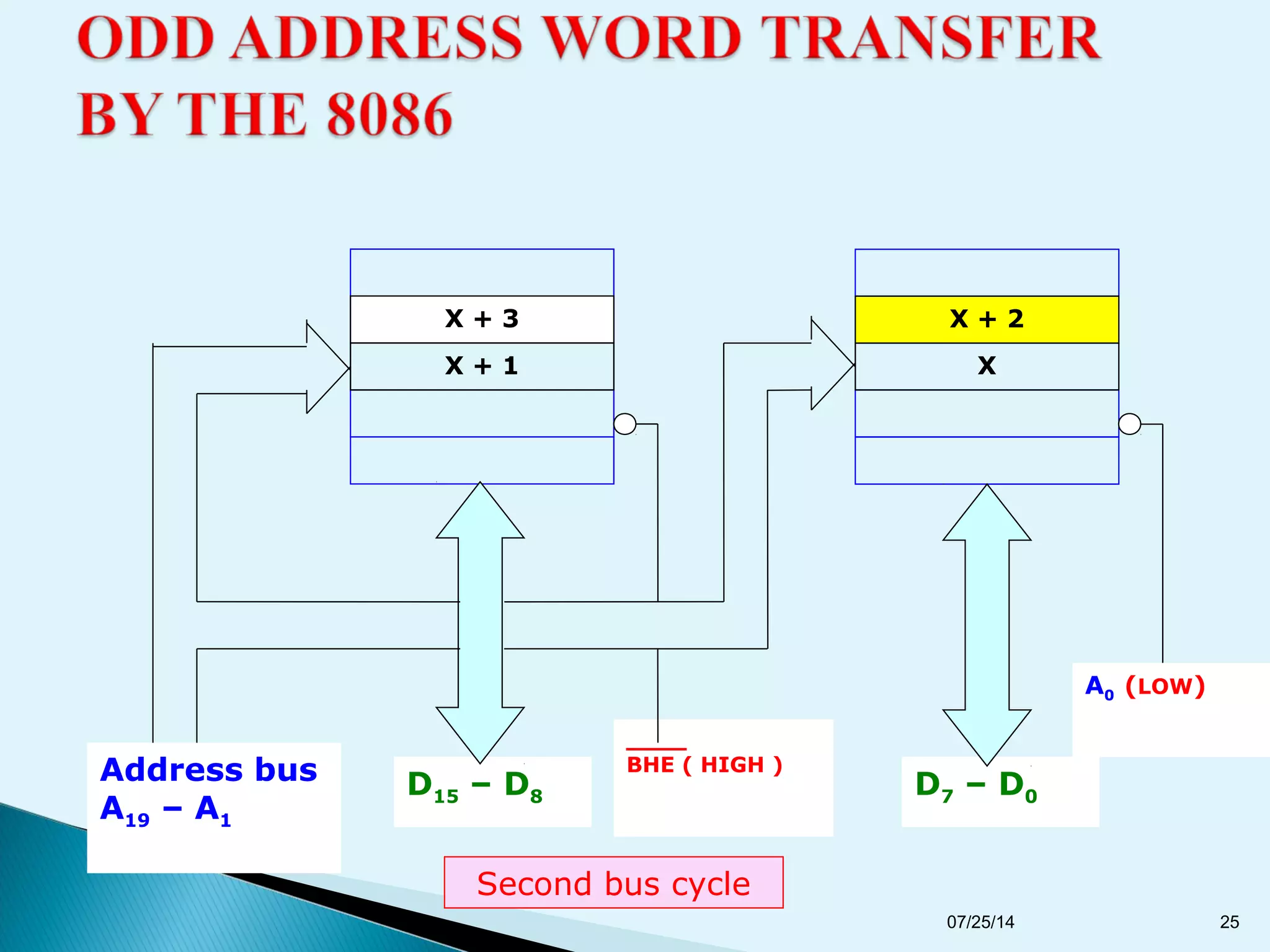
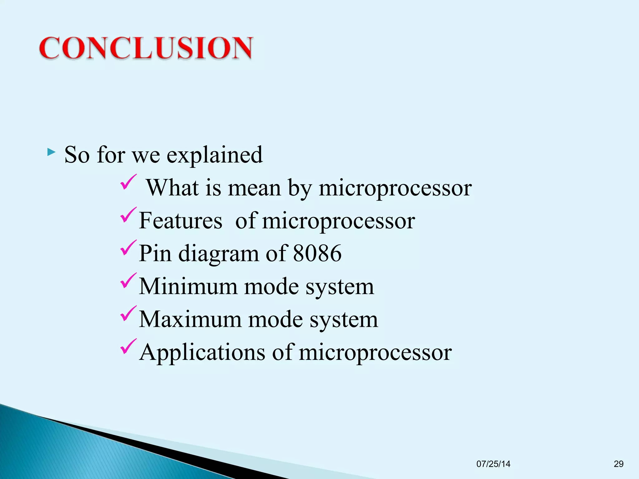
PRESENTED BY
K.DHARANI(MCA12004)
P.LAVANYA(MCA12011)
P.RAJESWARI(MCA12022)
T.SARANYA(MCA12027)
R.SWATHIKA(MCA12034)
GUIDED BY
Mrs.V.NIRMALA ME.,
(ASSISTENT PROFESSOR/ECE)07/25/14 1
 Microprocessor 8086
 Features of 8086
 Pin-diagram for 8086
 Minimum and Maximum mode systems
 Hardware organization
 Applications of 8086
07/25/14 2
07/25/14 3
07/25/14 5
07/25/14 6
07/25/14 7
07/25/14 8
07/25/14 9
HLDA
 It is hold acknowledge active signal.
 It is also an output signals and works like 8085
microprocessor .
HOLD
 It is the hold request signal which is used in DMA
to hold the system.
Request given to hold.
07/25/14 10
WR
It indicates the performance of the processor by
means of writing the memory or I/O operations.
It act in low signal.
M / IO
 It is the memory/input signal which is an O/P three
state signals.
 It is useful in distinguishing the memory access
from an I/O access.
07/25/14 11
DT/ R
 It is the data transmit/receive signal which
is also the three state O/P.
 It is useful for controlling the data and low
direction via transceiver.
DEN
 Is the data transmit/receive signal which is also the
three state O/P.
It is useful for controlling the data and low
direction via transceiver.
It both data transmit and receives.
07/25/14 12
ALE
Address Latch Enable
It is useful in demultiplexing.
INTA
 It is an output signal.
It is associated with INTR signal used for
aknowledgement of an interrupt by request.
07/25/14 13
Transceiver
 It works on behalf of the processor to transmit or
receive the data between memory and the
processor.
Latches
It is used to store the address that is supplied to
memory or I/O devices during the current machine
cycle.
Clock generator
The clock generator generates clock pluse for the
crystal is connected.
07/25/14 14
MEMORY AND I/O DEVICES
 The temporary data are usually stored in RAM.
It is used during execution of the program while
the permanent data are stored in PROM.
 The I/O devices are used to connect the
microprocessor with external I/P devices, which are
used to get the data and output devices.
It is used to send the data.
07/25/14 15
Advantages of Minimum Modes
It is cheap.
Microprocessor does itself generator I/O.
Microprocessor does itself generator I/O control
signal.
07/25/14 16
M/IO WR RD OPERATION
0 0 1 I/O write
0 1 0 I/O read
1 0 1 Memory write
1 1 0 Memory read
07/25/14 17
Mode
Select MN/MX’
Interrupt
interface
8086 MPU
Power supply
Vcc GND
INTR
_____
INTA
_____
TEST
NMI
RESET
HOLD
HLDA
Address / data bus
AD0-AD15,
A16/S3-A19/S6
ALE
____
BHE/S7
M/IO’
DT/R’
___
RD
___
WR
____
DEN
READY
CLK
DMA
interface
Memory/IO
controls
07/25/14 18
Clock (CLK) :
 Input signal which synchronize the internal and
external operations of the microprocessor.
8088 operates at two different speeds;
-5MHz <-standard ports.
-8MHz <- standard ports.
8086 Manufactured three speed:
 -5 MHz for standard 8086
-8 MHz for standard 8086-2
-10 MHz for standard 8086-1
07/25/14 19
The maximum mode signals are
RQ/GT0
It is requested/grant access control signals is
bidirectional in nature.
LOCK
 It is the output 3-state signal used for the purpose
of holding the operation
S2-S0
 S2-S0 are the output 32-state signal used for the
purpose of bus cycle status.
QS1,QS0
 QS1,QS0 are the output signal used for the purpose
of instruction queue status. 07/25/14 20
8088 8086
Low / Even
Bank
High / Odd
Bank
Bank – select signals
07/25/14 21
BHE A0 SELECTION
0 0 Whole word(16 bit)
0 1 High byte to /from odd
address
1 0 Low byte to /from even
address
1 1 No selection
07/25/14 22
 A word starting at ODD address : Misaligned
 The LSB is located at lower address in High Bank,
( Example : 00003(h) and 00004(h)
 Requires 2 bus cycles, where X+1 address in high
bank is accessed during the first Bus cycle ( A0=1,
BHE=0) and data is transferred using D8 to D15
 In second bus cycle ( A0 = 0, BHE = 1 , data
transferred via D0 – D7 )
 The next two slides demonstrated this activity
07/25/14 23
Address bus
A19 – A1
D15 – D8 D7 – D0
____
BHE ( LOW )
X + 2X + 3
X + 1 X
A0 (HIGH)
First bus cycle
07/25/14 24
Address bus
A19 – A1
D15 – D8 D7 – D0
____
BHE ( HIGH )
X + 2X + 3
X + 1 X
A0 (LOW)
Second bus cycle
07/25/14 25
Idle State:
 No bus activity required
Each is 1 clock period long
 Occurs when instruction queue is full or the MPU
does not need to read/write to memory
Wait State
Triggered by events external to MPU
 Buffer full will trigger a wait state
 Triggered by READY pin
 Inserted between T3 and T4
07/25/14 26
 It is used for various instruction set and interrupt
systems also.
 They were a popular, early, microprocessor
commonly embedded in washing machines and
domestic appliances, to replace mechanical timers
and interlocks.
 Home Appliances
 Air conditioner circuits
Telephone communication circuits
Fan Circuits
07/25/14 27
Induction cooker circuits
Lamp/ Lantern circuits
Refrigerator circuits
Television circuits
 Agricultural Automation Circuits
 Anti-harm circuits
Cultivation circuits
General circuits
 Electronic Maintenance circuits
 Remote control based circuits
 Networking circuits
 Telephone communication circuits
07/25/14 28
 So for we explained
 What is mean by microprocessor
Features of microprocessor
Pin diagram of 8086
Minimum mode system
Maximum mode system
Applications of microprocessor
07/25/14 29
 Advanced Microprocessors And Peripherals- AK
RAY & KM BHURCHANDI
 WEBSITES
 http://microprocessorforyou.blogspot.in/2011/12/feat
ures-of-8086.html
 http://8085projects.info/page/agricultural-
automation-circuits.html
07/25/14 30
““SUCCESS CANNOT BE ASSURED.SUCCESS CANNOT BE ASSURED.
IT MUST BE ATTAINED”.IT MUST BE ATTAINED”.
07/25/14 31
Minimum And Maximum Modes Of 80826

Minimum And Maximum Modes Of 80826

  • 1.
  • 2.
     Microprocessor 8086 Features of 8086  Pin-diagram for 8086  Minimum and Maximum mode systems  Hardware organization  Applications of 8086 07/25/14 2
  • 3.
  • 5.
  • 6.
  • 7.
  • 8.
  • 9.
  • 10.
    HLDA  It ishold acknowledge active signal.  It is also an output signals and works like 8085 microprocessor . HOLD  It is the hold request signal which is used in DMA to hold the system. Request given to hold. 07/25/14 10
  • 11.
    WR It indicates theperformance of the processor by means of writing the memory or I/O operations. It act in low signal. M / IO  It is the memory/input signal which is an O/P three state signals.  It is useful in distinguishing the memory access from an I/O access. 07/25/14 11
  • 12.
    DT/ R  Itis the data transmit/receive signal which is also the three state O/P.  It is useful for controlling the data and low direction via transceiver. DEN  Is the data transmit/receive signal which is also the three state O/P. It is useful for controlling the data and low direction via transceiver. It both data transmit and receives. 07/25/14 12
  • 13.
    ALE Address Latch Enable Itis useful in demultiplexing. INTA  It is an output signal. It is associated with INTR signal used for aknowledgement of an interrupt by request. 07/25/14 13
  • 14.
    Transceiver  It workson behalf of the processor to transmit or receive the data between memory and the processor. Latches It is used to store the address that is supplied to memory or I/O devices during the current machine cycle. Clock generator The clock generator generates clock pluse for the crystal is connected. 07/25/14 14
  • 15.
    MEMORY AND I/ODEVICES  The temporary data are usually stored in RAM. It is used during execution of the program while the permanent data are stored in PROM.  The I/O devices are used to connect the microprocessor with external I/P devices, which are used to get the data and output devices. It is used to send the data. 07/25/14 15
  • 16.
    Advantages of MinimumModes It is cheap. Microprocessor does itself generator I/O. Microprocessor does itself generator I/O control signal. 07/25/14 16
  • 17.
    M/IO WR RDOPERATION 0 0 1 I/O write 0 1 0 I/O read 1 0 1 Memory write 1 1 0 Memory read 07/25/14 17
  • 18.
    Mode Select MN/MX’ Interrupt interface 8086 MPU Powersupply Vcc GND INTR _____ INTA _____ TEST NMI RESET HOLD HLDA Address / data bus AD0-AD15, A16/S3-A19/S6 ALE ____ BHE/S7 M/IO’ DT/R’ ___ RD ___ WR ____ DEN READY CLK DMA interface Memory/IO controls 07/25/14 18
  • 19.
    Clock (CLK) : Input signal which synchronize the internal and external operations of the microprocessor. 8088 operates at two different speeds; -5MHz <-standard ports. -8MHz <- standard ports. 8086 Manufactured three speed:  -5 MHz for standard 8086 -8 MHz for standard 8086-2 -10 MHz for standard 8086-1 07/25/14 19
  • 20.
    The maximum modesignals are RQ/GT0 It is requested/grant access control signals is bidirectional in nature. LOCK  It is the output 3-state signal used for the purpose of holding the operation S2-S0  S2-S0 are the output 32-state signal used for the purpose of bus cycle status. QS1,QS0  QS1,QS0 are the output signal used for the purpose of instruction queue status. 07/25/14 20
  • 21.
    8088 8086 Low /Even Bank High / Odd Bank Bank – select signals 07/25/14 21
  • 22.
    BHE A0 SELECTION 00 Whole word(16 bit) 0 1 High byte to /from odd address 1 0 Low byte to /from even address 1 1 No selection 07/25/14 22
  • 23.
     A wordstarting at ODD address : Misaligned  The LSB is located at lower address in High Bank, ( Example : 00003(h) and 00004(h)  Requires 2 bus cycles, where X+1 address in high bank is accessed during the first Bus cycle ( A0=1, BHE=0) and data is transferred using D8 to D15  In second bus cycle ( A0 = 0, BHE = 1 , data transferred via D0 – D7 )  The next two slides demonstrated this activity 07/25/14 23
  • 24.
    Address bus A19 –A1 D15 – D8 D7 – D0 ____ BHE ( LOW ) X + 2X + 3 X + 1 X A0 (HIGH) First bus cycle 07/25/14 24
  • 25.
    Address bus A19 –A1 D15 – D8 D7 – D0 ____ BHE ( HIGH ) X + 2X + 3 X + 1 X A0 (LOW) Second bus cycle 07/25/14 25
  • 26.
    Idle State:  Nobus activity required Each is 1 clock period long  Occurs when instruction queue is full or the MPU does not need to read/write to memory Wait State Triggered by events external to MPU  Buffer full will trigger a wait state  Triggered by READY pin  Inserted between T3 and T4 07/25/14 26
  • 27.
     It isused for various instruction set and interrupt systems also.  They were a popular, early, microprocessor commonly embedded in washing machines and domestic appliances, to replace mechanical timers and interlocks.  Home Appliances  Air conditioner circuits Telephone communication circuits Fan Circuits 07/25/14 27
  • 28.
    Induction cooker circuits Lamp/Lantern circuits Refrigerator circuits Television circuits  Agricultural Automation Circuits  Anti-harm circuits Cultivation circuits General circuits  Electronic Maintenance circuits  Remote control based circuits  Networking circuits  Telephone communication circuits 07/25/14 28
  • 29.
     So forwe explained  What is mean by microprocessor Features of microprocessor Pin diagram of 8086 Minimum mode system Maximum mode system Applications of microprocessor 07/25/14 29
  • 30.
     Advanced MicroprocessorsAnd Peripherals- AK RAY & KM BHURCHANDI  WEBSITES  http://microprocessorforyou.blogspot.in/2011/12/feat ures-of-8086.html  http://8085projects.info/page/agricultural- automation-circuits.html 07/25/14 30
  • 31.
    ““SUCCESS CANNOT BEASSURED.SUCCESS CANNOT BE ASSURED. IT MUST BE ATTAINED”.IT MUST BE ATTAINED”. 07/25/14 31