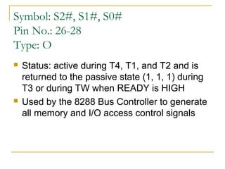
Downloaded 832 times

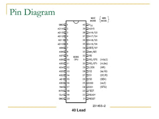
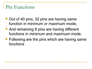
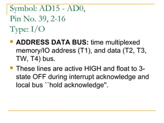
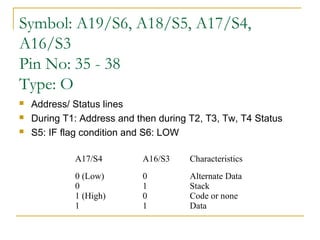
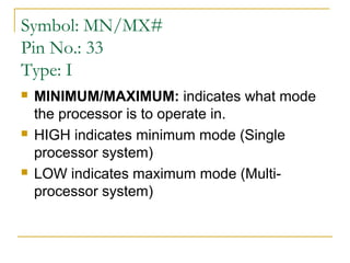
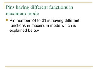
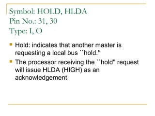


This document describes the pin functions of the Intel 8086 microprocessor. It explains that 32 pins have the same functions in minimum and maximum mode, while 8 pins have different functions depending on the mode. It provides details on the pin symbols, numbers, types, and functions for address bus lines, status lines, control lines for reading, writing, interrupts, and more. The pins with differing functions in minimum and maximum modes are also described.