3dchips
•
1 like•889 views
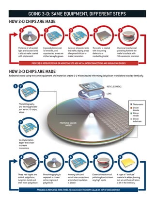
The document compares the processes for making 2D and 3D chips. For 2D chips, patterns of UV light are focused on a silicon wafer coated with photoresist, exposed areas are etched away, and ions are showered on to dope silicon and make transistors. The process is repeated 4+ times to add metal interconnects and insulators. For 3D chips, the same equipment and materials are used, but additional steps stack polysilicon transistors vertically by repeating photolithography and etching to create active polysilicon regions and adding new layers like polysilicon, tungsten, and antifuse material. The 3D process is repeated 9 times to stack 8 memory cells.
Report
Share
Report
Share
Recommended
Fabrication process of Integrated Circuit (IC's)
The document discusses the process of fabricating integrated circuits (ICs). It involves:
1. Creating a silicon wafer through crystal growth and polishing.
2. Using photolithography and etching to selectively remove silicon and create circuit patterns on the wafer.
3. Adding dopants to the wafer through diffusion or ion implantation to create transistors and other components.
4. Depositing layers of metal and dielectric materials and etching interconnects to connect the components.
5. Cutting the wafer into individual chips, testing them, and packaging in protective enclosures. The process requires multiple sequential steps of deposition, doping, etching, and testing.
Device isolation Techniques
The document discusses various techniques for electrically isolating devices in integrated circuits. It describes junction isolation, which uses reverse biased PN junctions, but this did not scale well as devices became smaller. Dielectric isolation techniques like LOCOS and STI were developed using deposited or thermally grown oxides. LOCOS had limitations like bird's beak encroachment affecting small device areas. STI involves etching trenches and depositing oxide to fill them, avoiding issues with LOCOS at small scales.
Wafer preparation
This document discusses the preparation process for silicon wafers used in integrated circuit manufacturing. It describes how a silicon crystal is grown and cut into wafers, which then undergo cleaning, etching, planarization, polishing, and inspection steps to produce a smooth, flat surface suitable for microfabrication. Key properties of wafers that are controlled include diameter, thickness, bow, thickness variation, and surface orientation. The presentation concludes that wafers serve as substrates for building microelectronic devices and undergo many process steps before individual circuits are separated and packaged.
Wafer Fabrication, CZ Method--ABU SYED KUET
Crystal structures can be single crystal, polycrystalline, or amorphous. Single crystal silicon is used to manufacture solar cells and semiconductors due to its precise electronic properties. The Czochralski method is commonly used to grow large single crystal silicon ingots from melted, purified silicon in quartz crucibles. The ingots are sliced, polished, and cleaned to produce thin round wafers for semiconductor fabrication. Larger diameter wafers allow more chips to be produced from each wafer, increasing manufacturing efficiency.
MOSFET fabrication 12
The document discusses the fabrication process of MOSFET transistors. It begins by introducing common semiconductor materials like silicon and compound semiconductors. Lithography is then described as the process of selectively patterning layers using a photomask and photoresist. The basic CMOS fabrication process involves growing oxide layers, creating wells, depositing polysilicon for gates, and doping the source and drain regions. Specifically, the n-MOS transistor fabrication process is outlined, showing the steps of oxidizing silicon, patterning field oxide, depositing gate oxide and polysilicon, doping the source and drain areas, and finally depositing contacts and interconnects.
Device isolation
This document discusses two main techniques for isolating transistors in semiconductor fabrication: LOCOS (Local Oxidation of Silicon) and STI (Shallow Trench Isolation). LOCOS uses a thermal oxidation process which results in a "bird's beak" encroachment that wastes surface area. STI improves on LOCOS by etching shallow trenches and filling them with deposited oxide, avoiding the bird's beak effect but requiring more processing steps. Both techniques utilize thermally grown oxides and masks like silicon nitride to selectively grow isolation oxides and define active device areas.
Lect5 Diffusion
The key processes involved in IC manufacturing on the wafer include diffusion, ion implantation, photolithography, deposition, and etching. Specifically, diffusion and ion implantation are used to introduce impurities into silicon to control conductivity by either thermal diffusion of dopant atoms into silicon or injection of energetic dopant ions. Fick's first and second laws of diffusion describe diffusion quantitatively, where the flux of diffusing particles is proportional to the concentration gradient according to the first law, and the second law relates the change in concentration over time to the divergence of the flux.
Wafer manufacturing process
The document describes the key steps in the semiconductor manufacturing process including silicon manufacturing using the Czochralski method, photolithography using photoresists and photomasks, and ion implantation. Photolithography involves coating wafers with photoresist, exposing it to light through a photomask, and developing the resist to transfer patterns. Ion implantation injects dopants by accelerating ions toward the wafer surface.
Fabrication steps of IC
The document provides an overview of integrated circuit fabrication processes. It discusses the basic steps including wafer production, epitaxial growth, etching, masking, doping, diffusion, implantation, and metallization. It also describes the fabrication processes for MOSFETs including NMOS, PMOS and CMOS. BiCMOS fabrication is also summarized, which combines BJT and CMOS processes to achieve high speed and low power benefits.
Flexible Electronics PPT by Sourabh Kumar
www.androroot.com
Flexible Electronics PPT by Sourabh Kumar for B.Tech final Year.Set of 25 Slides with proper images and Lots of Examples.
VLSI Design(Fabrication)
this ppt provides fabrication on SI wafer, CMOS fabrication process, basic CMOS inverter, future, application, advantage, disadvantage etc.
Lithography fabrication ppt
Lithography is a process that uses light to transfer geometric patterns from a photomask to a light-sensitive chemical "photoresist" on a semiconductor substrate. The key steps in the lithography process include cleaning and preparing the wafer surface, depositing and spinning photoresist, soft baking to evaporate solvents, aligning the mask and exposing the photoresist to light, developing to remove exposed or unexposed areas of photoresist, hard baking to harden the photoresist, plasma etching or depositing additional layers, cleaning, and inspecting the final patterned wafer. Lithography is critical for manufacturing integrated circuits and is capable of printing ever smaller semiconductor features.
A brief description of photolithography
Photolithography is a technique used to transfer geometric patterns from a photomask to a photoresist layer on a substrate. It involves cleaning the substrate, coating it with photoresist, exposing the photoresist to light through a photomask, developing the photoresist to remove either exposed or unexposed areas, etching the substrate where the photoresist was removed, and stripping off the remaining photoresist. Photolithography is widely used in the semiconductor industry to fabricate microelectronic circuits and sensors.
IC Fabrication Process
Semiconductor device fabrication is the process used to create the integrated circuits that are present in everyday electrical and electronic devices. It is a multiple-step sequence of photo lithographic and chemical processing steps during which electronic circuits are gradually created on a wafer made of pure semiconducting material. Silicon is almost always used, but various compound semiconductors are used for specialized applications.
Ion implantation VLSI
Ion implantation is a process used to dope semiconductors by bombarding them with ions. It allows independent control of dopant profile and concentration. Ions are ionized from source gases, accelerated, selected by mass, and implanted into wafers. Implanted ions damage the crystal structure which is repaired by annealing. Ion implantation offers anisotropic doping, low temperature processing, and precise doping levels compared to diffusion.
Optical switching
Optical switches enable signals in optical fibers or integrated optical circuits to be selectively switched from one circuit to another. They operate using mechanical means such as physically shifting fibers, or electro-optic, magneto-optic, or other methods. Optical switches can be slow, for alternate routing around faults, or fast, for logic operations using electro-optic or magneto-optic effects. Optical networks transmit data digitally as light through connected fiber strands and include SDH/SONET, opaque, partially transparent, and all-optical networks. All-optical networks perform all operations and functions optically without opto-electronics conversion.
CMOS LOGIC STRUCTURES
This presentation has given a brief introduction and working of CMOS Logic Structures which includes MOS logic, CMOS logic, CMOS logic structure, CMOS complementary logic, pass transistor logic, bi CMOS logic, pseudo –nMOS logic, CMOS domino logic, Cascode Voltage Switch Logic(CVSL), clocked CMOS logic(c²mos), dynamic CMOS logic
Oxidation
This document discusses oxidation in semiconductor device fabrication. It describes oxidation as the process of converting silicon into silicon dioxide, which can occur through dry oxidation using oxygen or wet oxidation using water/steam at high temperatures from 900-1200°C. The key functions of the resulting silicon dioxide layer include acting as a diffusion mask, providing surface passivation and insulation, and enabling device isolation in integrated circuits. The document also classifies oxidation as either diffusion limited or reaction controlled depending on oxide thickness and oxidation time.
Silicon on Insulator (SOI) Technology
This presentation discusses about the concept of SOI technology, Fabrication methods, applications, advantages and limitations of SOI technology.
integrated circuit febrication
Integrated circuits (ICs) are microscopic arrays of electronic components integrated onto a single chip of semiconductor material. There are several types of ICs based on their structure and fabrication method. Thick and thin film ICs are formed on an insulating substrate using screen printing or vacuum deposition techniques and can contain resistors, capacitors, and inductors but not transistors or diodes. Monolithic ICs integrate all components onto a single silicon wafer using photolithography to diffusively dope regions of the wafer with impurities. Hybrid ICs combine monolithic and thick/thin film fabrication by first forming transistors on a silicon wafer, covering it with an insulating layer, and then adding passive film components and interconnecting them to the underlying
Crystal Growth
The document discusses the process of manufacturing single crystal silicon ingots for use in semiconductor chips. Raw silicon is obtained from sand and purified to electronic grade silicon. Single crystals are formed using techniques like the Czochralski method, where a silicon seed crystal is pulled slowly from a melt of purified silicon. This allows the silicon atoms to align uniformly and form a single crystal ingot. The ingots are sliced into thin wafers that serve as the base material for etching circuits onto semiconductor chips.
Power dissipation cmos
This document discusses power dissipation in CMOS circuits. It identifies the main sources of power dissipation as dynamic, static, and short circuit power. Dynamic power is caused by charging and discharging capacitors during switching and depends on activity factors, voltage, and frequency. Static power includes leakage currents that occur even when the device is inactive. Short circuit power arises when both NMOS and PMOS are on simultaneously during signal transitions. The document provides techniques for reducing each type of power dissipation such as lowering voltage, reducing switching activity, minimizing capacitance and transistor sizing.
Design and development of carry select adder
DESIGN AND DEVELOPMENT OF DIFFERENT TYPE OF CARRY SELECT ADDER AND IMPLEMENTED USING VERING IN XILINX ISE 14.7 AND COMPARE THEM TO FIND EFFICIENT CSLA
Cmos fabrication process
The CMOS fabrication process in VLSI.
CMOS (complementary metal-oxide-semiconductor) is the term usually used to describe the small amount of memory on a computer motherboard that stores the BIOS settings.
Ic tech unit 5- VLSI Process Integration
junction oxide and isolation techniques, LOCOS, Metallization, NMOS and CMOS technology, FAult diagnosis
Vapor Phase Deposition Techniques
Vapor phase deposition is a technique used to prepare pure optical glasses. It involves vaporizing inorganic compounds and dopants and depositing them as thin films on a substrate through chemical reactions, forming a porous soot preform. The preform is then consolidated through heating to become a solid glass cylinder that can be drawn into an optical fiber. Common vapor deposition methods include outside vapor phase oxidation, vapor axial deposition, modified chemical vapor deposition, and plasma-activated chemical vapor deposition. These processes allow producing silica-based fibers with very low light attenuation and optimal optical properties.
Ion beam lithography
The document discusses ion-beam lithography, which uses a focused beam of ions instead of electrons or photons to pattern surfaces. Ion-beam lithography offers higher resolution than other lithography techniques due to ions having higher momentum and less scattering. It can define patterns through physical sputtering, chemical reactions with precursor gases, or ion implantation. While having advantages like high resolution and minimal proximity effects, it also has lower throughput and can damage substrates more than other lithography methods. The document provides details on ion sources, lithography processes, advantages and disadvantages of the technique.
Plankton Forest
- Marine phytoplankton play a key role in regulating Earth's climate by absorbing large amounts of carbon dioxide from the atmosphere and oceans through photosynthesis.
- Using satellite data and improved models, scientists have learned that phytoplankton absorb nearly as much carbon globally as all land plants, and about 15% of the carbon absorbed by phytoplankton each year is transported deep into the ocean via the "biological pump."
- Some scientists have proposed artificially enhancing phytoplankton growth through ocean iron fertilization as a means to mitigate climate change, but the environmental impacts of such large-scale manipulation are still uncertain and debated.
Einsteinin Trouble
Creative solution to very difficult concepts, Quantum Mechanics and Special Relativity
More Related Content
What's hot
Fabrication steps of IC
The document provides an overview of integrated circuit fabrication processes. It discusses the basic steps including wafer production, epitaxial growth, etching, masking, doping, diffusion, implantation, and metallization. It also describes the fabrication processes for MOSFETs including NMOS, PMOS and CMOS. BiCMOS fabrication is also summarized, which combines BJT and CMOS processes to achieve high speed and low power benefits.
Flexible Electronics PPT by Sourabh Kumar
www.androroot.com
Flexible Electronics PPT by Sourabh Kumar for B.Tech final Year.Set of 25 Slides with proper images and Lots of Examples.
VLSI Design(Fabrication)
this ppt provides fabrication on SI wafer, CMOS fabrication process, basic CMOS inverter, future, application, advantage, disadvantage etc.
Lithography fabrication ppt
Lithography is a process that uses light to transfer geometric patterns from a photomask to a light-sensitive chemical "photoresist" on a semiconductor substrate. The key steps in the lithography process include cleaning and preparing the wafer surface, depositing and spinning photoresist, soft baking to evaporate solvents, aligning the mask and exposing the photoresist to light, developing to remove exposed or unexposed areas of photoresist, hard baking to harden the photoresist, plasma etching or depositing additional layers, cleaning, and inspecting the final patterned wafer. Lithography is critical for manufacturing integrated circuits and is capable of printing ever smaller semiconductor features.
A brief description of photolithography
Photolithography is a technique used to transfer geometric patterns from a photomask to a photoresist layer on a substrate. It involves cleaning the substrate, coating it with photoresist, exposing the photoresist to light through a photomask, developing the photoresist to remove either exposed or unexposed areas, etching the substrate where the photoresist was removed, and stripping off the remaining photoresist. Photolithography is widely used in the semiconductor industry to fabricate microelectronic circuits and sensors.
IC Fabrication Process
Semiconductor device fabrication is the process used to create the integrated circuits that are present in everyday electrical and electronic devices. It is a multiple-step sequence of photo lithographic and chemical processing steps during which electronic circuits are gradually created on a wafer made of pure semiconducting material. Silicon is almost always used, but various compound semiconductors are used for specialized applications.
Ion implantation VLSI
Ion implantation is a process used to dope semiconductors by bombarding them with ions. It allows independent control of dopant profile and concentration. Ions are ionized from source gases, accelerated, selected by mass, and implanted into wafers. Implanted ions damage the crystal structure which is repaired by annealing. Ion implantation offers anisotropic doping, low temperature processing, and precise doping levels compared to diffusion.
Optical switching
Optical switches enable signals in optical fibers or integrated optical circuits to be selectively switched from one circuit to another. They operate using mechanical means such as physically shifting fibers, or electro-optic, magneto-optic, or other methods. Optical switches can be slow, for alternate routing around faults, or fast, for logic operations using electro-optic or magneto-optic effects. Optical networks transmit data digitally as light through connected fiber strands and include SDH/SONET, opaque, partially transparent, and all-optical networks. All-optical networks perform all operations and functions optically without opto-electronics conversion.
CMOS LOGIC STRUCTURES
This presentation has given a brief introduction and working of CMOS Logic Structures which includes MOS logic, CMOS logic, CMOS logic structure, CMOS complementary logic, pass transistor logic, bi CMOS logic, pseudo –nMOS logic, CMOS domino logic, Cascode Voltage Switch Logic(CVSL), clocked CMOS logic(c²mos), dynamic CMOS logic
Oxidation
This document discusses oxidation in semiconductor device fabrication. It describes oxidation as the process of converting silicon into silicon dioxide, which can occur through dry oxidation using oxygen or wet oxidation using water/steam at high temperatures from 900-1200°C. The key functions of the resulting silicon dioxide layer include acting as a diffusion mask, providing surface passivation and insulation, and enabling device isolation in integrated circuits. The document also classifies oxidation as either diffusion limited or reaction controlled depending on oxide thickness and oxidation time.
Silicon on Insulator (SOI) Technology
This presentation discusses about the concept of SOI technology, Fabrication methods, applications, advantages and limitations of SOI technology.
integrated circuit febrication
Integrated circuits (ICs) are microscopic arrays of electronic components integrated onto a single chip of semiconductor material. There are several types of ICs based on their structure and fabrication method. Thick and thin film ICs are formed on an insulating substrate using screen printing or vacuum deposition techniques and can contain resistors, capacitors, and inductors but not transistors or diodes. Monolithic ICs integrate all components onto a single silicon wafer using photolithography to diffusively dope regions of the wafer with impurities. Hybrid ICs combine monolithic and thick/thin film fabrication by first forming transistors on a silicon wafer, covering it with an insulating layer, and then adding passive film components and interconnecting them to the underlying
Crystal Growth
The document discusses the process of manufacturing single crystal silicon ingots for use in semiconductor chips. Raw silicon is obtained from sand and purified to electronic grade silicon. Single crystals are formed using techniques like the Czochralski method, where a silicon seed crystal is pulled slowly from a melt of purified silicon. This allows the silicon atoms to align uniformly and form a single crystal ingot. The ingots are sliced into thin wafers that serve as the base material for etching circuits onto semiconductor chips.
Power dissipation cmos
This document discusses power dissipation in CMOS circuits. It identifies the main sources of power dissipation as dynamic, static, and short circuit power. Dynamic power is caused by charging and discharging capacitors during switching and depends on activity factors, voltage, and frequency. Static power includes leakage currents that occur even when the device is inactive. Short circuit power arises when both NMOS and PMOS are on simultaneously during signal transitions. The document provides techniques for reducing each type of power dissipation such as lowering voltage, reducing switching activity, minimizing capacitance and transistor sizing.
Design and development of carry select adder
DESIGN AND DEVELOPMENT OF DIFFERENT TYPE OF CARRY SELECT ADDER AND IMPLEMENTED USING VERING IN XILINX ISE 14.7 AND COMPARE THEM TO FIND EFFICIENT CSLA
Cmos fabrication process
The CMOS fabrication process in VLSI.
CMOS (complementary metal-oxide-semiconductor) is the term usually used to describe the small amount of memory on a computer motherboard that stores the BIOS settings.
Ic tech unit 5- VLSI Process Integration
junction oxide and isolation techniques, LOCOS, Metallization, NMOS and CMOS technology, FAult diagnosis
Vapor Phase Deposition Techniques
Vapor phase deposition is a technique used to prepare pure optical glasses. It involves vaporizing inorganic compounds and dopants and depositing them as thin films on a substrate through chemical reactions, forming a porous soot preform. The preform is then consolidated through heating to become a solid glass cylinder that can be drawn into an optical fiber. Common vapor deposition methods include outside vapor phase oxidation, vapor axial deposition, modified chemical vapor deposition, and plasma-activated chemical vapor deposition. These processes allow producing silica-based fibers with very low light attenuation and optimal optical properties.
Ion beam lithography
The document discusses ion-beam lithography, which uses a focused beam of ions instead of electrons or photons to pattern surfaces. Ion-beam lithography offers higher resolution than other lithography techniques due to ions having higher momentum and less scattering. It can define patterns through physical sputtering, chemical reactions with precursor gases, or ion implantation. While having advantages like high resolution and minimal proximity effects, it also has lower throughput and can damage substrates more than other lithography methods. The document provides details on ion sources, lithography processes, advantages and disadvantages of the technique.
What's hot (20)
Viewers also liked
Plankton Forest
- Marine phytoplankton play a key role in regulating Earth's climate by absorbing large amounts of carbon dioxide from the atmosphere and oceans through photosynthesis.
- Using satellite data and improved models, scientists have learned that phytoplankton absorb nearly as much carbon globally as all land plants, and about 15% of the carbon absorbed by phytoplankton each year is transported deep into the ocean via the "biological pump."
- Some scientists have proposed artificially enhancing phytoplankton growth through ocean iron fertilization as a means to mitigate climate change, but the environmental impacts of such large-scale manipulation are still uncertain and debated.
Einsteinin Trouble
Creative solution to very difficult concepts, Quantum Mechanics and Special Relativity
Immune Receptors
Toll-like receptors (TLRs) play an important role in the innate immune system by recognizing various pathogens like bacteria, viruses, and fungi. The 10 identified human TLRs each recognize distinct molecular patterns from different classes of pathogens. For example, TLR4 binds to LPS from gram-negative bacteria, TLR2 binds to lipoproteins from bacteria and GPI anchors from parasites, and TLR3 binds to double-stranded viral RNA. Together, TLRs can detect nearly every type of pathogen. Upon activation by their specific ligands, TLRs signal intracellularly to activate transcription factors that turn on genes encoding inflammatory cytokines, inducing innate immune responses and linking to the adaptive immune system.
Atherosclerosis
Atherosclerosis is a disease that causes chest pain, heart attacks, and strokes, and leads to more deaths than cancer. The traditional view of how it develops is wrong. It begins when excess LDL particles in the blood accumulate in the artery wall and undergo changes that cause inflammation. Immune cells are drawn to the area, where they release inflammatory molecules. Macrophages ingest the modified LDL, becoming foam cells that constitute early fatty streaks. Further growth of the plaque involves smooth muscle cells building a fibrous cap. However, enzymes and cytokines released by foam cells can weaken the cap, possibly causing it to rupture and form dangerous blood clots.
Modern Mind
The document discusses evidence that personal adornment and symbol use in early humans may have begun far earlier than previously thought, based on 75,000-year-old shell beads found in Blombos Cave in South Africa. This suggests that modern human behavior emerged much deeper in our evolutionary history than commonly believed, as other archaeological finds are pushing back dates for activities like long-distance trade, art, complex stone tool making, and other cultural practices. However, most experts agree that modern behaviors became more widespread after around 40,000 years ago.
Reuters: Pictures of the Year 2016 (Part 2)
This document contains 20 photos from news events around the world between January and November 2016. The photos show international events like the US presidential election, the conflict in Ukraine, the migrant crisis in Europe, the Rio Olympics, and more. They also depict human interest stories and natural phenomena from various countries.
The Six Highest Performing B2B Blog Post Formats
If your B2B blogging goals include earning social media shares and backlinks to boost your search rankings, this infographic lists the size best approaches.
The Outcome Economy
1) The document discusses the opportunity for technology to improve organizational efficiency and transition economies into a "smart and clean world."
2) It argues that aggregate efficiency has stalled at around 22% for 30 years due to limitations of the Second Industrial Revolution, but that digitizing transport, energy, and communication through technologies like blockchain can help manage resources and increase efficiency.
3) Technologies like precision agriculture, cloud computing, robotics, and autonomous vehicles may allow for "dematerialization" and do more with fewer physical resources through effects like reduced waste and need for transportation/logistics infrastructure.
Viewers also liked (8)
Similar to 3dchips
1393809.ppt
This document provides an overview of the process for manufacturing silicon wafers from raw materials. It begins with obtaining high purity silicon from quartz and producing polycrystalline silicon. The Czochralski process is used to grow silicon single crystals by pulling a seed crystal from a silicon melt. Critical parameters like temperature, pull rate and rotation are controlled. Wafers are then cut from the ingot and undergo multiple processing steps including grinding, polishing, and cleaning to produce finished silicon wafers for semiconductor manufacturing.
Manufacturing of microprocessor
The manufacturing of microprocessors involves growing pure silicon crystals, slicing wafers, and fabricating integrated circuits through repeated photolithography, etching, deposition, and doping steps in a clean room environment. Key steps include slicing silicon ingots into wafers, layering and patterning materials like insulators and conductors through photolithography and etching, and implanting dopants using ion implantation. After fabrication, the wafers are tested, cut into chips, and packaged into protective casings before use in electronic devices.
Lect2 up020 (100324)
The document discusses submicron CMOS technology. It begins by categorizing CMOS technology based on minimum feature size, including submicron, deep submicron, and ultra-deep submicron. It then covers fundamental IC process steps such as oxidation, diffusion, ion implantation, deposition, etching, and photolithography. Finally, it outlines the typical process steps for fabricating an n-well CMOS device, including growing field oxide, depositing polysilicon, and implanting source/drain regions.
vlsi fabrication
The document discusses the key process steps in integrated circuit fabrication. It describes (1) preparing silicon wafers through processes like growing silicon crystals from sand and cutting the crystals into wafers, (2) diffusing impurities like boron and phosphorus into the wafers through high-temperature processes to dope the silicon, and (3) implanting ions of desired impurities into the wafers through acceleration and bombardment. The document also covers other important steps like annealing to activate the dopants, oxidizing the silicon to form insulating silicon dioxide layers, and lithography among others.
Project process flow final
This document describes the fabrication process for general purpose gratings using sidewall image transfer technique. The process involves depositing and patterning silicon oxide, polysilicon/amorphous silicon, and silicon nitride layers on a silicon wafer using optical lithography and reactive ion etching. The pattern is transferred between layers to etch silicon gratings in the wafer with line widths below the resolution limit of optical lithography. The technique allows fabrication of sub-micron gratings using existing optical lithography equipment, making it industrially favorable over alternatives like e-beam lithography. Microscope images show successful transfer of patterns between layers and etching of gratings in silicon.
Making of a silicon chip
The document describes the 10-stage process by which sand is transformed into computer processor chips at Intel's factory. Stage 1 involves converting sand into high purity silicon ingots. Stage 2 grows a cylindrical silicon crystal using the Czochralski process. Stage 3 slices the crystal into thin wafers. Stages 4-6 create transistors on the wafers by doping, etching, and depositing layers. Stages 7-8 connect the transistors by etching tracks and layers. Stage 9 tests the chips. Stage 10 packages finished chips for use. The process requires over 300 steps to transform sand into complex processor components just 45 millionths of a millimeter in size.
Unit-6 Semiconductor Manufacturing Process.pptx
The document discusses integrated circuit fabrication processes. It introduces basic steps like oxidation, diffusion, ion implantation, deposition, etching, and epitaxy. Photolithography is used to apply these steps selectively through masking. The fabrication process involves growing thin oxides, doping silicon through diffusion or implantation, depositing materials, and selectively removing layers with etching. Top-down and bottom-up are two approaches, with top-down using masking and etching and bottom-up growing structures from seed crystals or polymers.
silicon ic fabrican technology
This document describes the process for fabricating a silicon integrated circuit. It begins with an overview of the basic steps, which include cleaning silicon wafers, oxidation, photolithography, etching, diffusion, thin film deposition, and testing. It then focuses on the specific process for fabricating a P-N junction diode, outlining 10 steps: cleaning, oxidation, photolithography, etching, diffusion, metal deposition, photolithography, etching, contact formation, and testing. Diagrams and descriptions are provided for each step in the P-N diode fabrication process.
Integrated circuits ic
Integrated circuits are formed on small silicon chips and can be categorized based on the number of logic gates as SSI, MSI, LSI, VLSI, or ULSI. The fabrication process involves growing layers on the silicon wafer through steps like epitaxial growth, oxidation, photolithography, diffusion, and metallization to connect components. Photolithography is a key step where a light-sensitive photo-resist is used to selectively expose and remove silicon dioxide, allowing impurities to be introduced to create different circuit components on the chip.
Vlsi assembly technology
The document discusses VLSI assembly technology and the fabrication process for integrated circuits. It describes the key steps in assembly such as wafer back grinding, die preparation, die bonding, wire bonding, flip chip bonding, molding, package sealing, marking, and singulation. It also summarizes the major steps in IC fabrication including silicon crystal growth, lithography, oxidation, etching, diffusion/implantation, and annealing.
Integrated Circuits
This presentation contains about the integrated circuits evolution and basics of its fabrication process.
integratedcircuits
Integrated circuits are microscopic arrays of electronic components fabricated onto a single silicon chip. Some key points:
- The first integrated circuit was proposed in 1952 and demonstrated in 1959 by Jack Kilby and Robert Noyce, consisting of just a few transistors.
- Modern integrated circuits can contain billions of components and are fabricated using photolithography to etch circuits onto silicon wafers through a series of deposition, doping, and etching steps.
- Advantages of integrated circuits include low cost, high reliability, low power use, high speeds, and small size. Disadvantages are that they cannot be modified or repaired once produced.
Mems seismology
The document summarizes research on using MEMS (Micro-Electro-Mechanical Systems) technology for seismology applications. It provides an overview of MEMS, discusses MEMS accelerometers and their commercial availability. It also covers noise and detection theory, current R&D efforts funded by DOE to develop low-noise MEMS seismometers, and the outlook for using MEMS in seismology. Key challenges include achieving large proof masses, weak springs, and low noise at low frequencies needed for weak motion seismology.
Mems seismology
The document summarizes research on using MEMS (Micro-Electro-Mechanical Systems) technology for seismology applications. It provides an overview of MEMS, discusses MEMS accelerometers and their commercial availability. It also describes the noise and detection requirements for seismology and current R&D efforts funded by DOE to develop low-noise MEMS seismometers, including projects using inductive, optical, and fluidic sensing techniques with proof masses up to 2 grams.
2.ic fabrication
An integrated circuit consists of active and passive components fabricated together on a single crystal of silicon. It offers advantages like miniaturization, cost reduction, improved reliability and performance. The basic processes to fabricate monolithic ICs include silicon wafer preparation, epitaxial growth, oxidation, photolithography, diffusion, ion implantation, isolation techniques and metallization. Each process involves multiple steps to introduce impurities, create circuit patterns and interconnect components on a chip, which is then packaged.
3_DVD_IC_Fabrication_Flow_designer_perspective.pdf
The document provides information on the integrated circuit fabrication process. It discusses how cleanrooms are used to fabricate circuits without impurities. The lithography process is described, which uses masks and photoresist to pattern layers on the wafer. Doping is achieved through diffusion or ion implantation to introduce impurities into the silicon substrate in a controlled manner. Key steps like oxidation, etching, and metallization are also outlined. The document provides a high-level overview of the major processes involved in IC fabrication.
What is silicon chips
Silicon is a hard, brittle metalloid that is the base material for computer chips. It is formed into pure silicon crystals and sliced into wafers. The wafers are etched with circuit designs using photolithography. This creates the transistors and layers that make up integrated circuits. The chips are then tested before being added to devices. Silicon is commonly used because it is inexpensive and facilitates tight control of electricity flow needed for complex chip circuits.
SILICON FOR THIN FILM TRANSISTORS
This is about Si for thin film transistors, direct deposition of si on plastic, different types of modified si materilas used for TFT.
MONOLITHIC IC PROCESSES ppt.pptx
MONOLITHIC IC PROCESSES A monolithic integrated circuit (IC) is a set of circuitry on a single semiconductor plate or chip rather than built of separate elements as a discrete circuit is.
Monolithic implementation of parasitic elements
This presentation gives a brief about how a parasitic elements are fabricated using monolithic implementation
Similar to 3dchips (20)
3_DVD_IC_Fabrication_Flow_designer_perspective.pdf
3_DVD_IC_Fabrication_Flow_designer_perspective.pdf
Recently uploaded
The Genesis of BriansClub.cm Famous Dark WEb Platform
BriansClub.cm, a famous platform on the dark web, has become one of the most infamous carding marketplaces, specializing in the sale of stolen credit card data.
Call 8867766396 Satta Matka Dpboss Matka Guessing Satta batta Matka 420 Satta...
CALL 8867766396 SATTA MATKA | DPBOSS | KALYAN MAIN BAZAR | FAST MATKA | DPBOSS GUESSING | TARA MATKA | KALYAN CHART | MATKA BOSS
How MJ Global Leads the Packaging Industry.pdf
MJ Global's success in staying ahead of the curve in the packaging industry is a testament to its dedication to innovation, sustainability, and customer-centricity. By embracing technological advancements, leading in eco-friendly solutions, collaborating with industry leaders, and adapting to evolving consumer preferences, MJ Global continues to set new standards in the packaging sector.
The 10 Most Influential Leaders Guiding Corporate Evolution, 2024.pdf
In the recent edition, The 10 Most Influential Leaders Guiding Corporate Evolution, 2024, The Silicon Leaders magazine gladly features Dejan Štancer, President of the Global Chamber of Business Leaders (GCBL), along with other leaders.
Structural Design Process: Step-by-Step Guide for Buildings
The structural design process is explained: Follow our step-by-step guide to understand building design intricacies and ensure structural integrity. Learn how to build wonderful buildings with the help of our detailed information. Learn how to create structures with durability and reliability and also gain insights on ways of managing structures.
Creative Web Design Company in Singapore
At Techbox Square, in Singapore, we're not just creative web designers and developers, we're the driving force behind your brand identity. Contact us today.
Brian Fitzsimmons on the Business Strategy and Content Flywheel of Barstool S...
On episode 272 of the Digital and Social Media Sports Podcast, Neil chatted with Brian Fitzsimmons, Director of Licensing and Business Development for Barstool Sports.
What follows is a collection of snippets from the podcast. To hear the full interview and more, check out the podcast on all podcast platforms and at www.dsmsports.net
Best Forex Brokers Comparison in INDIA 2024
Navigating the world of forex trading can be challenging, especially for beginners. To help you make an informed decision, we have comprehensively compared the best forex brokers in India for 2024. This article, reviewed by Top Forex Brokers Review, will cover featured award winners, the best forex brokers, featured offers, the best copy trading platforms, the best forex brokers for beginners, the best MetaTrader brokers, and recently updated reviews. We will focus on FP Markets, Black Bull, EightCap, IC Markets, and Octa.
2022 Vintage Roman Numerals Men Rings
Discover timeless style with the 2022 Vintage Roman Numerals Men's Ring. Crafted from premium stainless steel, this 6mm wide ring embodies elegance and durability. Perfect as a gift, it seamlessly blends classic Roman numeral detailing with modern sophistication, making it an ideal accessory for any occasion.
https://rb.gy/usj1a2
How to Implement a Real Estate CRM Software
To implement a CRM for real estate, set clear goals, choose a CRM with key real estate features, and customize it to your needs. Migrate your data, train your team, and use automation to save time. Monitor performance, ensure data security, and use the CRM to enhance marketing. Regularly check its effectiveness to improve your business.
Easily Verify Compliance and Security with Binance KYC
Use our simple KYC verification guide to make sure your Binance account is safe and compliant. Discover the fundamentals, appreciate the significance of KYC, and trade on one of the biggest cryptocurrency exchanges with confidence.
一比一原版新西兰奥塔哥大学毕业证(otago毕业证)如何办理
一模一样【微信:A575476】【新西兰奥塔哥大学毕业证(otago毕业证)成绩单Offer】【微信:A575476】(留信学历认证永久存档查询)采用学校原版纸张、特殊工艺完全按照原版一比一制作(包括:隐形水印,阴影底纹,钢印LOGO烫金烫银,LOGO烫金烫银复合重叠,文字图案浮雕,激光镭射,紫外荧光,温感,复印防伪)行业标杆!精益求精,诚心合作,真诚制作!多年品质 ,按需精细制作,24小时接单,全套进口原装设备,十五年致力于帮助留学生解决难题,业务范围有加拿大、英国、澳洲、韩国、美国、新加坡,新西兰等学历材料,包您满意。
【业务选择办理准则】
一、工作未确定,回国需先给父母、亲戚朋友看下文凭的情况,办理一份就读学校的毕业证【微信:A575476】文凭即可
二、回国进私企、外企、自己做生意的情况,这些单位是不查询毕业证真伪的,而且国内没有渠道去查询国外文凭的真假,也不需要提供真实教育部认证。鉴于此,办理一份毕业证【微信:A575476】即可
三、进国企,银行,事业单位,考公务员等等,这些单位是必需要提供真实教育部认证的,办理教育部认证所需资料众多且烦琐,所有材料您都必须提供原件,我们凭借丰富的经验,快捷的绿色通道帮您快速整合材料,让您少走弯路。
留信网认证的作用:
1:该专业认证可证明留学生真实身份
2:同时对留学生所学专业登记给予评定
3:国家专业人才认证中心颁发入库证书
4:这个认证书并且可以归档倒地方
5:凡事获得留信网入网的信息将会逐步更新到个人身份内,将在公安局网内查询个人身份证信息后,同步读取人才网入库信息
6:个人职称评审加20分
7:个人信誉贷款加10分
8:在国家人才网主办的国家网络招聘大会中纳入资料,供国家高端企业选择人才
→ 【关于价格问题(保证一手价格)
我们所定的价格是非常合理的,而且我们现在做得单子大多数都是代理和回头客户介绍的所以一般现在有新的单子 我给客户的都是第一手的代理价格,因为我想坦诚对待大家 不想跟大家在价格方面浪费时间
对于老客户或者被老客户介绍过来的朋友,我们都会适当给一些优惠。
选择实体注册公司办理,更放心,更安全!我们的承诺:可来公司面谈,可签订合同,会陪同客户一起到教育部认证窗口递交认证材料,客户在教育部官方认证查询网站查询到认证通过结果后付款,不成功不收费!
The Heart of Leadership_ How Emotional Intelligence Drives Business Success B...
Leaders who possess self-awareness deeply understand their emotions, strengths, and weaknesses.
Dpboss Matka Guessing Satta Matta Matka Kalyan Chart Satta Matka
Dpboss Matka Guessing Satta Matta Matka Kalyan Chart Satta Matka➒➌➎➏➑➐➋➑➐➐Dpboss Matka Guessing Satta Matka Kalyan Chart Indian Matka
Dpboss Matka Guessing Satta Matta Matka Kalyan Chart Indian Matka Indian satta Matka Dpboss Matka Kalyan Chart Matka Boss otg matka Guessing Satta Innovation Management Frameworks: Your Guide to Creativity & Innovation
Innovation Management Frameworks: Your Guide to Creativity & InnovationOperational Excellence Consulting
[To download this presentation, visit:
https://www.oeconsulting.com.sg/training-presentations]
This PowerPoint compilation offers a comprehensive overview of 20 leading innovation management frameworks and methodologies, selected for their broad applicability across various industries and organizational contexts. These frameworks are valuable resources for a wide range of users, including business professionals, educators, and consultants.
Each framework is presented with visually engaging diagrams and templates, ensuring the content is both informative and appealing. While this compilation is thorough, please note that the slides are intended as supplementary resources and may not be sufficient for standalone instructional purposes.
This compilation is ideal for anyone looking to enhance their understanding of innovation management and drive meaningful change within their organization. Whether you aim to improve product development processes, enhance customer experiences, or drive digital transformation, these frameworks offer valuable insights and tools to help you achieve your goals.
INCLUDED FRAMEWORKS/MODELS:
1. Stanford’s Design Thinking
2. IDEO’s Human-Centered Design
3. Strategyzer’s Business Model Innovation
4. Lean Startup Methodology
5. Agile Innovation Framework
6. Doblin’s Ten Types of Innovation
7. McKinsey’s Three Horizons of Growth
8. Customer Journey Map
9. Christensen’s Disruptive Innovation Theory
10. Blue Ocean Strategy
11. Strategyn’s Jobs-To-Be-Done (JTBD) Framework with Job Map
12. Design Sprint Framework
13. The Double Diamond
14. Lean Six Sigma DMAIC
15. TRIZ Problem-Solving Framework
16. Edward de Bono’s Six Thinking Hats
17. Stage-Gate Model
18. Toyota’s Six Steps of Kaizen
19. Microsoft’s Digital Transformation Framework
20. Design for Six Sigma (DFSS)
To download this presentation, visit:
https://www.oeconsulting.com.sg/training-presentationsTaurus Zodiac Sign: Unveiling the Traits, Dates, and Horoscope Insights of th...
Dive into the steadfast world of the Taurus Zodiac Sign. Discover the grounded, stable, and logical nature of Taurus individuals, and explore their key personality traits, important dates, and horoscope insights. Learn how the determination and patience of the Taurus sign make them the rock-steady achievers and anchors of the zodiac.
Digital Marketing with a Focus on Sustainability
Digital Marketing best practices including influencer marketing, content creators, and omnichannel marketing for Sustainable Brands at the Sustainable Cosmetics Summit 2024 in New York
Top mailing list providers in the USA.pptx
Discover the top mailing list providers in the USA, offering targeted lists, segmentation, and analytics to optimize your marketing campaigns and drive engagement.
Organizational Change Leadership Agile Tour Geneve 2024
Organizational Change Leadership at Agile Tour Geneve 2024
Recently uploaded (20)
The Genesis of BriansClub.cm Famous Dark WEb Platform
The Genesis of BriansClub.cm Famous Dark WEb Platform
Call 8867766396 Satta Matka Dpboss Matka Guessing Satta batta Matka 420 Satta...
Call 8867766396 Satta Matka Dpboss Matka Guessing Satta batta Matka 420 Satta...
The 10 Most Influential Leaders Guiding Corporate Evolution, 2024.pdf
The 10 Most Influential Leaders Guiding Corporate Evolution, 2024.pdf
Structural Design Process: Step-by-Step Guide for Buildings
Structural Design Process: Step-by-Step Guide for Buildings
Brian Fitzsimmons on the Business Strategy and Content Flywheel of Barstool S...
Brian Fitzsimmons on the Business Strategy and Content Flywheel of Barstool S...
Easily Verify Compliance and Security with Binance KYC
Easily Verify Compliance and Security with Binance KYC
The Heart of Leadership_ How Emotional Intelligence Drives Business Success B...
The Heart of Leadership_ How Emotional Intelligence Drives Business Success B...
Dpboss Matka Guessing Satta Matta Matka Kalyan Chart Satta Matka
Dpboss Matka Guessing Satta Matta Matka Kalyan Chart Satta Matka
Innovation Management Frameworks: Your Guide to Creativity & Innovation
Innovation Management Frameworks: Your Guide to Creativity & Innovation
Taurus Zodiac Sign: Unveiling the Traits, Dates, and Horoscope Insights of th...
Taurus Zodiac Sign: Unveiling the Traits, Dates, and Horoscope Insights of th...
Organizational Change Leadership Agile Tour Geneve 2024
Organizational Change Leadership Agile Tour Geneve 2024
3dchips
- 1. GOING 3-D: SAME EQUIPMENT, DIFFERENT STEPS HOW 2-D CHIPS ARE MADE 1 2 3 4 5 Patterns of ultraviolet Exposed photoresist Ions are showered onto The wafer is coated Chemical-mechanical light are focused onto is removed, and the wafer, doping areas with insulating polishing flattens the a silicon wafer coated unprotected areas are of exposed silicon to dielectric or wafer’s surface with with photoresist etched away by gases make transistors conducting metal 50-nanometer precision PROCESS IS REPEATED FOUR OR MORE TIMES TO ADD METAL INTERCONNECTIONS AND INSULATING OXIDES HOW 3-D CHIPS ARE MADE Additional steps using the same equipment and materials create 3-D microcircuits with many polysilicon transistors stacked vertically 1 2 RETICLE (MASK) LENS Photolithography Photoresist and etching proceed Silicon just as for 2-D chips, dioxide above Silicon nitride Silicon substrate 3 PREPARED SILICON WAFER Ion implantation dopes the silicon to create transistors 4 5 6 7 8 Three new layers are Photolithography is Memory cells and Chemical-mechanical A layer of “antifuse” added: polysilicon, repeated to create metal interconnections polishing knocks down material is added; burning tungsten metal and active regions of are etched; insulation any high spots out an antifuse will store then more polysilicon polysilicon is added a bit in the memory PROCESS IS REPEATED NINE TIMES TO STACK EIGHT MEMORY CELLS ON TOP OF ONE ANOTHER