SlideShare a Scribd company logo
1 of 7
Download to read offline
IJRET: International Journal of Research in Engineering and Technology eISSN: 2319-1163 | pISSN: 2321-7308
__________________________________________________________________________________________
Volume: 03 Issue: 04 | Apr-2014, Available @ http://www.ijret.org 174
DESIGN OF SUBTHRESHOLD DML LOGIC GATES WITH POWER
GATING TECHNIQUES
Lakshmisree P V1
, Raghu M C2
1
M.Tech (VLSI Design), Department of ECE, NCERC, University of Calicut, India
2
Assistant Professor, Department of ECE, NCERC, University of Calicut, India
Abstract
Sub-threshold circuit design is one of the promising methods for low power to ultra-low power applications. Circuits which operate in
the sub-threshold region use a supply voltage that is close to or less than the threshold voltages of the transistors, so that there is a
significant reduction in both dynamic and static power consumption. The low-power dual mode logic (DML) family is a logic family
designed to operate in the sub-threshold region. The proposed logic family can be switched between static and dynamic modes of
operation according to system requirements. The ability of DML circuits to operate in both the static and dynamic modes gives the
opportunity to create efficient logic circuits which balance power consumption and operating frequency (speed of the circuit)
requirements. In the static mode of operation, the dual mode logic gates has very low-power dissipation with moderate performance,
and in the dynamic mode of operation they have higher performance, at the price of increased power dissipation
Keywords: Dual mode logic (DML), Subthreshold
-----------------------------------------------------------------------***--------------------------------------------------------------------
1. INTRODUCTION
With technological advancements and the mobile applications
expansion, power consumption has become a primary focus of
attention in VLSI digital design. Hence Digital sub-threshold
circuit design is one of the main focus areas for low power to
ultra-low power applications. The supply voltage that is applied
to the circuits operating in the sub-threshold region is very
close to or less than the threshold voltages of the transistors, so
it allows a significant reduction of both dynamic and static
power.
One of the most common logic family used for sub-threshold
operation currently is the Complementary Metal Oxide
Semiconductor (CMOS) logic family. Ultra low Voltage (ULV)
operation originally introduced in 1972 was originally used for
low throughput applications like wrist watches, sensors and
biomedical devices. It gives low to moderate performance and
maintains low- power dissipation.
The dual mode logic NAND, NOR and INVERTER is designed
to operate in the sub threshold region. The proposed logic gates
can be operated in two modes: static CMOS-like mode and
dynamic CMOS-like mode as shown in Fig. 1. In the static
mode of operation, the DML gates have very low power
dissipation with moderate performance. When the DML gate is
in the dynamic functional mode, they have much higher
performance, at the cost of increased power dissipation. This
particular feature of the Dual Mode Logic provides the option
to control system performance on-the-fly and hence support
applications in which a flexible workload is required.
Fig-1: Static and Dynamic Modes of Operation
The rest of this paper is constructed as follows. Section II
provides an overview of the basic DML logic gate architecture
and its method of operation. Section III describes the designing
of the Nand, Nor, Not DML gates. Section IV describes the
Dual Mode Logic with Power Gating techniques. Section V
concludes this paper.
2. BASIC DUAL MODE LOGIC ARCHITECTURE
The basic DML logic gate designed to operate in either static
mode of operation or dynamic mode of operation consists:
A static gate having one or more logic inputs, a single logic
output and a switching element that is associated with the static
gate as shown in Fig. 2. The switching element comprises of an
IJRET: International Journal of Research in Engineering and Technology eISSN: 2319-1163 | pISSN: 2321-7308
__________________________________________________________________________________________
Volume: 03 Issue: 04 | Apr-2014, Available @ http://www.ijret.org 175
input that is connected to a constant voltage, and another input
for providing a signal used for mode selection, an output that is
connected to a logic output of the static gate. The switching
element can be configured to operate in either of the two modes
by:
i) disconnecting the static gate output from both the input that is
connected to a constant voltage, and the other input for
providing a signal used for mode selection, when the mode
selection signal applies a constant voltage to the input used for
providing mode selection signal, thereby selecting static mode
of operation
ii) Connecting the static gate output to both the input that is
connected to a constant voltage, and the other input for
providing a signal used for mode selection, when the mode
selection signal applies a dynamic clock signal to the input used
for providing mode selection signal, thereby to select dynamic
mode operation.
Switching the Dual mode logic gates between the two
functional modes, static and dynamic, is performed by applying
either a constant voltage or a dynamic clock signal at the mode
selection input of the switching element.
Fig-2: Basic DML Logic
When static functional mode is selected an appropriate constant
voltage (high or low as required by static gate topology) is
applied to the mode selection input of the switching element.
The applied constant voltage causes the switching element to
disconnect the static gate output from the constant voltage
applied, thus enabling static mode of operation. During
dynamic mode of operation, the switching element input a
dynamic clock signal which has pre-charge and evaluate
phases, which will periodically connect the static gate output to
the constant voltage level, thus enabling dynamic mode of
operation.
In the DML circuit designed, the static gate is a CMOS gate and
switching element is implemented by either a PMOS or an
NMOS transistor. In order to operate the Dual mode logic gate
in the dynamic functional mode, the clock (Clk) signal applied
to the switching element has two distinct phases: the precharge
and evaluation phases. During the precharge phase, the output
of the DML gate is charged to high/low, based on the topology
of the DML gate. During the following evaluation phase, the
DML gate‟s output is evaluated according to the values at the
DML gate inputs. The DML topologies, marked Type A and
Type B, are illustrated in Fig. 3. Type A topology has an added
p-MOS transistor that precharges the output to a logical “1”
during the precharge phase. Type B DML topology has an
added n-MOS that precharges the gate output to a logical “0”
during the precharge phase.
Fig-3: Basic DML Type A topology and Type B topology.
Switching the DML gates to operate in CMOS-like static mode
of operation is done by either by fixing the global Clock (Clk)
signal to logic high for Type A topology or by fixing the global
Clk signal to logic low for Type B topology.
3. DML NAND, NOR, INVERTER GATES DESIGN
Conventional Nand logic gate design is done using Tanner S-
Edit EDA tool and its power and performance are found. Also
Dual Mode Logic Nand gate Type A and Type B topologies
designed and their power consumption and performance were
analyzed for static and dynamic mode of operations. The truth
table of the 2-input NAND gate is given in Table 1.
Table-1: Truth Table of 2-input NAND
A B Q
0 0 1
0 1 1
1 0 1
1 1 0
To design a DML gate, the methodology that is to be followed
is to place the precharge transistor in parallel to the stacked
transistors of the basic CMOS gate. Then, the evaluation of the
logic will be performed with the parallel transistors which will
make the evaluation process faster.
IJRET: International Journal of Research in Engineering and Technology eISSN: 2319-1163 | pISSN: 2321-7308
__________________________________________________________________________________________
Volume: 03 Issue: 04 | Apr-2014, Available @ http://www.ijret.org 176
Fig-4: Schematic of type A Static nand
In the DML Type-A Static NAND topology, the switching
element is a pMOS transistor connected parallel to the Pull-up
network as shown in Fig. 4. The input to the switching element
is a constant high voltage to make it OFF. The only difference
when designing DML Type-A Dynamic NAND topology, is
that the input to the switching element is a clock signal having
pre-charge and evaluate phase for dynamic mode of operation.
In the DML Type-B Static NAND topology, the switching
element is an NMOS transistor connected parallel to the Pull-
down network. The input to the switching element is a constant
low voltage to make it OFF. The only difference when
designing DML Type-B Dynamic NAND topology shown in
Fig. 5 is that the input to the switching element is a clock signal
having pre-charge and evaluate phase for dynamic mode of
operation.
Fig-5: Schematic of type B Dynamic nand
Conventional NOR logic gate design is done using Tanner S-
Edit EDA tool and its power and performance are found. Also
Dual Mode Logic Nand gate Type A and Type B topologies
designed and their power consumption and performance were
analyzed for static and dynamic mode of operations. The truth
table of the 2-input NOR gate is given in Table 2.
Table-2: Truth Table of 2-input NOR
A B Q
0 0 1
0 1 0
1 0 0
1 1 0
In the DML Type-A Static NOR topology, the switching
element is a PMOS transistor connected parallel to the Pull-up
network which is a series connection of 2 PMOS transistors as
shown in Fig. 6. The input to the switching element is a
constant high voltage to make it OFF. The only difference when
designing DML Type-A Dynamic NOR topology, is that the
input to the switching element is a clock signal having pre-
charge and evaluate phase for dynamic mode of operation.
Fig-6: Schematic of type A Static nor
In the DML Type-B Static NOR topology, the switching
element is an NMOS transistor connected parallel to the Pull-
down network which is a parallel connection of 2 NMOS
transistors. The input to the switching element is a constant low
voltage to make it OFF. The only difference when designing
DML Type-B Dynamic NOR topology is that the input to the
switching element is a clock signal having pre-charge and
evaluate phase for dynamic mode of operation as shown in Fig.
7.
IJRET: International Journal of Research in Engineering and Technology eISSN: 2319-1163 | pISSN: 2321-7308
__________________________________________________________________________________________
Volume: 03 Issue: 04 | Apr-2014, Available @ http://www.ijret.org 177
Fig-7: Schematic of type B Dynamic nor
Conventional inverter gate design is done using Tanner S-Edit
EDA tool and its power and performance are found. Also Dual
Mode Logic Nand gate Type A and Type B topologies designed
and their power consumption and performance were analyzed
for static and dynamic mode of operations. The truth table of
the NOT gate is given in Table 3.
Table-3: Truth Table of NOT
A Q
0 1
1 0
In the DML Type-A Static NOT topology, the switching
element is a PMOS transistor connected parallel to the Pull-up
network as shown in Fig. 8. The input to the switching element
is a constant high voltage to make it OFF. The only difference
when designing DML Type-A Dynamic NOT topology is that
the input to the switching element is a clock signal having pre-
charge and evaluate phase for dynamic mode of operation.
Fig-8: Schematic of type A Static not
In the DML Type-B Static NOT topology, the switching
element is an NMOS transistor connected parallel to the Pull-
down network. The input to the switching element is a constant
low voltage to make it OFF. The only difference when
designing DML Type-B Dynamic NOT topology is that the
input to the switching element is a clock signal having pre-
charge and evaluate phase for dynamic mode of operation as
shown in Fig. 9.
Fig-9: Schematic of type B Dynamic not
4. DML WITH POWER GATING TECHNIQUES
Power Gating is an effective implementation that is used in
Low Power Designs. While Clock Gating saves the dynamic
power of a circuit, Power Gating saves the leakage power. As
the technology moves from micron technology to sub-micron
technology, the leakage power dissipation dominates the
dynamic power dissipation.
Fig-10: Power Gating structure
The power gated sleep circuit has two modes of operations:
1. Active mode
2. Sleep mode
IJRET: International Journal of Research in Engineering and Technology eISSN: 2319-1163 | pISSN: 2321-7308
__________________________________________________________________________________________
Volume: 03 Issue: 04 | Apr-2014, Available @ http://www.ijret.org 178
In active mode, the sleep Signal SLEEP of the transistor is held
at logic' 0 'and SLEEP` at logic „1‟ hence both the sleep
transistors remain ON. In this case both transistors offer very
low resistance and virtual ground (VGND) node potential is
pulled down to the ground potential, making the logic
difference between the logic circuitry approximately equal to
the supply voltage.
In sleep mode, the sleep Signal SLEEP of the transistor is held
at logic' 1 'and SLEEP` at logic „0‟ hence both the sleep
transistors are turned OFF and the logic part is dis-connected
from the supply and ground leading to very less power
consumption during sleep mode. Power gating is incorporated
in to the DML architecture as shown in Fig. 11.
Fig-11: DML gate with Power Gating
Different methods of power gating like the sleep method,
sleepy stack and dual sleep approaches added to the existing
Dual mode logic NAND, NOR, NOT gates.
The Sleep method is the basic power gating method. The sleep
transistors isolate the logic networks and the sleep transistor
technique or the sleep method dramatically reduces leakage
power during sleep mode. Fig.12 shows Type A Dynamic Dual
Mode Logic Nand with sleep power gating technique.
Fig-12: Type A dynamic NAND with Sleep Power Gating
Technique
The sleepy stack approach merges the sleep and stack
approaches. The sleepy stack technique splits the existing
transistors into two half Size transistors like the stack approach.
The activity of the sleep transistors in the sleepy stack method
is same as the activity of the sleep transistors in the sleep
method. The sleep transistors are turned on during the active
mode and they are turned off during the sleep mode. Fig. 13
shows Conventional NOT gate with Sleepy Stack Power Gating
Technique.
Fig-13: Conventional NOT gate with Sleepy Stack Power
Gating Technique
The Dual sleep approach has the advantage of using the two
extra pull- up and two extra pull-down transistors in sleep mode
either in OFF state or in ON state. In normal mode when S=1
the pull down NMOS transistor is in ON state and in the pull-up
network the PMOS sleep transistor is in ON state since S‟=0.
During sleep mode state S is forced to 0 and hence the pull-
down NMOS transistor is in OFF state and PMOS transistor is
in ON state and in the pull-up network, PMOS sleep transistor
is OFF while NMOS sleep transistor is ON. So in sleep mode
state a PMOS is in series with an NMOS both in pull-up
network and pull-down network which reduces the power
dissipation. Fig.14 shows Type B Static NOR with Dual Sleep
Power Gating Technique
Fig-14: Type B Static NOR with Dual Sleep Power Gating
Technique
IJRET: International Journal of Research in Engineering and Technology eISSN: 2319-1163 | pISSN: 2321-7308
__________________________________________________________________________________________
Volume: 03 Issue: 04 | Apr-2014, Available @ http://www.ijret.org 179
The comparison of the NAND, NOR, NOT Dual mode logic
gates in terms of power consumption is shown in Table 4.
Table- 4: Comparison between NAND, NOR, NOT DML gates
NAND NOR NOT
CONVENTIONAL 6.24E-09W 5.11E-09W 3.35E-09W
TYPE A STATIC 5.32E-09W 4.91E-09W 2.37E-09W
TYPE A
DYNAMIC
9.44E-09W 5.54E-09W 1.15E-08W
TYPE B STATIC 6.07E-09W 5.08E-09W 3.27E-09W
TYPE B
DYNAMIC
7.02E-09W 5.15E-09W 3.26E-09W
The NAND Dual mode logic gate is compared in terms of
power consumption for different power gating techniques like
sleep method, sleepy stack method and dual sleep method in
Table 5.
Table-5: Comparison between NAND DML gates with
different power gating techniques
NAND
SLEEP
POWER
GATING
NAND
SLEEPY
STACK
POWER
GATING
NAND
DUAL
SLEEP
POWER
GATING
CONVENTIONAL 1.71E-09W 2.06E-
09W
1.01E-08W
TYPE A STATIC 1.36E-09W 7.42E-
10W
7.39E-09W
TYPE A
DYNAMIC
2.73E-09W 3.29E-
09W
1.34E-08W
TYPE B STATIC 1.55E-09W 8.32E-
10W
9.87E-09W
TYPE B
DYNAMIC
2.13E-09W 8.09E-
09W
1.14E-08W
The NOR Dual mode logic gate is compared in terms of power
consumption for different power gating techniques in Table 6.
Also The NOT Dual mode logic gate is compared in terms of
power consumption for different power gating techniques in
Table 7.
Table-6: Comparison between NOR DML gates with different
power gating techniques
NOR
SLEEP
POWER
GATING
NOR
SLEEPY
STACK
POWER
GATING
NOR
DUAL
SLEEP
POWER
GATING
CONVENTIONAL 2.98E-09W 2.24E-09W 2.82E-09W
TYPE A STATIC 2.27E-09W 2.18E-09W 1.81E-09W
TYPE A
DYNAMIC
7.72E-09W 2.45E-08W 5.47E-09W
TYPE B STATIC 2.95E-09W 1.78E-09W 1.73E-09W
TYPE B
DYNAMIC
3.04E-09W 3.17E-09W 2.91E-09W
Table- 7: Comparison between NOT DML gates with different
power gating techniques
NOT
SLEEP
POWER
GATING
NOT
SLEEPY
STACK
POWER
GATING
NOT
DUAL
SLEEP
POWER
GATING
CONVENTIONAL 1.58E-09W 2.57E-10W 1.65E-09W
TYPE A STATIC 5.07E-10W 3.45E-12W 2.00E-10W
TYPE A
DYNAMIC
5.57E-09W 1.93E-09W 1.75E-09W
TYPE B STATIC 1.50E-09W 2.06E-10W 1.56E-09W
TYPE B
DYNAMIC
1.63E-09W 2.86E-10W 1.96E-09W
5. CONCLUSIONS
The result obtained leads to the conclusion that while operating
in the dynamic mode, sub threshold DML gates achieve an
improvement in speed compared to a standard CMOS, while
dissipating more power and in the static mode, a reduction of
power dissipation is achieved, at the expense of a decrement in
performance. The different methods of power gating applied to
the DML logic have reduced the power dissipation further.
REFERENCES
[1] Asaf Kaizerman, Sagi Fisher, and Alexander Fish,
“Subthreshold Dual Mode Logic,” IEEE
TRANSACTIONS ON VERY LARGE SCALE
INTEGRATION (VLSI) SYSTEMS, VOL. 21, NO. 5,
MAY 2013
[2] M. Alioto, “Ultralow power VLSI circuit design
demystified and explained: A tutorial,” IEEE Trans.
Circuits Syst. I, vol. 59, no. 1, pp.3–29, Jan. 2012.
[3] A.P.Chandrakasan, S.Sheng and R.W.Brodersen,
“Low-power CMOS digital, “Solid-State Circuits,
IEEE Journal of, vol.27, pp.473-484, 2002.
[4] D.Bol, R. Ambroise, D. Flandre, and J. D. Legat,
“Analysis and minimization of practical energy in 45
nm subthreshold logic circuits,” in Proc. IEEE Int.
Conf. Comput. Design, Oct. 2008, pp. 294–300.
[5] N,Verma, J. Kwong and A.P. Chandrakasan,
"Nanometer MOSFET variation in minimum energy
subthreshold circuits," Electron Devices, IEEE
Transactions on, vol. 55, pp. 163-174, 2008.
[6] H.Soeleman and K. Roy, "Ultra-low power digital
subthreshold logic circuits," in Proceedings of the
IJRET: International Journal of Research in Engineering and Technology eISSN: 2319-1163 | pISSN: 2321-7308
__________________________________________________________________________________________
Volume: 03 Issue: 04 | Apr-2014, Available @ http://www.ijret.org 180
1999 international symposium on Low power
electronics and design, pp. 94-96, 1999.
[7] J. Kao, S. Narendra and A. Chandrakasan,
"Subthreshold leakage modeling and reduction
techniques," in Proceedings of the 2002 IEEE/ACM
international conference on Computer-aided design,
pp. 141-148, 2002.
[8] B. H. Calhoun, A. Wang, and A. Chandrakasan,
“Modeling and sizing for minimum energy operation
in subthreshold circuits,” IEEE J. Solid-State Circuits,
vol. 40, no. 9, pp. 1778–1786, Sep. 2005.
[9] D. Markovic, C. C. Wang, L. P. Alarcon, and J. M.
Rabaey, “Ultralowpower design in near-threshold
region,” Proc. IEEE, vol. 98, no. 2, pp.237–252, Feb.
2010.
[10] B. Zhai, S. Hanson, D. Blaauw, and D. Sylvester,
“Analysis and mitigation of variability in subthreshold
design,” in Proc. Int. Symp. Low Power Electron.
Design, Aug. 2005, pp. 20–25.
[11] Chhavi Saxena, Member, IEEE, Manisha Pattanaik,
Student Member IEEE and R.K. Tiwari, “Enhanced
Power Gating Schemes for Low Leakage Low Ground
Bounce Noise in Deep Submicron Circuits”
[12] R. Bhanuprakash, Manisha Pattanaik, S. S. Rajput and
Kaushik Mazumdar, “Analysis and Reduction of
Ground Bounce Noise and Leakage Current During
Mode Transition of Stacking Power Gating Logic
Circuits,” TENCON 2009
[13] http://vlsi-soc.blogspot.in/2012/08/power-gating.html
BIOGRAPHIES
P. V. Lakshmisree, student, is currently
pursuing her M.tech VLSI Design in
department of ECE in Nehru College of
Research and Engineering, Pampady, Trissur.
She has completed B.Tech in Electronics and
Communication Engineering in
SOE,CUSAT,Cochin. Her research areas are VLSI, Low Power
Design.
Mr. M. C. Raghu, Assistant Professor,
Department of ECE, Nehru College of
Research and Engineering, Pampady, Trissur.
He has completed ME VLSI Design in KCG
college of Technology, Chennai under ANNA
University. His research areas are VLSI,
Digital IC Design.

More Related Content

What's hot

Design and implementation of 15 4 compressor using 1-bit semi domino full add...
Design and implementation of 15 4 compressor using 1-bit semi domino full add...Design and implementation of 15 4 compressor using 1-bit semi domino full add...
Design and implementation of 15 4 compressor using 1-bit semi domino full add...eSAT Journals
 
International Journal of Engineering Research and Development
International Journal of Engineering Research and DevelopmentInternational Journal of Engineering Research and Development
International Journal of Engineering Research and DevelopmentIJERD Editor
 
Low power in vlsi with upf basics part 2
Low power in vlsi with upf basics part 2Low power in vlsi with upf basics part 2
Low power in vlsi with upf basics part 2SUNODH GARLAPATI
 
Iaetsd a design of fpga with ledr encoding and
Iaetsd a design of fpga with ledr encoding andIaetsd a design of fpga with ledr encoding and
Iaetsd a design of fpga with ledr encoding andIaetsd Iaetsd
 
Simulation power analysis low power vlsi
Simulation power analysis   low power vlsiSimulation power analysis   low power vlsi
Simulation power analysis low power vlsiGargiKhanna1
 
Architectural Level Techniques
Architectural Level TechniquesArchitectural Level Techniques
Architectural Level TechniquesGargiKhanna1
 
Low power reduced instruction set architecture using clock gating technique
Low power reduced instruction set architecture using clock gating techniqueLow power reduced instruction set architecture using clock gating technique
Low power reduced instruction set architecture using clock gating techniqueVLSICS Design
 
Intelligent speed control_3_1
Intelligent speed control_3_1Intelligent speed control_3_1
Intelligent speed control_3_1Suresh Reddy
 
VHDL Implementation of Flexible Multiband Divider
VHDL Implementation of Flexible Multiband DividerVHDL Implementation of Flexible Multiband Divider
VHDL Implementation of Flexible Multiband Dividerijsrd.com
 
Special Devices
Special DevicesSpecial Devices
Special DevicesDr.YNM
 
Comparative Performance Analysis of Low Power Full Adder Design in Different ...
Comparative Performance Analysis of Low Power Full Adder Design in Different ...Comparative Performance Analysis of Low Power Full Adder Design in Different ...
Comparative Performance Analysis of Low Power Full Adder Design in Different ...ijcisjournal
 
Bi directional speed control of dc motor and stepper motor through mat lab us...
Bi directional speed control of dc motor and stepper motor through mat lab us...Bi directional speed control of dc motor and stepper motor through mat lab us...
Bi directional speed control of dc motor and stepper motor through mat lab us...eSAT Journals
 
High speed customized serial protocol for IP integration on FPGA based SOC ap...
High speed customized serial protocol for IP integration on FPGA based SOC ap...High speed customized serial protocol for IP integration on FPGA based SOC ap...
High speed customized serial protocol for IP integration on FPGA based SOC ap...IJMER
 
Design of low power barrel shifter and rotator using two phase clocked adiaba...
Design of low power barrel shifter and rotator using two phase clocked adiaba...Design of low power barrel shifter and rotator using two phase clocked adiaba...
Design of low power barrel shifter and rotator using two phase clocked adiaba...eSAT Publishing House
 
Efficient reconfigurable architecture of baseband demodulator in sdr
Efficient reconfigurable architecture of baseband demodulator in sdrEfficient reconfigurable architecture of baseband demodulator in sdr
Efficient reconfigurable architecture of baseband demodulator in sdreSAT Journals
 
UNIT I- CPLD & FPGA ARCHITECTURE & APPLICATIONS
UNIT I- CPLD & FPGA ARCHITECTURE & APPLICATIONSUNIT I- CPLD & FPGA ARCHITECTURE & APPLICATIONS
UNIT I- CPLD & FPGA ARCHITECTURE & APPLICATIONSDr.YNM
 
IRJET- FPGA based Controller Design for Mobile Robots
IRJET- FPGA based Controller Design for Mobile RobotsIRJET- FPGA based Controller Design for Mobile Robots
IRJET- FPGA based Controller Design for Mobile RobotsIRJET Journal
 

What's hot (20)

Design and implementation of 15 4 compressor using 1-bit semi domino full add...
Design and implementation of 15 4 compressor using 1-bit semi domino full add...Design and implementation of 15 4 compressor using 1-bit semi domino full add...
Design and implementation of 15 4 compressor using 1-bit semi domino full add...
 
International Journal of Engineering Research and Development
International Journal of Engineering Research and DevelopmentInternational Journal of Engineering Research and Development
International Journal of Engineering Research and Development
 
Low power in vlsi with upf basics part 2
Low power in vlsi with upf basics part 2Low power in vlsi with upf basics part 2
Low power in vlsi with upf basics part 2
 
Iaetsd a design of fpga with ledr encoding and
Iaetsd a design of fpga with ledr encoding andIaetsd a design of fpga with ledr encoding and
Iaetsd a design of fpga with ledr encoding and
 
Simulation power analysis low power vlsi
Simulation power analysis   low power vlsiSimulation power analysis   low power vlsi
Simulation power analysis low power vlsi
 
Architectural Level Techniques
Architectural Level TechniquesArchitectural Level Techniques
Architectural Level Techniques
 
Low power reduced instruction set architecture using clock gating technique
Low power reduced instruction set architecture using clock gating techniqueLow power reduced instruction set architecture using clock gating technique
Low power reduced instruction set architecture using clock gating technique
 
Intelligent speed control_3_1
Intelligent speed control_3_1Intelligent speed control_3_1
Intelligent speed control_3_1
 
Gdi cell
Gdi cellGdi cell
Gdi cell
 
VHDL Implementation of Flexible Multiband Divider
VHDL Implementation of Flexible Multiband DividerVHDL Implementation of Flexible Multiband Divider
VHDL Implementation of Flexible Multiband Divider
 
Mechatronics ME8791
Mechatronics ME8791 Mechatronics ME8791
Mechatronics ME8791
 
Special Devices
Special DevicesSpecial Devices
Special Devices
 
Comparative Performance Analysis of Low Power Full Adder Design in Different ...
Comparative Performance Analysis of Low Power Full Adder Design in Different ...Comparative Performance Analysis of Low Power Full Adder Design in Different ...
Comparative Performance Analysis of Low Power Full Adder Design in Different ...
 
Bi directional speed control of dc motor and stepper motor through mat lab us...
Bi directional speed control of dc motor and stepper motor through mat lab us...Bi directional speed control of dc motor and stepper motor through mat lab us...
Bi directional speed control of dc motor and stepper motor through mat lab us...
 
High speed customized serial protocol for IP integration on FPGA based SOC ap...
High speed customized serial protocol for IP integration on FPGA based SOC ap...High speed customized serial protocol for IP integration on FPGA based SOC ap...
High speed customized serial protocol for IP integration on FPGA based SOC ap...
 
Implementation of Type-2 Fuzzy Logic Controller in PMSM Drives Using DSP
Implementation of Type-2 Fuzzy Logic Controller in PMSM Drives Using DSPImplementation of Type-2 Fuzzy Logic Controller in PMSM Drives Using DSP
Implementation of Type-2 Fuzzy Logic Controller in PMSM Drives Using DSP
 
Design of low power barrel shifter and rotator using two phase clocked adiaba...
Design of low power barrel shifter and rotator using two phase clocked adiaba...Design of low power barrel shifter and rotator using two phase clocked adiaba...
Design of low power barrel shifter and rotator using two phase clocked adiaba...
 
Efficient reconfigurable architecture of baseband demodulator in sdr
Efficient reconfigurable architecture of baseband demodulator in sdrEfficient reconfigurable architecture of baseband demodulator in sdr
Efficient reconfigurable architecture of baseband demodulator in sdr
 
UNIT I- CPLD & FPGA ARCHITECTURE & APPLICATIONS
UNIT I- CPLD & FPGA ARCHITECTURE & APPLICATIONSUNIT I- CPLD & FPGA ARCHITECTURE & APPLICATIONS
UNIT I- CPLD & FPGA ARCHITECTURE & APPLICATIONS
 
IRJET- FPGA based Controller Design for Mobile Robots
IRJET- FPGA based Controller Design for Mobile RobotsIRJET- FPGA based Controller Design for Mobile Robots
IRJET- FPGA based Controller Design for Mobile Robots
 

Viewers also liked

low pw and leakage current techniques for cmos circuits
low pw and leakage current techniques for cmos circuitslow pw and leakage current techniques for cmos circuits
low pw and leakage current techniques for cmos circuitsAnamika Pancholi
 
Effect of stiffeners on the lateral stiffness of infill frames with openings
Effect of stiffeners on the lateral stiffness of infill frames with openingsEffect of stiffeners on the lateral stiffness of infill frames with openings
Effect of stiffeners on the lateral stiffness of infill frames with openingseSAT Publishing House
 
Congestion control in computer networks using a
Congestion control in computer networks using aCongestion control in computer networks using a
Congestion control in computer networks using aeSAT Publishing House
 
Wound epithelization model by 3 d imaging
Wound epithelization model by 3 d imagingWound epithelization model by 3 d imaging
Wound epithelization model by 3 d imagingeSAT Publishing House
 
Mechatronics engineering education in republic of benin opportunities and cha...
Mechatronics engineering education in republic of benin opportunities and cha...Mechatronics engineering education in republic of benin opportunities and cha...
Mechatronics engineering education in republic of benin opportunities and cha...eSAT Publishing House
 
Estimation and design of mc ds-cdma for hybrid concatenated coding in high sp...
Estimation and design of mc ds-cdma for hybrid concatenated coding in high sp...Estimation and design of mc ds-cdma for hybrid concatenated coding in high sp...
Estimation and design of mc ds-cdma for hybrid concatenated coding in high sp...eSAT Publishing House
 
Effects of aging time on mechanical properties of sand cast al 4.5 cu alloy
Effects of aging time on mechanical properties of sand cast al 4.5 cu alloyEffects of aging time on mechanical properties of sand cast al 4.5 cu alloy
Effects of aging time on mechanical properties of sand cast al 4.5 cu alloyeSAT Publishing House
 
Evaluation of the impact of oil spillage on izombe community and their produc...
Evaluation of the impact of oil spillage on izombe community and their produc...Evaluation of the impact of oil spillage on izombe community and their produc...
Evaluation of the impact of oil spillage on izombe community and their produc...eSAT Publishing House
 
Dielectric properties of pure and ni2+ doped glycine
Dielectric properties of pure and ni2+ doped glycineDielectric properties of pure and ni2+ doped glycine
Dielectric properties of pure and ni2+ doped glycineeSAT Publishing House
 
Novel fpga design and implementation of digital up
Novel fpga design and implementation of digital upNovel fpga design and implementation of digital up
Novel fpga design and implementation of digital upeSAT Publishing House
 
Implementation of d space controlled dpwm based
Implementation of d space controlled dpwm basedImplementation of d space controlled dpwm based
Implementation of d space controlled dpwm basedeSAT Publishing House
 
A new dynamic single row routing for channel
A new dynamic single row routing for channelA new dynamic single row routing for channel
A new dynamic single row routing for channeleSAT Publishing House
 
An enhanced mppt technique for small scale
An enhanced mppt technique for small scaleAn enhanced mppt technique for small scale
An enhanced mppt technique for small scaleeSAT Publishing House
 
An enhancement of rtscts control handshake in
An enhancement of rtscts control handshake inAn enhancement of rtscts control handshake in
An enhancement of rtscts control handshake ineSAT Publishing House
 
Design, simulation and hardware implementation of
Design, simulation and hardware implementation ofDesign, simulation and hardware implementation of
Design, simulation and hardware implementation ofeSAT Publishing House
 
IJRET : International Journal of Research in Engineering and TechnologyOptimi...
IJRET : International Journal of Research in Engineering and TechnologyOptimi...IJRET : International Journal of Research in Engineering and TechnologyOptimi...
IJRET : International Journal of Research in Engineering and TechnologyOptimi...eSAT Publishing House
 
Reverse logistics a review of literature
Reverse logistics a review of literatureReverse logistics a review of literature
Reverse logistics a review of literatureeSAT Publishing House
 
Barriers in green supply chain management an indian
Barriers in green supply chain management an indianBarriers in green supply chain management an indian
Barriers in green supply chain management an indianeSAT Publishing House
 
Fpga based computer aided diagnosis of cardiac murmurs and sounds
Fpga based computer aided diagnosis of cardiac murmurs and soundsFpga based computer aided diagnosis of cardiac murmurs and sounds
Fpga based computer aided diagnosis of cardiac murmurs and soundseSAT Publishing House
 

Viewers also liked (20)

low pw and leakage current techniques for cmos circuits
low pw and leakage current techniques for cmos circuitslow pw and leakage current techniques for cmos circuits
low pw and leakage current techniques for cmos circuits
 
Effect of stiffeners on the lateral stiffness of infill frames with openings
Effect of stiffeners on the lateral stiffness of infill frames with openingsEffect of stiffeners on the lateral stiffness of infill frames with openings
Effect of stiffeners on the lateral stiffness of infill frames with openings
 
Congestion control in computer networks using a
Congestion control in computer networks using aCongestion control in computer networks using a
Congestion control in computer networks using a
 
Wound epithelization model by 3 d imaging
Wound epithelization model by 3 d imagingWound epithelization model by 3 d imaging
Wound epithelization model by 3 d imaging
 
Mechatronics engineering education in republic of benin opportunities and cha...
Mechatronics engineering education in republic of benin opportunities and cha...Mechatronics engineering education in republic of benin opportunities and cha...
Mechatronics engineering education in republic of benin opportunities and cha...
 
Estimation and design of mc ds-cdma for hybrid concatenated coding in high sp...
Estimation and design of mc ds-cdma for hybrid concatenated coding in high sp...Estimation and design of mc ds-cdma for hybrid concatenated coding in high sp...
Estimation and design of mc ds-cdma for hybrid concatenated coding in high sp...
 
Effects of aging time on mechanical properties of sand cast al 4.5 cu alloy
Effects of aging time on mechanical properties of sand cast al 4.5 cu alloyEffects of aging time on mechanical properties of sand cast al 4.5 cu alloy
Effects of aging time on mechanical properties of sand cast al 4.5 cu alloy
 
Evaluation of the impact of oil spillage on izombe community and their produc...
Evaluation of the impact of oil spillage on izombe community and their produc...Evaluation of the impact of oil spillage on izombe community and their produc...
Evaluation of the impact of oil spillage on izombe community and their produc...
 
Attacks in manet
Attacks in manetAttacks in manet
Attacks in manet
 
Dielectric properties of pure and ni2+ doped glycine
Dielectric properties of pure and ni2+ doped glycineDielectric properties of pure and ni2+ doped glycine
Dielectric properties of pure and ni2+ doped glycine
 
Novel fpga design and implementation of digital up
Novel fpga design and implementation of digital upNovel fpga design and implementation of digital up
Novel fpga design and implementation of digital up
 
Implementation of d space controlled dpwm based
Implementation of d space controlled dpwm basedImplementation of d space controlled dpwm based
Implementation of d space controlled dpwm based
 
A new dynamic single row routing for channel
A new dynamic single row routing for channelA new dynamic single row routing for channel
A new dynamic single row routing for channel
 
An enhanced mppt technique for small scale
An enhanced mppt technique for small scaleAn enhanced mppt technique for small scale
An enhanced mppt technique for small scale
 
An enhancement of rtscts control handshake in
An enhancement of rtscts control handshake inAn enhancement of rtscts control handshake in
An enhancement of rtscts control handshake in
 
Design, simulation and hardware implementation of
Design, simulation and hardware implementation ofDesign, simulation and hardware implementation of
Design, simulation and hardware implementation of
 
IJRET : International Journal of Research in Engineering and TechnologyOptimi...
IJRET : International Journal of Research in Engineering and TechnologyOptimi...IJRET : International Journal of Research in Engineering and TechnologyOptimi...
IJRET : International Journal of Research in Engineering and TechnologyOptimi...
 
Reverse logistics a review of literature
Reverse logistics a review of literatureReverse logistics a review of literature
Reverse logistics a review of literature
 
Barriers in green supply chain management an indian
Barriers in green supply chain management an indianBarriers in green supply chain management an indian
Barriers in green supply chain management an indian
 
Fpga based computer aided diagnosis of cardiac murmurs and sounds
Fpga based computer aided diagnosis of cardiac murmurs and soundsFpga based computer aided diagnosis of cardiac murmurs and sounds
Fpga based computer aided diagnosis of cardiac murmurs and sounds
 

Similar to Design of subthreshold dml logic gates with power gating techniques

logical effort based dual mode logic gates by mallika
logical effort based dual mode logic gates by mallikalogical effort based dual mode logic gates by mallika
logical effort based dual mode logic gates by mallikaMallika Naidu
 
High performance novel dual stack gating technique for reduction of ground bo...
High performance novel dual stack gating technique for reduction of ground bo...High performance novel dual stack gating technique for reduction of ground bo...
High performance novel dual stack gating technique for reduction of ground bo...eSAT Journals
 
IRJET- Methods for Improved Efficiency in DC-DC Buck Converter
IRJET-  	  Methods for Improved Efficiency in DC-DC Buck ConverterIRJET-  	  Methods for Improved Efficiency in DC-DC Buck Converter
IRJET- Methods for Improved Efficiency in DC-DC Buck ConverterIRJET Journal
 
Implementation and analysis of power reduction in 2 to 4 decoder design using...
Implementation and analysis of power reduction in 2 to 4 decoder design using...Implementation and analysis of power reduction in 2 to 4 decoder design using...
Implementation and analysis of power reduction in 2 to 4 decoder design using...eSAT Publishing House
 
High-Performance of Domino Logic Circuit for Wide Fan-In Gates Using Mentor G...
High-Performance of Domino Logic Circuit for Wide Fan-In Gates Using Mentor G...High-Performance of Domino Logic Circuit for Wide Fan-In Gates Using Mentor G...
High-Performance of Domino Logic Circuit for Wide Fan-In Gates Using Mentor G...iosrjce
 
Arm Processor Based Speed Control Of BLDC Motor
Arm Processor Based Speed Control Of BLDC MotorArm Processor Based Speed Control Of BLDC Motor
Arm Processor Based Speed Control Of BLDC MotorUday Wankar
 
Design of Low Voltage D-Flip Flop Using MOS Current Mode Logic (MCML) For Hig...
Design of Low Voltage D-Flip Flop Using MOS Current Mode Logic (MCML) For Hig...Design of Low Voltage D-Flip Flop Using MOS Current Mode Logic (MCML) For Hig...
Design of Low Voltage D-Flip Flop Using MOS Current Mode Logic (MCML) For Hig...IOSRJVSP
 
A COMPARATIVE STUDY OF ULTRA-LOW VOLTAGE DIGITAL CIRCUIT DESIGN
A COMPARATIVE STUDY OF ULTRA-LOW VOLTAGE DIGITAL CIRCUIT DESIGNA COMPARATIVE STUDY OF ULTRA-LOW VOLTAGE DIGITAL CIRCUIT DESIGN
A COMPARATIVE STUDY OF ULTRA-LOW VOLTAGE DIGITAL CIRCUIT DESIGNVLSICS Design
 
TRANSFORMER FAULT DETECTION AND MONITORING
TRANSFORMER FAULT DETECTION AND MONITORINGTRANSFORMER FAULT DETECTION AND MONITORING
TRANSFORMER FAULT DETECTION AND MONITORINGIRJET Journal
 
4 Way traffic controll new
4 Way traffic controll new4 Way traffic controll new
4 Way traffic controll newMainak Nandi
 
Extremely Low Power FIR Filter for a Smart Dust Sensor Module
Extremely Low Power FIR Filter for a Smart Dust Sensor ModuleExtremely Low Power FIR Filter for a Smart Dust Sensor Module
Extremely Low Power FIR Filter for a Smart Dust Sensor ModuleCSCJournals
 
Auto dial-er Home security
Auto dial-er Home securityAuto dial-er Home security
Auto dial-er Home securityvaibhav jindal
 
Energy Efficient Design of Multiplexer Using Adiabatic logic
Energy Efficient Design of Multiplexer Using Adiabatic logicEnergy Efficient Design of Multiplexer Using Adiabatic logic
Energy Efficient Design of Multiplexer Using Adiabatic logicIJEEE
 
IRJET- Password based Circuit Breaker using DTMF
IRJET-  	  Password based Circuit Breaker using DTMFIRJET-  	  Password based Circuit Breaker using DTMF
IRJET- Password based Circuit Breaker using DTMFIRJET Journal
 
Back track input vector algorithm for leakage reduction in cmos vlsi digital ...
Back track input vector algorithm for leakage reduction in cmos vlsi digital ...Back track input vector algorithm for leakage reduction in cmos vlsi digital ...
Back track input vector algorithm for leakage reduction in cmos vlsi digital ...VLSICS Design
 
ENERGY-EFFICIENT LOW DROPOUT REGULATOR WITH SWITCHING MECHANISM AND COURSE RE...
ENERGY-EFFICIENT LOW DROPOUT REGULATOR WITH SWITCHING MECHANISM AND COURSE RE...ENERGY-EFFICIENT LOW DROPOUT REGULATOR WITH SWITCHING MECHANISM AND COURSE RE...
ENERGY-EFFICIENT LOW DROPOUT REGULATOR WITH SWITCHING MECHANISM AND COURSE RE...ijesajournal
 
IJCER (www.ijceronline.com) International Journal of computational Engineerin...
IJCER (www.ijceronline.com) International Journal of computational Engineerin...IJCER (www.ijceronline.com) International Journal of computational Engineerin...
IJCER (www.ijceronline.com) International Journal of computational Engineerin...ijceronline
 
Vlsi implementation of a programmable low drop out voltage regulator
Vlsi implementation of a programmable low drop out voltage regulatorVlsi implementation of a programmable low drop out voltage regulator
Vlsi implementation of a programmable low drop out voltage regulatoreSAT Journals
 

Similar to Design of subthreshold dml logic gates with power gating techniques (20)

logical effort based dual mode logic gates by mallika
logical effort based dual mode logic gates by mallikalogical effort based dual mode logic gates by mallika
logical effort based dual mode logic gates by mallika
 
High performance novel dual stack gating technique for reduction of ground bo...
High performance novel dual stack gating technique for reduction of ground bo...High performance novel dual stack gating technique for reduction of ground bo...
High performance novel dual stack gating technique for reduction of ground bo...
 
A05320107
A05320107A05320107
A05320107
 
IRJET- Methods for Improved Efficiency in DC-DC Buck Converter
IRJET-  	  Methods for Improved Efficiency in DC-DC Buck ConverterIRJET-  	  Methods for Improved Efficiency in DC-DC Buck Converter
IRJET- Methods for Improved Efficiency in DC-DC Buck Converter
 
Implementation and analysis of power reduction in 2 to 4 decoder design using...
Implementation and analysis of power reduction in 2 to 4 decoder design using...Implementation and analysis of power reduction in 2 to 4 decoder design using...
Implementation and analysis of power reduction in 2 to 4 decoder design using...
 
High-Performance of Domino Logic Circuit for Wide Fan-In Gates Using Mentor G...
High-Performance of Domino Logic Circuit for Wide Fan-In Gates Using Mentor G...High-Performance of Domino Logic Circuit for Wide Fan-In Gates Using Mentor G...
High-Performance of Domino Logic Circuit for Wide Fan-In Gates Using Mentor G...
 
Arm Processor Based Speed Control Of BLDC Motor
Arm Processor Based Speed Control Of BLDC MotorArm Processor Based Speed Control Of BLDC Motor
Arm Processor Based Speed Control Of BLDC Motor
 
Design of Low Voltage D-Flip Flop Using MOS Current Mode Logic (MCML) For Hig...
Design of Low Voltage D-Flip Flop Using MOS Current Mode Logic (MCML) For Hig...Design of Low Voltage D-Flip Flop Using MOS Current Mode Logic (MCML) For Hig...
Design of Low Voltage D-Flip Flop Using MOS Current Mode Logic (MCML) For Hig...
 
A COMPARATIVE STUDY OF ULTRA-LOW VOLTAGE DIGITAL CIRCUIT DESIGN
A COMPARATIVE STUDY OF ULTRA-LOW VOLTAGE DIGITAL CIRCUIT DESIGNA COMPARATIVE STUDY OF ULTRA-LOW VOLTAGE DIGITAL CIRCUIT DESIGN
A COMPARATIVE STUDY OF ULTRA-LOW VOLTAGE DIGITAL CIRCUIT DESIGN
 
TRANSFORMER FAULT DETECTION AND MONITORING
TRANSFORMER FAULT DETECTION AND MONITORINGTRANSFORMER FAULT DETECTION AND MONITORING
TRANSFORMER FAULT DETECTION AND MONITORING
 
4 Way traffic controll new
4 Way traffic controll new4 Way traffic controll new
4 Way traffic controll new
 
Extremely Low Power FIR Filter for a Smart Dust Sensor Module
Extremely Low Power FIR Filter for a Smart Dust Sensor ModuleExtremely Low Power FIR Filter for a Smart Dust Sensor Module
Extremely Low Power FIR Filter for a Smart Dust Sensor Module
 
Auto dial-er Home security
Auto dial-er Home securityAuto dial-er Home security
Auto dial-er Home security
 
Energy Efficient Design of Multiplexer Using Adiabatic logic
Energy Efficient Design of Multiplexer Using Adiabatic logicEnergy Efficient Design of Multiplexer Using Adiabatic logic
Energy Efficient Design of Multiplexer Using Adiabatic logic
 
IRJET- Password based Circuit Breaker using DTMF
IRJET-  	  Password based Circuit Breaker using DTMFIRJET-  	  Password based Circuit Breaker using DTMF
IRJET- Password based Circuit Breaker using DTMF
 
Back track input vector algorithm for leakage reduction in cmos vlsi digital ...
Back track input vector algorithm for leakage reduction in cmos vlsi digital ...Back track input vector algorithm for leakage reduction in cmos vlsi digital ...
Back track input vector algorithm for leakage reduction in cmos vlsi digital ...
 
ENERGY-EFFICIENT LOW DROPOUT REGULATOR WITH SWITCHING MECHANISM AND COURSE RE...
ENERGY-EFFICIENT LOW DROPOUT REGULATOR WITH SWITCHING MECHANISM AND COURSE RE...ENERGY-EFFICIENT LOW DROPOUT REGULATOR WITH SWITCHING MECHANISM AND COURSE RE...
ENERGY-EFFICIENT LOW DROPOUT REGULATOR WITH SWITCHING MECHANISM AND COURSE RE...
 
IJCER (www.ijceronline.com) International Journal of computational Engineerin...
IJCER (www.ijceronline.com) International Journal of computational Engineerin...IJCER (www.ijceronline.com) International Journal of computational Engineerin...
IJCER (www.ijceronline.com) International Journal of computational Engineerin...
 
IJCER (www.ijceronline.com) International Journal of computational Engineerin...
IJCER (www.ijceronline.com) International Journal of computational Engineerin...IJCER (www.ijceronline.com) International Journal of computational Engineerin...
IJCER (www.ijceronline.com) International Journal of computational Engineerin...
 
Vlsi implementation of a programmable low drop out voltage regulator
Vlsi implementation of a programmable low drop out voltage regulatorVlsi implementation of a programmable low drop out voltage regulator
Vlsi implementation of a programmable low drop out voltage regulator
 

More from eSAT Publishing House

Likely impacts of hudhud on the environment of visakhapatnam
Likely impacts of hudhud on the environment of visakhapatnamLikely impacts of hudhud on the environment of visakhapatnam
Likely impacts of hudhud on the environment of visakhapatnameSAT Publishing House
 
Impact of flood disaster in a drought prone area – case study of alampur vill...
Impact of flood disaster in a drought prone area – case study of alampur vill...Impact of flood disaster in a drought prone area – case study of alampur vill...
Impact of flood disaster in a drought prone area – case study of alampur vill...eSAT Publishing House
 
Hudhud cyclone – a severe disaster in visakhapatnam
Hudhud cyclone – a severe disaster in visakhapatnamHudhud cyclone – a severe disaster in visakhapatnam
Hudhud cyclone – a severe disaster in visakhapatnameSAT Publishing House
 
Groundwater investigation using geophysical methods a case study of pydibhim...
Groundwater investigation using geophysical methods  a case study of pydibhim...Groundwater investigation using geophysical methods  a case study of pydibhim...
Groundwater investigation using geophysical methods a case study of pydibhim...eSAT Publishing House
 
Flood related disasters concerned to urban flooding in bangalore, india
Flood related disasters concerned to urban flooding in bangalore, indiaFlood related disasters concerned to urban flooding in bangalore, india
Flood related disasters concerned to urban flooding in bangalore, indiaeSAT Publishing House
 
Enhancing post disaster recovery by optimal infrastructure capacity building
Enhancing post disaster recovery by optimal infrastructure capacity buildingEnhancing post disaster recovery by optimal infrastructure capacity building
Enhancing post disaster recovery by optimal infrastructure capacity buildingeSAT Publishing House
 
Effect of lintel and lintel band on the global performance of reinforced conc...
Effect of lintel and lintel band on the global performance of reinforced conc...Effect of lintel and lintel band on the global performance of reinforced conc...
Effect of lintel and lintel band on the global performance of reinforced conc...eSAT Publishing House
 
Wind damage to trees in the gitam university campus at visakhapatnam by cyclo...
Wind damage to trees in the gitam university campus at visakhapatnam by cyclo...Wind damage to trees in the gitam university campus at visakhapatnam by cyclo...
Wind damage to trees in the gitam university campus at visakhapatnam by cyclo...eSAT Publishing House
 
Wind damage to buildings, infrastrucuture and landscape elements along the be...
Wind damage to buildings, infrastrucuture and landscape elements along the be...Wind damage to buildings, infrastrucuture and landscape elements along the be...
Wind damage to buildings, infrastrucuture and landscape elements along the be...eSAT Publishing House
 
Shear strength of rc deep beam panels – a review
Shear strength of rc deep beam panels – a reviewShear strength of rc deep beam panels – a review
Shear strength of rc deep beam panels – a revieweSAT Publishing House
 
Role of voluntary teams of professional engineers in dissater management – ex...
Role of voluntary teams of professional engineers in dissater management – ex...Role of voluntary teams of professional engineers in dissater management – ex...
Role of voluntary teams of professional engineers in dissater management – ex...eSAT Publishing House
 
Risk analysis and environmental hazard management
Risk analysis and environmental hazard managementRisk analysis and environmental hazard management
Risk analysis and environmental hazard managementeSAT Publishing House
 
Review study on performance of seismically tested repaired shear walls
Review study on performance of seismically tested repaired shear wallsReview study on performance of seismically tested repaired shear walls
Review study on performance of seismically tested repaired shear wallseSAT Publishing House
 
Monitoring and assessment of air quality with reference to dust particles (pm...
Monitoring and assessment of air quality with reference to dust particles (pm...Monitoring and assessment of air quality with reference to dust particles (pm...
Monitoring and assessment of air quality with reference to dust particles (pm...eSAT Publishing House
 
Low cost wireless sensor networks and smartphone applications for disaster ma...
Low cost wireless sensor networks and smartphone applications for disaster ma...Low cost wireless sensor networks and smartphone applications for disaster ma...
Low cost wireless sensor networks and smartphone applications for disaster ma...eSAT Publishing House
 
Coastal zones – seismic vulnerability an analysis from east coast of india
Coastal zones – seismic vulnerability an analysis from east coast of indiaCoastal zones – seismic vulnerability an analysis from east coast of india
Coastal zones – seismic vulnerability an analysis from east coast of indiaeSAT Publishing House
 
Can fracture mechanics predict damage due disaster of structures
Can fracture mechanics predict damage due disaster of structuresCan fracture mechanics predict damage due disaster of structures
Can fracture mechanics predict damage due disaster of structureseSAT Publishing House
 
Assessment of seismic susceptibility of rc buildings
Assessment of seismic susceptibility of rc buildingsAssessment of seismic susceptibility of rc buildings
Assessment of seismic susceptibility of rc buildingseSAT Publishing House
 
A geophysical insight of earthquake occurred on 21 st may 2014 off paradip, b...
A geophysical insight of earthquake occurred on 21 st may 2014 off paradip, b...A geophysical insight of earthquake occurred on 21 st may 2014 off paradip, b...
A geophysical insight of earthquake occurred on 21 st may 2014 off paradip, b...eSAT Publishing House
 
Effect of hudhud cyclone on the development of visakhapatnam as smart and gre...
Effect of hudhud cyclone on the development of visakhapatnam as smart and gre...Effect of hudhud cyclone on the development of visakhapatnam as smart and gre...
Effect of hudhud cyclone on the development of visakhapatnam as smart and gre...eSAT Publishing House
 

More from eSAT Publishing House (20)

Likely impacts of hudhud on the environment of visakhapatnam
Likely impacts of hudhud on the environment of visakhapatnamLikely impacts of hudhud on the environment of visakhapatnam
Likely impacts of hudhud on the environment of visakhapatnam
 
Impact of flood disaster in a drought prone area – case study of alampur vill...
Impact of flood disaster in a drought prone area – case study of alampur vill...Impact of flood disaster in a drought prone area – case study of alampur vill...
Impact of flood disaster in a drought prone area – case study of alampur vill...
 
Hudhud cyclone – a severe disaster in visakhapatnam
Hudhud cyclone – a severe disaster in visakhapatnamHudhud cyclone – a severe disaster in visakhapatnam
Hudhud cyclone – a severe disaster in visakhapatnam
 
Groundwater investigation using geophysical methods a case study of pydibhim...
Groundwater investigation using geophysical methods  a case study of pydibhim...Groundwater investigation using geophysical methods  a case study of pydibhim...
Groundwater investigation using geophysical methods a case study of pydibhim...
 
Flood related disasters concerned to urban flooding in bangalore, india
Flood related disasters concerned to urban flooding in bangalore, indiaFlood related disasters concerned to urban flooding in bangalore, india
Flood related disasters concerned to urban flooding in bangalore, india
 
Enhancing post disaster recovery by optimal infrastructure capacity building
Enhancing post disaster recovery by optimal infrastructure capacity buildingEnhancing post disaster recovery by optimal infrastructure capacity building
Enhancing post disaster recovery by optimal infrastructure capacity building
 
Effect of lintel and lintel band on the global performance of reinforced conc...
Effect of lintel and lintel band on the global performance of reinforced conc...Effect of lintel and lintel band on the global performance of reinforced conc...
Effect of lintel and lintel band on the global performance of reinforced conc...
 
Wind damage to trees in the gitam university campus at visakhapatnam by cyclo...
Wind damage to trees in the gitam university campus at visakhapatnam by cyclo...Wind damage to trees in the gitam university campus at visakhapatnam by cyclo...
Wind damage to trees in the gitam university campus at visakhapatnam by cyclo...
 
Wind damage to buildings, infrastrucuture and landscape elements along the be...
Wind damage to buildings, infrastrucuture and landscape elements along the be...Wind damage to buildings, infrastrucuture and landscape elements along the be...
Wind damage to buildings, infrastrucuture and landscape elements along the be...
 
Shear strength of rc deep beam panels – a review
Shear strength of rc deep beam panels – a reviewShear strength of rc deep beam panels – a review
Shear strength of rc deep beam panels – a review
 
Role of voluntary teams of professional engineers in dissater management – ex...
Role of voluntary teams of professional engineers in dissater management – ex...Role of voluntary teams of professional engineers in dissater management – ex...
Role of voluntary teams of professional engineers in dissater management – ex...
 
Risk analysis and environmental hazard management
Risk analysis and environmental hazard managementRisk analysis and environmental hazard management
Risk analysis and environmental hazard management
 
Review study on performance of seismically tested repaired shear walls
Review study on performance of seismically tested repaired shear wallsReview study on performance of seismically tested repaired shear walls
Review study on performance of seismically tested repaired shear walls
 
Monitoring and assessment of air quality with reference to dust particles (pm...
Monitoring and assessment of air quality with reference to dust particles (pm...Monitoring and assessment of air quality with reference to dust particles (pm...
Monitoring and assessment of air quality with reference to dust particles (pm...
 
Low cost wireless sensor networks and smartphone applications for disaster ma...
Low cost wireless sensor networks and smartphone applications for disaster ma...Low cost wireless sensor networks and smartphone applications for disaster ma...
Low cost wireless sensor networks and smartphone applications for disaster ma...
 
Coastal zones – seismic vulnerability an analysis from east coast of india
Coastal zones – seismic vulnerability an analysis from east coast of indiaCoastal zones – seismic vulnerability an analysis from east coast of india
Coastal zones – seismic vulnerability an analysis from east coast of india
 
Can fracture mechanics predict damage due disaster of structures
Can fracture mechanics predict damage due disaster of structuresCan fracture mechanics predict damage due disaster of structures
Can fracture mechanics predict damage due disaster of structures
 
Assessment of seismic susceptibility of rc buildings
Assessment of seismic susceptibility of rc buildingsAssessment of seismic susceptibility of rc buildings
Assessment of seismic susceptibility of rc buildings
 
A geophysical insight of earthquake occurred on 21 st may 2014 off paradip, b...
A geophysical insight of earthquake occurred on 21 st may 2014 off paradip, b...A geophysical insight of earthquake occurred on 21 st may 2014 off paradip, b...
A geophysical insight of earthquake occurred on 21 st may 2014 off paradip, b...
 
Effect of hudhud cyclone on the development of visakhapatnam as smart and gre...
Effect of hudhud cyclone on the development of visakhapatnam as smart and gre...Effect of hudhud cyclone on the development of visakhapatnam as smart and gre...
Effect of hudhud cyclone on the development of visakhapatnam as smart and gre...
 

Recently uploaded

NO1 Top No1 Amil Baba In Azad Kashmir, Kashmir Black Magic Specialist Expert ...
NO1 Top No1 Amil Baba In Azad Kashmir, Kashmir Black Magic Specialist Expert ...NO1 Top No1 Amil Baba In Azad Kashmir, Kashmir Black Magic Specialist Expert ...
NO1 Top No1 Amil Baba In Azad Kashmir, Kashmir Black Magic Specialist Expert ...Amil baba
 
Basic Electronics for diploma students as per technical education Kerala Syll...
Basic Electronics for diploma students as per technical education Kerala Syll...Basic Electronics for diploma students as per technical education Kerala Syll...
Basic Electronics for diploma students as per technical education Kerala Syll...ppkakm
 
XXXXXXXXXXXXXXXXXXXXXXXXXXXXXXXXXXXXXXXXXXXXXXXXXXXX
XXXXXXXXXXXXXXXXXXXXXXXXXXXXXXXXXXXXXXXXXXXXXXXXXXXXXXXXXXXXXXXXXXXXXXXXXXXXXXXXXXXXXXXXXXXXXXXXXXXXXXXX
XXXXXXXXXXXXXXXXXXXXXXXXXXXXXXXXXXXXXXXXXXXXXXXXXXXXssuser89054b
 
Post office management system project ..pdf
Post office management system project ..pdfPost office management system project ..pdf
Post office management system project ..pdfKamal Acharya
 
Theory of Time 2024 (Universal Theory for Everything)
Theory of Time 2024 (Universal Theory for Everything)Theory of Time 2024 (Universal Theory for Everything)
Theory of Time 2024 (Universal Theory for Everything)Ramkumar k
 
Query optimization and processing for advanced database systems
Query optimization and processing for advanced database systemsQuery optimization and processing for advanced database systems
Query optimization and processing for advanced database systemsmeharikiros2
 
Worksharing and 3D Modeling with Revit.pptx
Worksharing and 3D Modeling with Revit.pptxWorksharing and 3D Modeling with Revit.pptx
Worksharing and 3D Modeling with Revit.pptxMustafa Ahmed
 
8th International Conference on Soft Computing, Mathematics and Control (SMC ...
8th International Conference on Soft Computing, Mathematics and Control (SMC ...8th International Conference on Soft Computing, Mathematics and Control (SMC ...
8th International Conference on Soft Computing, Mathematics and Control (SMC ...josephjonse
 
fitting shop and tools used in fitting shop .ppt
fitting shop and tools used in fitting shop .pptfitting shop and tools used in fitting shop .ppt
fitting shop and tools used in fitting shop .pptAfnanAhmad53
 
Convergence of Robotics and Gen AI offers excellent opportunities for Entrepr...
Convergence of Robotics and Gen AI offers excellent opportunities for Entrepr...Convergence of Robotics and Gen AI offers excellent opportunities for Entrepr...
Convergence of Robotics and Gen AI offers excellent opportunities for Entrepr...ssuserdfc773
 
scipt v1.pptxcxxxxxxxxxxxxxxxxxxxxxxxxxxxxxxxxxxxxxxxxxxxxxxxxxxxxxxxxxxxxxxx...
scipt v1.pptxcxxxxxxxxxxxxxxxxxxxxxxxxxxxxxxxxxxxxxxxxxxxxxxxxxxxxxxxxxxxxxxx...scipt v1.pptxcxxxxxxxxxxxxxxxxxxxxxxxxxxxxxxxxxxxxxxxxxxxxxxxxxxxxxxxxxxxxxxx...
scipt v1.pptxcxxxxxxxxxxxxxxxxxxxxxxxxxxxxxxxxxxxxxxxxxxxxxxxxxxxxxxxxxxxxxxx...HenryBriggs2
 
School management system project Report.pdf
School management system project Report.pdfSchool management system project Report.pdf
School management system project Report.pdfKamal Acharya
 
Online food ordering system project report.pdf
Online food ordering system project report.pdfOnline food ordering system project report.pdf
Online food ordering system project report.pdfKamal Acharya
 
1_Introduction + EAM Vocabulary + how to navigate in EAM.pdf
1_Introduction + EAM Vocabulary + how to navigate in EAM.pdf1_Introduction + EAM Vocabulary + how to navigate in EAM.pdf
1_Introduction + EAM Vocabulary + how to navigate in EAM.pdfAldoGarca30
 
UNIT 4 PTRP final Convergence in probability.pptx
UNIT 4 PTRP final Convergence in probability.pptxUNIT 4 PTRP final Convergence in probability.pptx
UNIT 4 PTRP final Convergence in probability.pptxkalpana413121
 
S1S2 B.Arch MGU - HOA1&2 Module 3 -Temple Architecture of Kerala.pptx
S1S2 B.Arch MGU - HOA1&2 Module 3 -Temple Architecture of Kerala.pptxS1S2 B.Arch MGU - HOA1&2 Module 3 -Temple Architecture of Kerala.pptx
S1S2 B.Arch MGU - HOA1&2 Module 3 -Temple Architecture of Kerala.pptxSCMS School of Architecture
 
Online electricity billing project report..pdf
Online electricity billing project report..pdfOnline electricity billing project report..pdf
Online electricity billing project report..pdfKamal Acharya
 
Kuwait City MTP kit ((+919101817206)) Buy Abortion Pills Kuwait
Kuwait City MTP kit ((+919101817206)) Buy Abortion Pills KuwaitKuwait City MTP kit ((+919101817206)) Buy Abortion Pills Kuwait
Kuwait City MTP kit ((+919101817206)) Buy Abortion Pills Kuwaitjaanualu31
 
Augmented Reality (AR) with Augin Software.pptx
Augmented Reality (AR) with Augin Software.pptxAugmented Reality (AR) with Augin Software.pptx
Augmented Reality (AR) with Augin Software.pptxMustafa Ahmed
 
Ground Improvement Technique: Earth Reinforcement
Ground Improvement Technique: Earth ReinforcementGround Improvement Technique: Earth Reinforcement
Ground Improvement Technique: Earth ReinforcementDr. Deepak Mudgal
 

Recently uploaded (20)

NO1 Top No1 Amil Baba In Azad Kashmir, Kashmir Black Magic Specialist Expert ...
NO1 Top No1 Amil Baba In Azad Kashmir, Kashmir Black Magic Specialist Expert ...NO1 Top No1 Amil Baba In Azad Kashmir, Kashmir Black Magic Specialist Expert ...
NO1 Top No1 Amil Baba In Azad Kashmir, Kashmir Black Magic Specialist Expert ...
 
Basic Electronics for diploma students as per technical education Kerala Syll...
Basic Electronics for diploma students as per technical education Kerala Syll...Basic Electronics for diploma students as per technical education Kerala Syll...
Basic Electronics for diploma students as per technical education Kerala Syll...
 
XXXXXXXXXXXXXXXXXXXXXXXXXXXXXXXXXXXXXXXXXXXXXXXXXXXX
XXXXXXXXXXXXXXXXXXXXXXXXXXXXXXXXXXXXXXXXXXXXXXXXXXXXXXXXXXXXXXXXXXXXXXXXXXXXXXXXXXXXXXXXXXXXXXXXXXXXXXXX
XXXXXXXXXXXXXXXXXXXXXXXXXXXXXXXXXXXXXXXXXXXXXXXXXXXX
 
Post office management system project ..pdf
Post office management system project ..pdfPost office management system project ..pdf
Post office management system project ..pdf
 
Theory of Time 2024 (Universal Theory for Everything)
Theory of Time 2024 (Universal Theory for Everything)Theory of Time 2024 (Universal Theory for Everything)
Theory of Time 2024 (Universal Theory for Everything)
 
Query optimization and processing for advanced database systems
Query optimization and processing for advanced database systemsQuery optimization and processing for advanced database systems
Query optimization and processing for advanced database systems
 
Worksharing and 3D Modeling with Revit.pptx
Worksharing and 3D Modeling with Revit.pptxWorksharing and 3D Modeling with Revit.pptx
Worksharing and 3D Modeling with Revit.pptx
 
8th International Conference on Soft Computing, Mathematics and Control (SMC ...
8th International Conference on Soft Computing, Mathematics and Control (SMC ...8th International Conference on Soft Computing, Mathematics and Control (SMC ...
8th International Conference on Soft Computing, Mathematics and Control (SMC ...
 
fitting shop and tools used in fitting shop .ppt
fitting shop and tools used in fitting shop .pptfitting shop and tools used in fitting shop .ppt
fitting shop and tools used in fitting shop .ppt
 
Convergence of Robotics and Gen AI offers excellent opportunities for Entrepr...
Convergence of Robotics and Gen AI offers excellent opportunities for Entrepr...Convergence of Robotics and Gen AI offers excellent opportunities for Entrepr...
Convergence of Robotics and Gen AI offers excellent opportunities for Entrepr...
 
scipt v1.pptxcxxxxxxxxxxxxxxxxxxxxxxxxxxxxxxxxxxxxxxxxxxxxxxxxxxxxxxxxxxxxxxx...
scipt v1.pptxcxxxxxxxxxxxxxxxxxxxxxxxxxxxxxxxxxxxxxxxxxxxxxxxxxxxxxxxxxxxxxxx...scipt v1.pptxcxxxxxxxxxxxxxxxxxxxxxxxxxxxxxxxxxxxxxxxxxxxxxxxxxxxxxxxxxxxxxxx...
scipt v1.pptxcxxxxxxxxxxxxxxxxxxxxxxxxxxxxxxxxxxxxxxxxxxxxxxxxxxxxxxxxxxxxxxx...
 
School management system project Report.pdf
School management system project Report.pdfSchool management system project Report.pdf
School management system project Report.pdf
 
Online food ordering system project report.pdf
Online food ordering system project report.pdfOnline food ordering system project report.pdf
Online food ordering system project report.pdf
 
1_Introduction + EAM Vocabulary + how to navigate in EAM.pdf
1_Introduction + EAM Vocabulary + how to navigate in EAM.pdf1_Introduction + EAM Vocabulary + how to navigate in EAM.pdf
1_Introduction + EAM Vocabulary + how to navigate in EAM.pdf
 
UNIT 4 PTRP final Convergence in probability.pptx
UNIT 4 PTRP final Convergence in probability.pptxUNIT 4 PTRP final Convergence in probability.pptx
UNIT 4 PTRP final Convergence in probability.pptx
 
S1S2 B.Arch MGU - HOA1&2 Module 3 -Temple Architecture of Kerala.pptx
S1S2 B.Arch MGU - HOA1&2 Module 3 -Temple Architecture of Kerala.pptxS1S2 B.Arch MGU - HOA1&2 Module 3 -Temple Architecture of Kerala.pptx
S1S2 B.Arch MGU - HOA1&2 Module 3 -Temple Architecture of Kerala.pptx
 
Online electricity billing project report..pdf
Online electricity billing project report..pdfOnline electricity billing project report..pdf
Online electricity billing project report..pdf
 
Kuwait City MTP kit ((+919101817206)) Buy Abortion Pills Kuwait
Kuwait City MTP kit ((+919101817206)) Buy Abortion Pills KuwaitKuwait City MTP kit ((+919101817206)) Buy Abortion Pills Kuwait
Kuwait City MTP kit ((+919101817206)) Buy Abortion Pills Kuwait
 
Augmented Reality (AR) with Augin Software.pptx
Augmented Reality (AR) with Augin Software.pptxAugmented Reality (AR) with Augin Software.pptx
Augmented Reality (AR) with Augin Software.pptx
 
Ground Improvement Technique: Earth Reinforcement
Ground Improvement Technique: Earth ReinforcementGround Improvement Technique: Earth Reinforcement
Ground Improvement Technique: Earth Reinforcement
 

Design of subthreshold dml logic gates with power gating techniques

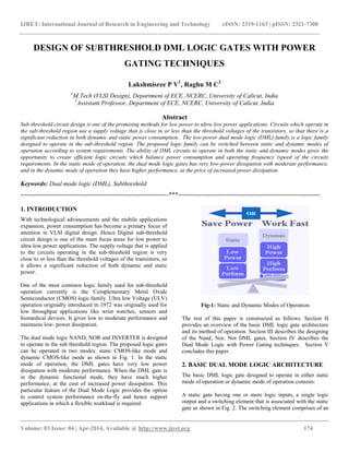
  • 1. IJRET: International Journal of Research in Engineering and Technology eISSN: 2319-1163 | pISSN: 2321-7308 __________________________________________________________________________________________ Volume: 03 Issue: 04 | Apr-2014, Available @ http://www.ijret.org 174 DESIGN OF SUBTHRESHOLD DML LOGIC GATES WITH POWER GATING TECHNIQUES Lakshmisree P V1 , Raghu M C2 1 M.Tech (VLSI Design), Department of ECE, NCERC, University of Calicut, India 2 Assistant Professor, Department of ECE, NCERC, University of Calicut, India Abstract Sub-threshold circuit design is one of the promising methods for low power to ultra-low power applications. Circuits which operate in the sub-threshold region use a supply voltage that is close to or less than the threshold voltages of the transistors, so that there is a significant reduction in both dynamic and static power consumption. The low-power dual mode logic (DML) family is a logic family designed to operate in the sub-threshold region. The proposed logic family can be switched between static and dynamic modes of operation according to system requirements. The ability of DML circuits to operate in both the static and dynamic modes gives the opportunity to create efficient logic circuits which balance power consumption and operating frequency (speed of the circuit) requirements. In the static mode of operation, the dual mode logic gates has very low-power dissipation with moderate performance, and in the dynamic mode of operation they have higher performance, at the price of increased power dissipation Keywords: Dual mode logic (DML), Subthreshold -----------------------------------------------------------------------***-------------------------------------------------------------------- 1. INTRODUCTION With technological advancements and the mobile applications expansion, power consumption has become a primary focus of attention in VLSI digital design. Hence Digital sub-threshold circuit design is one of the main focus areas for low power to ultra-low power applications. The supply voltage that is applied to the circuits operating in the sub-threshold region is very close to or less than the threshold voltages of the transistors, so it allows a significant reduction of both dynamic and static power. One of the most common logic family used for sub-threshold operation currently is the Complementary Metal Oxide Semiconductor (CMOS) logic family. Ultra low Voltage (ULV) operation originally introduced in 1972 was originally used for low throughput applications like wrist watches, sensors and biomedical devices. It gives low to moderate performance and maintains low- power dissipation. The dual mode logic NAND, NOR and INVERTER is designed to operate in the sub threshold region. The proposed logic gates can be operated in two modes: static CMOS-like mode and dynamic CMOS-like mode as shown in Fig. 1. In the static mode of operation, the DML gates have very low power dissipation with moderate performance. When the DML gate is in the dynamic functional mode, they have much higher performance, at the cost of increased power dissipation. This particular feature of the Dual Mode Logic provides the option to control system performance on-the-fly and hence support applications in which a flexible workload is required. Fig-1: Static and Dynamic Modes of Operation The rest of this paper is constructed as follows. Section II provides an overview of the basic DML logic gate architecture and its method of operation. Section III describes the designing of the Nand, Nor, Not DML gates. Section IV describes the Dual Mode Logic with Power Gating techniques. Section V concludes this paper. 2. BASIC DUAL MODE LOGIC ARCHITECTURE The basic DML logic gate designed to operate in either static mode of operation or dynamic mode of operation consists: A static gate having one or more logic inputs, a single logic output and a switching element that is associated with the static gate as shown in Fig. 2. The switching element comprises of an
  • 2. IJRET: International Journal of Research in Engineering and Technology eISSN: 2319-1163 | pISSN: 2321-7308 __________________________________________________________________________________________ Volume: 03 Issue: 04 | Apr-2014, Available @ http://www.ijret.org 175 input that is connected to a constant voltage, and another input for providing a signal used for mode selection, an output that is connected to a logic output of the static gate. The switching element can be configured to operate in either of the two modes by: i) disconnecting the static gate output from both the input that is connected to a constant voltage, and the other input for providing a signal used for mode selection, when the mode selection signal applies a constant voltage to the input used for providing mode selection signal, thereby selecting static mode of operation ii) Connecting the static gate output to both the input that is connected to a constant voltage, and the other input for providing a signal used for mode selection, when the mode selection signal applies a dynamic clock signal to the input used for providing mode selection signal, thereby to select dynamic mode operation. Switching the Dual mode logic gates between the two functional modes, static and dynamic, is performed by applying either a constant voltage or a dynamic clock signal at the mode selection input of the switching element. Fig-2: Basic DML Logic When static functional mode is selected an appropriate constant voltage (high or low as required by static gate topology) is applied to the mode selection input of the switching element. The applied constant voltage causes the switching element to disconnect the static gate output from the constant voltage applied, thus enabling static mode of operation. During dynamic mode of operation, the switching element input a dynamic clock signal which has pre-charge and evaluate phases, which will periodically connect the static gate output to the constant voltage level, thus enabling dynamic mode of operation. In the DML circuit designed, the static gate is a CMOS gate and switching element is implemented by either a PMOS or an NMOS transistor. In order to operate the Dual mode logic gate in the dynamic functional mode, the clock (Clk) signal applied to the switching element has two distinct phases: the precharge and evaluation phases. During the precharge phase, the output of the DML gate is charged to high/low, based on the topology of the DML gate. During the following evaluation phase, the DML gate‟s output is evaluated according to the values at the DML gate inputs. The DML topologies, marked Type A and Type B, are illustrated in Fig. 3. Type A topology has an added p-MOS transistor that precharges the output to a logical “1” during the precharge phase. Type B DML topology has an added n-MOS that precharges the gate output to a logical “0” during the precharge phase. Fig-3: Basic DML Type A topology and Type B topology. Switching the DML gates to operate in CMOS-like static mode of operation is done by either by fixing the global Clock (Clk) signal to logic high for Type A topology or by fixing the global Clk signal to logic low for Type B topology. 3. DML NAND, NOR, INVERTER GATES DESIGN Conventional Nand logic gate design is done using Tanner S- Edit EDA tool and its power and performance are found. Also Dual Mode Logic Nand gate Type A and Type B topologies designed and their power consumption and performance were analyzed for static and dynamic mode of operations. The truth table of the 2-input NAND gate is given in Table 1. Table-1: Truth Table of 2-input NAND A B Q 0 0 1 0 1 1 1 0 1 1 1 0 To design a DML gate, the methodology that is to be followed is to place the precharge transistor in parallel to the stacked transistors of the basic CMOS gate. Then, the evaluation of the logic will be performed with the parallel transistors which will make the evaluation process faster.
  • 3. IJRET: International Journal of Research in Engineering and Technology eISSN: 2319-1163 | pISSN: 2321-7308 __________________________________________________________________________________________ Volume: 03 Issue: 04 | Apr-2014, Available @ http://www.ijret.org 176 Fig-4: Schematic of type A Static nand In the DML Type-A Static NAND topology, the switching element is a pMOS transistor connected parallel to the Pull-up network as shown in Fig. 4. The input to the switching element is a constant high voltage to make it OFF. The only difference when designing DML Type-A Dynamic NAND topology, is that the input to the switching element is a clock signal having pre-charge and evaluate phase for dynamic mode of operation. In the DML Type-B Static NAND topology, the switching element is an NMOS transistor connected parallel to the Pull- down network. The input to the switching element is a constant low voltage to make it OFF. The only difference when designing DML Type-B Dynamic NAND topology shown in Fig. 5 is that the input to the switching element is a clock signal having pre-charge and evaluate phase for dynamic mode of operation. Fig-5: Schematic of type B Dynamic nand Conventional NOR logic gate design is done using Tanner S- Edit EDA tool and its power and performance are found. Also Dual Mode Logic Nand gate Type A and Type B topologies designed and their power consumption and performance were analyzed for static and dynamic mode of operations. The truth table of the 2-input NOR gate is given in Table 2. Table-2: Truth Table of 2-input NOR A B Q 0 0 1 0 1 0 1 0 0 1 1 0 In the DML Type-A Static NOR topology, the switching element is a PMOS transistor connected parallel to the Pull-up network which is a series connection of 2 PMOS transistors as shown in Fig. 6. The input to the switching element is a constant high voltage to make it OFF. The only difference when designing DML Type-A Dynamic NOR topology, is that the input to the switching element is a clock signal having pre- charge and evaluate phase for dynamic mode of operation. Fig-6: Schematic of type A Static nor In the DML Type-B Static NOR topology, the switching element is an NMOS transistor connected parallel to the Pull- down network which is a parallel connection of 2 NMOS transistors. The input to the switching element is a constant low voltage to make it OFF. The only difference when designing DML Type-B Dynamic NOR topology is that the input to the switching element is a clock signal having pre-charge and evaluate phase for dynamic mode of operation as shown in Fig. 7.
  • 4. IJRET: International Journal of Research in Engineering and Technology eISSN: 2319-1163 | pISSN: 2321-7308 __________________________________________________________________________________________ Volume: 03 Issue: 04 | Apr-2014, Available @ http://www.ijret.org 177 Fig-7: Schematic of type B Dynamic nor Conventional inverter gate design is done using Tanner S-Edit EDA tool and its power and performance are found. Also Dual Mode Logic Nand gate Type A and Type B topologies designed and their power consumption and performance were analyzed for static and dynamic mode of operations. The truth table of the NOT gate is given in Table 3. Table-3: Truth Table of NOT A Q 0 1 1 0 In the DML Type-A Static NOT topology, the switching element is a PMOS transistor connected parallel to the Pull-up network as shown in Fig. 8. The input to the switching element is a constant high voltage to make it OFF. The only difference when designing DML Type-A Dynamic NOT topology is that the input to the switching element is a clock signal having pre- charge and evaluate phase for dynamic mode of operation. Fig-8: Schematic of type A Static not In the DML Type-B Static NOT topology, the switching element is an NMOS transistor connected parallel to the Pull- down network. The input to the switching element is a constant low voltage to make it OFF. The only difference when designing DML Type-B Dynamic NOT topology is that the input to the switching element is a clock signal having pre- charge and evaluate phase for dynamic mode of operation as shown in Fig. 9. Fig-9: Schematic of type B Dynamic not 4. DML WITH POWER GATING TECHNIQUES Power Gating is an effective implementation that is used in Low Power Designs. While Clock Gating saves the dynamic power of a circuit, Power Gating saves the leakage power. As the technology moves from micron technology to sub-micron technology, the leakage power dissipation dominates the dynamic power dissipation. Fig-10: Power Gating structure The power gated sleep circuit has two modes of operations: 1. Active mode 2. Sleep mode
  • 5. IJRET: International Journal of Research in Engineering and Technology eISSN: 2319-1163 | pISSN: 2321-7308 __________________________________________________________________________________________ Volume: 03 Issue: 04 | Apr-2014, Available @ http://www.ijret.org 178 In active mode, the sleep Signal SLEEP of the transistor is held at logic' 0 'and SLEEP` at logic „1‟ hence both the sleep transistors remain ON. In this case both transistors offer very low resistance and virtual ground (VGND) node potential is pulled down to the ground potential, making the logic difference between the logic circuitry approximately equal to the supply voltage. In sleep mode, the sleep Signal SLEEP of the transistor is held at logic' 1 'and SLEEP` at logic „0‟ hence both the sleep transistors are turned OFF and the logic part is dis-connected from the supply and ground leading to very less power consumption during sleep mode. Power gating is incorporated in to the DML architecture as shown in Fig. 11. Fig-11: DML gate with Power Gating Different methods of power gating like the sleep method, sleepy stack and dual sleep approaches added to the existing Dual mode logic NAND, NOR, NOT gates. The Sleep method is the basic power gating method. The sleep transistors isolate the logic networks and the sleep transistor technique or the sleep method dramatically reduces leakage power during sleep mode. Fig.12 shows Type A Dynamic Dual Mode Logic Nand with sleep power gating technique. Fig-12: Type A dynamic NAND with Sleep Power Gating Technique The sleepy stack approach merges the sleep and stack approaches. The sleepy stack technique splits the existing transistors into two half Size transistors like the stack approach. The activity of the sleep transistors in the sleepy stack method is same as the activity of the sleep transistors in the sleep method. The sleep transistors are turned on during the active mode and they are turned off during the sleep mode. Fig. 13 shows Conventional NOT gate with Sleepy Stack Power Gating Technique. Fig-13: Conventional NOT gate with Sleepy Stack Power Gating Technique The Dual sleep approach has the advantage of using the two extra pull- up and two extra pull-down transistors in sleep mode either in OFF state or in ON state. In normal mode when S=1 the pull down NMOS transistor is in ON state and in the pull-up network the PMOS sleep transistor is in ON state since S‟=0. During sleep mode state S is forced to 0 and hence the pull- down NMOS transistor is in OFF state and PMOS transistor is in ON state and in the pull-up network, PMOS sleep transistor is OFF while NMOS sleep transistor is ON. So in sleep mode state a PMOS is in series with an NMOS both in pull-up network and pull-down network which reduces the power dissipation. Fig.14 shows Type B Static NOR with Dual Sleep Power Gating Technique Fig-14: Type B Static NOR with Dual Sleep Power Gating Technique
  • 6. IJRET: International Journal of Research in Engineering and Technology eISSN: 2319-1163 | pISSN: 2321-7308 __________________________________________________________________________________________ Volume: 03 Issue: 04 | Apr-2014, Available @ http://www.ijret.org 179 The comparison of the NAND, NOR, NOT Dual mode logic gates in terms of power consumption is shown in Table 4. Table- 4: Comparison between NAND, NOR, NOT DML gates NAND NOR NOT CONVENTIONAL 6.24E-09W 5.11E-09W 3.35E-09W TYPE A STATIC 5.32E-09W 4.91E-09W 2.37E-09W TYPE A DYNAMIC 9.44E-09W 5.54E-09W 1.15E-08W TYPE B STATIC 6.07E-09W 5.08E-09W 3.27E-09W TYPE B DYNAMIC 7.02E-09W 5.15E-09W 3.26E-09W The NAND Dual mode logic gate is compared in terms of power consumption for different power gating techniques like sleep method, sleepy stack method and dual sleep method in Table 5. Table-5: Comparison between NAND DML gates with different power gating techniques NAND SLEEP POWER GATING NAND SLEEPY STACK POWER GATING NAND DUAL SLEEP POWER GATING CONVENTIONAL 1.71E-09W 2.06E- 09W 1.01E-08W TYPE A STATIC 1.36E-09W 7.42E- 10W 7.39E-09W TYPE A DYNAMIC 2.73E-09W 3.29E- 09W 1.34E-08W TYPE B STATIC 1.55E-09W 8.32E- 10W 9.87E-09W TYPE B DYNAMIC 2.13E-09W 8.09E- 09W 1.14E-08W The NOR Dual mode logic gate is compared in terms of power consumption for different power gating techniques in Table 6. Also The NOT Dual mode logic gate is compared in terms of power consumption for different power gating techniques in Table 7. Table-6: Comparison between NOR DML gates with different power gating techniques NOR SLEEP POWER GATING NOR SLEEPY STACK POWER GATING NOR DUAL SLEEP POWER GATING CONVENTIONAL 2.98E-09W 2.24E-09W 2.82E-09W TYPE A STATIC 2.27E-09W 2.18E-09W 1.81E-09W TYPE A DYNAMIC 7.72E-09W 2.45E-08W 5.47E-09W TYPE B STATIC 2.95E-09W 1.78E-09W 1.73E-09W TYPE B DYNAMIC 3.04E-09W 3.17E-09W 2.91E-09W Table- 7: Comparison between NOT DML gates with different power gating techniques NOT SLEEP POWER GATING NOT SLEEPY STACK POWER GATING NOT DUAL SLEEP POWER GATING CONVENTIONAL 1.58E-09W 2.57E-10W 1.65E-09W TYPE A STATIC 5.07E-10W 3.45E-12W 2.00E-10W TYPE A DYNAMIC 5.57E-09W 1.93E-09W 1.75E-09W TYPE B STATIC 1.50E-09W 2.06E-10W 1.56E-09W TYPE B DYNAMIC 1.63E-09W 2.86E-10W 1.96E-09W 5. CONCLUSIONS The result obtained leads to the conclusion that while operating in the dynamic mode, sub threshold DML gates achieve an improvement in speed compared to a standard CMOS, while dissipating more power and in the static mode, a reduction of power dissipation is achieved, at the expense of a decrement in performance. The different methods of power gating applied to the DML logic have reduced the power dissipation further. REFERENCES [1] Asaf Kaizerman, Sagi Fisher, and Alexander Fish, “Subthreshold Dual Mode Logic,” IEEE TRANSACTIONS ON VERY LARGE SCALE INTEGRATION (VLSI) SYSTEMS, VOL. 21, NO. 5, MAY 2013 [2] M. Alioto, “Ultralow power VLSI circuit design demystified and explained: A tutorial,” IEEE Trans. Circuits Syst. I, vol. 59, no. 1, pp.3–29, Jan. 2012. [3] A.P.Chandrakasan, S.Sheng and R.W.Brodersen, “Low-power CMOS digital, “Solid-State Circuits, IEEE Journal of, vol.27, pp.473-484, 2002. [4] D.Bol, R. Ambroise, D. Flandre, and J. D. Legat, “Analysis and minimization of practical energy in 45 nm subthreshold logic circuits,” in Proc. IEEE Int. Conf. Comput. Design, Oct. 2008, pp. 294–300. [5] N,Verma, J. Kwong and A.P. Chandrakasan, "Nanometer MOSFET variation in minimum energy subthreshold circuits," Electron Devices, IEEE Transactions on, vol. 55, pp. 163-174, 2008. [6] H.Soeleman and K. Roy, "Ultra-low power digital subthreshold logic circuits," in Proceedings of the
  • 7. IJRET: International Journal of Research in Engineering and Technology eISSN: 2319-1163 | pISSN: 2321-7308 __________________________________________________________________________________________ Volume: 03 Issue: 04 | Apr-2014, Available @ http://www.ijret.org 180 1999 international symposium on Low power electronics and design, pp. 94-96, 1999. [7] J. Kao, S. Narendra and A. Chandrakasan, "Subthreshold leakage modeling and reduction techniques," in Proceedings of the 2002 IEEE/ACM international conference on Computer-aided design, pp. 141-148, 2002. [8] B. H. Calhoun, A. Wang, and A. Chandrakasan, “Modeling and sizing for minimum energy operation in subthreshold circuits,” IEEE J. Solid-State Circuits, vol. 40, no. 9, pp. 1778–1786, Sep. 2005. [9] D. Markovic, C. C. Wang, L. P. Alarcon, and J. M. Rabaey, “Ultralowpower design in near-threshold region,” Proc. IEEE, vol. 98, no. 2, pp.237–252, Feb. 2010. [10] B. Zhai, S. Hanson, D. Blaauw, and D. Sylvester, “Analysis and mitigation of variability in subthreshold design,” in Proc. Int. Symp. Low Power Electron. Design, Aug. 2005, pp. 20–25. [11] Chhavi Saxena, Member, IEEE, Manisha Pattanaik, Student Member IEEE and R.K. Tiwari, “Enhanced Power Gating Schemes for Low Leakage Low Ground Bounce Noise in Deep Submicron Circuits” [12] R. Bhanuprakash, Manisha Pattanaik, S. S. Rajput and Kaushik Mazumdar, “Analysis and Reduction of Ground Bounce Noise and Leakage Current During Mode Transition of Stacking Power Gating Logic Circuits,” TENCON 2009 [13] http://vlsi-soc.blogspot.in/2012/08/power-gating.html BIOGRAPHIES P. V. Lakshmisree, student, is currently pursuing her M.tech VLSI Design in department of ECE in Nehru College of Research and Engineering, Pampady, Trissur. She has completed B.Tech in Electronics and Communication Engineering in SOE,CUSAT,Cochin. Her research areas are VLSI, Low Power Design. Mr. M. C. Raghu, Assistant Professor, Department of ECE, Nehru College of Research and Engineering, Pampady, Trissur. He has completed ME VLSI Design in KCG college of Technology, Chennai under ANNA University. His research areas are VLSI, Digital IC Design.