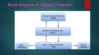
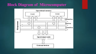
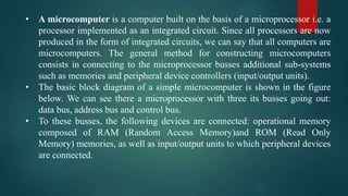
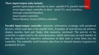
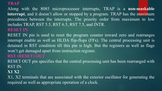
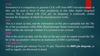
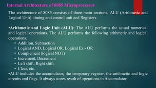
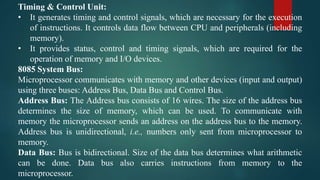
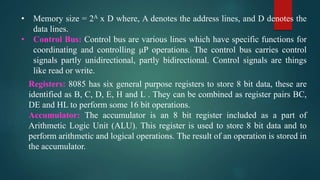
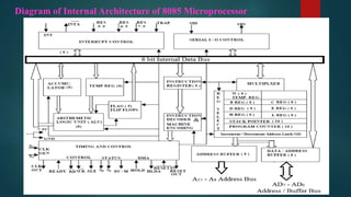
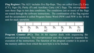
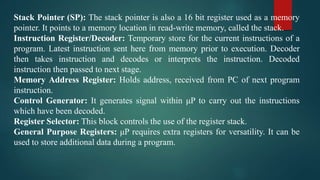
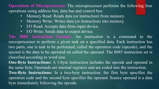
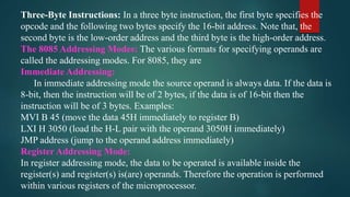
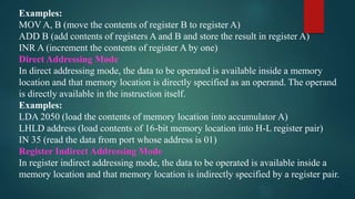
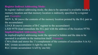
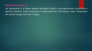
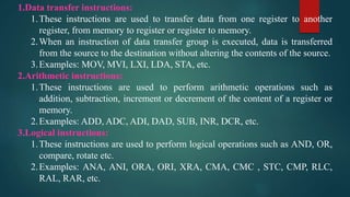
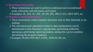
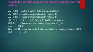
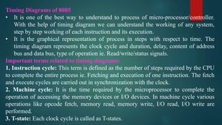
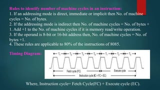
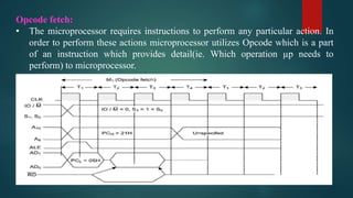
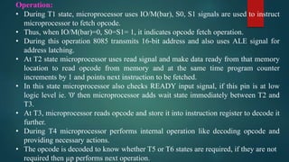
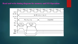
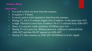
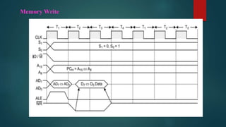
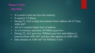
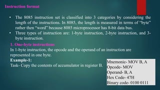
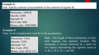
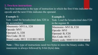
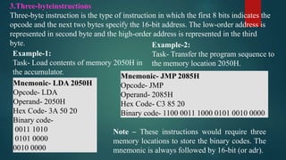
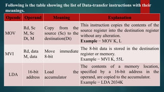
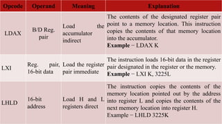
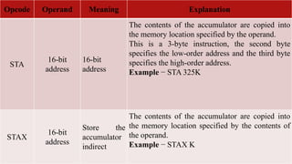
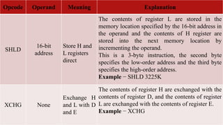
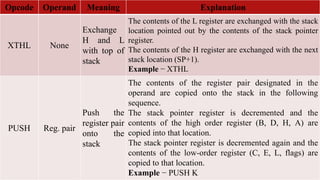
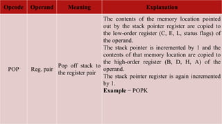
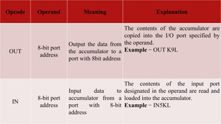
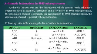
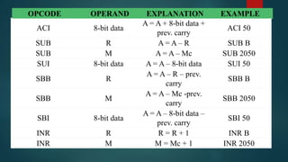
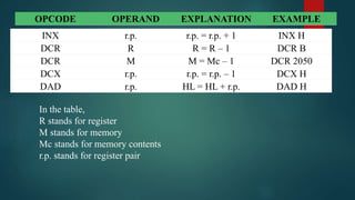
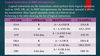
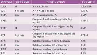
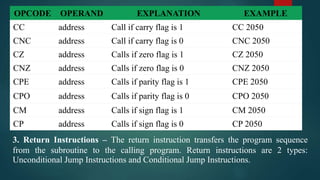
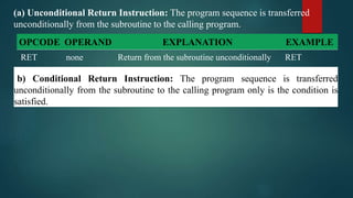
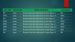
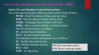
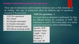
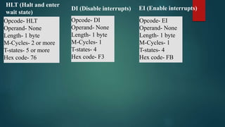
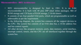
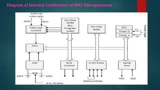
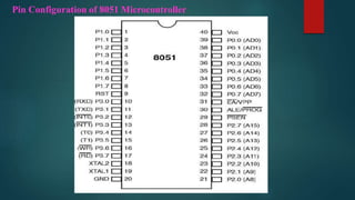
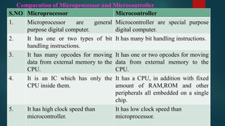
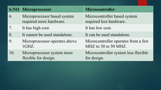
This slides most useful for the Engineering students and Industries peoples. Hence, they are updating the knowledge of microprocessor involved in Mechatronics system.
Over view of Microprocessor 8085 and its applicationiosrjce
Microprocessor is a program controlled semiconductor device (IC), which fetches, decode and
executes instructions. It is versatile in application and is flexible to some extent.
Nowadays, modern microprocessors can perform extremely sophisticated operations in areas such as
meteorology, aviation, nuclear physics and engineering, and take up much less space as well as delivering
superior performance Here is a brief review of microprocessor and its various application
To understand the basic concepts of 8085 microprocessor, microcontroller. The students will also learn about the programming methods and integration of peripherals to the micro-controller.
A Programmable Logic Controller or programmable controller is an industrial computer that has been designed and adapted for the control of manufacturing processes, such as assembly lines, machines, robotic devices, or any activity that requires high reliability, ease of programming, and process fault diagnosis
Computer engineering - overview of microprocessorsEkeedaPvtLtd
Computer engineering is a part of the Engineering and Technology course that deals with software and computers. It integrates different fields of computer and electronic engineering in order to develop computer software and hardware. The computer engineers are trained with both software and hardware related subjects so that they can understand and implement their knowledge in the real world too. The computer engineers have various opportunities when it comes to their career. The advancement in technology and the requirement of various software has paved a glorious path for computer engineers. From big MNCs to small startups, everyone is in need of a computer genius. Computer engineering mainly deals with microcontrollers and processors, circuit designing, designing personal as well as supercomputers, etc. This stream completely focuses on providing knowledge about both software and hardware for students.
MPMC UNIT-1. Microprocessor 8085 pdf Microprocessor and MicrocontrollerRAHUL RANJAN
Diploma in Electrical Engineering MICROPROCESSOR AND MICROCONTROLLER UNIT-1 Full Notes 📝 Microprocessor 8085 State Board Of Technical Education [SBTE] BIHAR
A microcontroller (MCU) is a small computer on a single integrated circuit consisting of a relatively simple central processing unit (CPU) combined with peripheral devices such as memories, I/O devices, and timers.
By some accounts, more than half of all CPUs sold worldwide are microcontrollers
Water scarcity is the lack of fresh water resources to meet the standard water demand. There are two type of water scarcity. One is physical. The other is economic water scarcity.
Courier management system project report.pdfKamal Acharya
It is now-a-days very important for the people to send or receive articles like imported furniture, electronic items, gifts, business goods and the like. People depend vastly on different transport systems which mostly use the manual way of receiving and delivering the articles. There is no way to track the articles till they are received and there is no way to let the customer know what happened in transit, once he booked some articles. In such a situation, we need a system which completely computerizes the cargo activities including time to time tracking of the articles sent. This need is fulfilled by Courier Management System software which is online software for the cargo management people that enables them to receive the goods from a source and send them to a required destination and track their status from time to time.
Final project report on grocery store management system..pdfKamal Acharya
In today’s fast-changing business environment, it’s extremely important to be able to respond to client needs in the most effective and timely manner. If your customers wish to see your business online and have instant access to your products or services.
Online Grocery Store is an e-commerce website, which retails various grocery products. This project allows viewing various products available enables registered users to purchase desired products instantly using Paytm, UPI payment processor (Instant Pay) and also can place order by using Cash on Delivery (Pay Later) option. This project provides an easy access to Administrators and Managers to view orders placed using Pay Later and Instant Pay options.
In order to develop an e-commerce website, a number of Technologies must be studied and understood. These include multi-tiered architecture, server and client-side scripting techniques, implementation technologies, programming language (such as PHP, HTML, CSS, JavaScript) and MySQL relational databases. This is a project with the objective to develop a basic website where a consumer is provided with a shopping cart website and also to know about the technologies used to develop such a website.
This document will discuss each of the underlying technologies to create and implement an e- commerce website.
Saudi Arabia stands as a titan in the global energy landscape, renowned for its abundant oil and gas resources. It's the largest exporter of petroleum and holds some of the world's most significant reserves. Let's delve into the top 10 oil and gas projects shaping Saudi Arabia's energy future in 2024.
Event Management System Vb Net Project Report.pdfKamal Acharya
In present era, the scopes of information technology growing with a very fast .We do not see any are untouched from this industry. The scope of information technology has become wider includes: Business and industry. Household Business, Communication, Education, Entertainment, Science, Medicine, Engineering, Distance Learning, Weather Forecasting. Carrier Searching and so on.
My project named “Event Management System” is software that store and maintained all events coordinated in college. It also helpful to print related reports. My project will help to record the events coordinated by faculties with their Name, Event subject, date & details in an efficient & effective ways.
In my system we have to make a system by which a user can record all events coordinated by a particular faculty. In our proposed system some more featured are added which differs it from the existing system such as security.
About
Indigenized remote control interface card suitable for MAFI system CCR equipment. Compatible for IDM8000 CCR. Backplane mounted serial and TCP/Ethernet communication module for CCR remote access. IDM 8000 CCR remote control on serial and TCP protocol.
• Remote control: Parallel or serial interface.
• Compatible with MAFI CCR system.
• Compatible with IDM8000 CCR.
• Compatible with Backplane mount serial communication.
• Compatible with commercial and Defence aviation CCR system.
• Remote control system for accessing CCR and allied system over serial or TCP.
• Indigenized local Support/presence in India.
• Easy in configuration using DIP switches.
Technical Specifications
Indigenized remote control interface card suitable for MAFI system CCR equipment. Compatible for IDM8000 CCR. Backplane mounted serial and TCP/Ethernet communication module for CCR remote access. IDM 8000 CCR remote control on serial and TCP protocol.
Key Features
Indigenized remote control interface card suitable for MAFI system CCR equipment. Compatible for IDM8000 CCR. Backplane mounted serial and TCP/Ethernet communication module for CCR remote access. IDM 8000 CCR remote control on serial and TCP protocol.
• Remote control: Parallel or serial interface
• Compatible with MAFI CCR system
• Copatiable with IDM8000 CCR
• Compatible with Backplane mount serial communication.
• Compatible with commercial and Defence aviation CCR system.
• Remote control system for accessing CCR and allied system over serial or TCP.
• Indigenized local Support/presence in India.
Application
• Remote control: Parallel or serial interface.
• Compatible with MAFI CCR system.
• Compatible with IDM8000 CCR.
• Compatible with Backplane mount serial communication.
• Compatible with commercial and Defence aviation CCR system.
• Remote control system for accessing CCR and allied system over serial or TCP.
• Indigenized local Support/presence in India.
• Easy in configuration using DIP switches.
Quality defects in TMT Bars, Possible causes and Potential Solutions.PrashantGoswami42
Maintaining high-quality standards in the production of TMT bars is crucial for ensuring structural integrity in construction. Addressing common defects through careful monitoring, standardized processes, and advanced technology can significantly improve the quality of TMT bars. Continuous training and adherence to quality control measures will also play a pivotal role in minimizing these defects.
CFD Simulation of By-pass Flow in a HRSG module by R&R Consult.pptxR&R Consult
CFD analysis is incredibly effective at solving mysteries and improving the performance of complex systems!
Here's a great example: At a large natural gas-fired power plant, where they use waste heat to generate steam and energy, they were puzzled that their boiler wasn't producing as much steam as expected.
R&R and Tetra Engineering Group Inc. were asked to solve the issue with reduced steam production.
An inspection had shown that a significant amount of hot flue gas was bypassing the boiler tubes, where the heat was supposed to be transferred.
R&R Consult conducted a CFD analysis, which revealed that 6.3% of the flue gas was bypassing the boiler tubes without transferring heat. The analysis also showed that the flue gas was instead being directed along the sides of the boiler and between the modules that were supposed to capture the heat. This was the cause of the reduced performance.
Based on our results, Tetra Engineering installed covering plates to reduce the bypass flow. This improved the boiler's performance and increased electricity production.
It is always satisfying when we can help solve complex challenges like this. Do your systems also need a check-up or optimization? Give us a call!
Work done in cooperation with James Malloy and David Moelling from Tetra Engineering.
More examples of our work https://www.r-r-consult.dk/en/cases-en/
Sachpazis:Terzaghi Bearing Capacity Estimation in simple terms with Calculati...Dr.Costas Sachpazis
Terzaghi's soil bearing capacity theory, developed by Karl Terzaghi, is a fundamental principle in geotechnical engineering used to determine the bearing capacity of shallow foundations. This theory provides a method to calculate the ultimate bearing capacity of soil, which is the maximum load per unit area that the soil can support without undergoing shear failure. The Calculation HTML Code included.
Student information management system project report ii.pdfKamal Acharya
Our project explains about the student management. This project mainly explains the various actions related to student details. This project shows some ease in adding, editing and deleting the student details. It also provides a less time consuming process for viewing, adding, editing and deleting the marks of the students.
2. UNIT II MICROPROCESSOR AND
MICROCONTROLLER
Introduction – Architecture of 8085 – Pin
Configuration – Addressing Modes –Instruction set,
Timing diagram of 8085 – Concepts of 8051
microcontroller – Block diagram,
3. Introduction of Microprocessor
• The first question comes in a mind "What is a microprocessor?”. Let
us start with a more familiar term computer. A digital computer is an
electronic machine capable of quickly performing a wide variety of
tasks. They can be used to compile, correlate, sort, merge and store
data as well as perform calculations.
• A digital computer is different from a general purpose calculator in
that it is capable of operating according to the instructions that are
stored within the computer whereas a calculator must be given
instructions on a step by step basis. By the definition a programmable
calculator is a computer.
4. • Historically, digital computers have been categorized according to the size
using the words large, medium, minicomputer and microcomputer.
• In the early years of development, the emphasis was on large and more
powerful computers. Large and medium sized computers were designed to
store complex scientific and engineering problems.
• These computers were accessible and affordable only to large corporations, big
universities and government agencies.
• In the 1960s’ computers were accessible & affordable only to large
corporations, big universities & government agencies, In late 1960s,
minicomputers were available for use in a office, small collage, medium size
business organization, small factory etc.
• As the technology has advanced from SSI to VLSI & SLSI (very large scale
integration & super large scale integration) the face of the computer has
changed. It has now become possible to build the control processing unit
(CPU) with its related timing functions on a single chip known as
microprocessor.
5. • A microprocessor combined with memory and input/output devices forms a
microcomputer. As for as the computing power is concerned the 32- bit
microcomputers are as powerful as traditional mainframe computers.
• The microcomputer is making an impact on every activity of mankind. It is
being used in almost all control applications. For example analytical and
scientific instruments, data communication, character recognition, musical
instruments, household items, defense equipment's, medical equipment's etc.
• Computers communicate and operate in binary numbers 0 and 1 also known as
bits. It is the abbreviation for the term binary digit. The bit size of a
microprocessor refers to the number of bit which can be processed
simultaneously by the arithmetic circuit of the microprocessor.
• A number of bits taken as a group are this manner is called word. For example,
the first commercial microprocessor the Intel 4004 which was introduced in
1971 is a 4-bit machine and is said to process a 4-bit word.
8. • A microcomputer is a computer built on the basis of a microprocessor i.e. a
processor implemented as an integrated circuit. Since all processors are now
produced in the form of integrated circuits, we can say that all computers are
microcomputers. The general method for constructing microcomputers
consists in connecting to the microprocessor busses additional sub-systems
such as memories and peripheral device controllers (input/output units).
• The basic block diagram of a simple microcomputer is shown in the figure
below. We can see there a microprocessor with three its busses going out:
data bus, address bus and control bus.
• To these busses, the following devices are connected: operational memory
composed of RAM (Random Access Memory)and ROM (Read Only
Memory) memories, as well as input/output units to which peripheral devices
are connected.
9. These input/output units include:
parallel input/output controller in short - parallel I/O, parallel interface,
serial input/output controller in short - serial I/O, serial interface,
interrupt controller(handler),
timer/counter controller,
Direct Memory Access (DMA) controller.
Parallel input/output controller maintains information exchange with peripheral
devices, which send data in the parallel form. Examples of such devices are printers,
display monitor, hard and floppy disk memories, keyboard. The activity of the
controller is supervised by the microprocessor, which intervenes on each transfer of
data by execution of respective instructions of data read or write from (to) the
controller. The controller itself transfers data from its internal memory (registers) to
peripheral devices.
10. The serial input/output controller maintains information exchange with
peripheral devices, which send data in the serial form. Examples of such devices
are a mouse and a modem for interconnections through telephone network. The
controller implements in hardware conversion of serial data into their parallel
form and vice versa (with the use of serial/parallel registers). The functioning of
the controller is controlled by the microprocessor, which intervenes on each
termination of data conversion by execution of respective data read or write
instructions.
Interrupt controller provides servicing interrupts coming in parallel from many
external devices. Its task consists in receiving interrupt requests, registering them,
performing selection to choose one which is to be serviced by the processor. The
controller communicates with the processor to enable sending the identifier of the
selected interrupt and to exchange control signals. The interrupt controller is
supervised by the processor, which services the interrupt after receiving the
interrupt from the controller.
11. The DMA controller enables parallel data exchange between external devices
and the operational memory without involvement of the processor. This
controller enables autonomous data transfers to/from operational memory. These
transfers do not engage the processor, which can proceed with computations at
the same time.
12. 8085 Microprocessor
Bit: A bit is a single binary digit.
Word: A word refers to the basic data size or bit size that can be processed by the
arithmetic and logic unit of the processor. A 16-bit binary number is called a word
in a 16-bit processor.
Memory Word: The number of bits that can be stored in a register or memory
element is called a memory word.
Bus: A bus is a group of wires (lines) that carry similar information.
System Bus: The system bus is a group of wires used for communication between
the microprocessor and peripherals. Address Bus: It carries the address, which is a
unique binary pattern used to identify a memory location or an I/O port.
Data Bus: The data bus is used to transfer data between memory and processor or
between I/O device and processor.
Control Bus: The control bus carry control signals, which consists of signals for
selection of memory or I/O device from the given address, direction of data
transfer and synchronization of data transfer in case of slow devices.
13. It is a programmable electronics chip ( Integrated Circuit (IC) ). A single IC has
computing and decision making capabilities similar to central processing unit of a
computer. It is used in almost all types of electronics devices like mobile phones,
printers, washing machines, etc. and also used in advanced applications like
radars, satellites and flights. It has 8 bit data bus and 16 bit address bus, thus it is
capable of addressing 64 KB of memory.
• It has 8 bit ALU 8 bit ALU that can perform 8 bit operations.
• Lower order address bus is multiplexed with data bus to minimize the chip
size.
• The 8085 microprocessor is an 8-bit processor available as a 40-pin IC
package (shown the figure below) and uses +5 V for power. It can run at a
maximum frequency of 3 MHz.
8085 Microprocessor
14. • The 40 pins of the microprocessor can be divided into six groups such as
address bus, data bus, control signals & status signals; power supply &
frequency, externally started signals and serial input/output ports.
16. Address Bus (A8-A15)
The address bus pins are ranges from A8 to A15 and these are mainly
applicable to the most considerable memory address bit.
Address Bus (or) Data Bus (AD0-AD7)
The address bus pins or data bus pins are ranges from AD0 to AD7, and these
pins are applicable for LSB (least significant bits) of the address bus in the
primary apparatus CLK cycle as well as employed as a data bus for second clock
cycle & third clock cycle.
A CLK cycle can be designed as, the time in use among two oscillator’s nearby
pulses, or simply it can refer to zero volts. Here the first clock is the primary
transition of pulse ranges from 0V to 5V & then reaches back to 0V.
Address Latch Enable (ALE)
Basically, ALE assists in de-multiplexing the data bus as well as low order
address. This will go high throughout the primary clock cycle as well as allows the
address bits with low order. The address bus with low order is added for memory
otherwise any exterior latch.
17. Status Signal (IO/M)
The status signal IO/M resolves whether the address is intended for memory or
input/output. When the address is high then the address of the address bus is used
for the devices of input/output devices. When the address is low then the address of
the address bus is used for the memory.
Status Signals (S0-S1)
The status signals S0, S1 gives different functions as well as status based on
their status.
• When the S0, S1 are 01 then the operation will be HALT.
• the S0, S1 is 10 then the operation will be WRITE
• When the S0, S1 is 10 then the operation will be READ
• When the S0, S1 are 11 then the operation will be FETCH
Active Low Signal (RD)
The RD is an energetic low signal and an operation is executed whenever the
indication goes small, and it is used for controlling the microprocessor READ
operation. When RD pin goes small then the 8085 microprocessor understands the
information from I/O device or memory.
18. Active Low Signal (WR)
This is an energetic low signal, and it controls the microprocessor’s write operations.
Whenever WR pin goes small, then the information will be written to the I/O device or
memory.
READY
The READY pin is employed with the 8085 microprocessor for ensuring whether a device
is set for accepting or transferring data. A device may be an A/D converter or LCD
display, etc. These devices are associated with the 8085 microprocessor with the READY-
pin. When this pin is high, the device is prepared for transferring the information, if it is
not then the microprocessor stays until this pin goes high.
HOLD
The HOLD pin specifies when any device is demanding the employ of address as well as a
data bus. The two devices are LCD as well as A/D converter. Assume that if A/D
converter is employing the address bus as well as a data bus. When LCD desires the utilize
of both the buses by providing HOLD signal, subsequently the microprocessor transmits
the control signal toward the LCD after that the existing cycle will be ended. When the
LCD procedure is over, then the control signal is transmitted reverse to A/D converter.
19. HLDA
This is the response signal of HOLD, and it specifies whether this signal is obtained or
not obtained. After the implementation of HOLD demand, this signal will go low.
INTR
This is an interrupt signal, and the priority of this among the interrupts is low. This
signal can be allowed or not allowed by the software. When INTR pin goes high then
the 8085 microprocessor completes the instruction of current which is being executed
and then recognizes the INTR signal and progresses it.
INTA
When the 8085 microprocessor gets an interrupt signal, then it should be recognized.
This will be done by INTA. As a result, when the interrupt will be obtained then INTA
will go high.
RST 5.5, RST 6.5, RST 7.5
These pins are the restart maskable interrupts or Vectored Interrupts, used to insert an
inner restart function repeatedly. All these interrupts are maskable, they can be allowed
or not allowed by using programs.
20. TRAP
Along with the 8085 microprocessor interrupts, TRAP is a non-maskable
interrupt, and it doesn’t allow or stopped by a program. TRAP has the maximum
precedence between the interrupts. The priority order from maximum to low
includes TRAP, RST 5.5, RST 6.5, RST 7.5, and INTR.
RESET IN
RESET IN pin is used to reset the program counter toward zero and rearranges
interrupt enable as well as HLDA flip-flops (FFs). The central processing unit is
detained in RST condition till this pin is high. But the registers as well as flags
won’t get damaged apart from instruction register.
RST (RESET) OUT
RESET OUT pin specifies that the central processing unit has been rearranged with
RST IN.
X1 X2
X1, X2 terminals that are associated with the exterior oscillator for generating the
required as well as appropriate operation of a clock.
21. CLK
Sometimes it is compulsory to generate CLK o/PS from 8085 microprocessors so
they can be used in favor of other peripherals or else other digital integrated
circuits. This is offered with CLK pin. Its frequency is continually similar
because the frequency at which the microprocessor works.
SID
This is a serial i/p data, and the information on this pin is uploaded into the 7th-
bit of the accumulator while RIM (Read Interrupt Mask) instruction is performed.
RIM verifies the interrupt whether it is covered or not covered.
SOD
This is the serial o/p data, and the data on this pin sends its output toward the 7th-
bit of the accumulator whenever an instruction of SIM is performed.
VSS and VCC
VSS is a ground pin whereas Vcc is +5v pin. Therefore the 8085 pin diagram, as
well as signals, are discussed in detail.
22. The architecture of 8085 consists of three main sections, ALU (Arithmetic and
Logical Unit), timing and control unit and Registers.
Internal Architecture of 8085 Microprocessor
•Arithmetic and Logic Unit (ALU): The ALU performs the actual numerical
and logical operations. The ALU performs the following arithmetic and logical
operations.
• Addition, Subtraction
• Logical AND, Logical OR, Logical Ex - OR
• Complement (logical NOT)
• Increment, Decrement
• Left shift, Right shift
• Clear, etc.
•ALU includes the accumulator, the temporary register, the arithmetic and logic
circuits and flags. It always stores result of operations in Accumulator.
23. Timing & Control Unit:
• It generates timing and control signals, which are necessary for the execution
of instructions. It controls data flow between CPU and peripherals (including
memory).
• It provides status, control and timing signals, which are required for the
operation of memory and I/O devices.
8085 System Bus:
Microprocessor communicates with memory and other devices (input and output)
using three buses: Address Bus, Data Bus and Control Bus.
Address Bus: The Address bus consists of 16 wires. The size of the address bus
determines the size of memory, which can be used. To communicate with
memory the microprocessor sends an address on the address bus to the memory.
Address bus is unidirectional, i.e., numbers only sent from microprocessor to
memory.
Data Bus: Bus is bidirectional. Size of the data bus determines what arithmetic
can be done. Data bus also carries instructions from memory to the
microprocessor.
24. • Memory size = 2A x D where, A denotes the address lines, and D denotes the
data lines.
• Control Bus: Control bus are various lines which have specific functions for
coordinating and controlling μP operations. The control bus carries control
signals partly unidirectional, partly bidirectional. Control signals are things
like read or write.
Registers: 8085 has six general purpose registers to store 8 bit data, these are
identified as B, C, D, E, H and L . They can be combined as register pairs BC,
DE and HL to perform some 16 bit operations.
Accumulator: The accumulator is an 8 bit register included as a part of
Arithmetic Logic Unit (ALU). This register is used to store 8 bit data and to
perform arithmetic and logical operations. The result of an operation is stored in
the accumulator.
26. Flag Register: The ALU includes five flip-flops. They are called Zero (Z), Carry
(CY), Sign (S), Parity (P) and Auxiliary Carry (AC) flags. The microprocessor
uses these flags to test data conditions. The conditions (set or reset) of the flags
are tested through the software instructions. The combination of the flag register
and the accumulator is called Program Status Word (PSW) and PSW is the 16-bit
unit for stack operation.
Program Counter (PC): This 16 bit register deals with sequencing the
execution of instruction. The microprocessor uses this register to sequence the
execution of the instructions. The function of the program counter is to point to
the memory address from which the next byte is to be fetched.
27. Stack Pointer (SP): The stack pointer is also a 16 bit register used as a memory
pointer. It points to a memory location in read-write memory, called the stack.
Instruction Register/Decoder: Temporary store for the current instructions of a
program. Latest instruction sent here from memory prior to execution. Decoder
then takes instruction and decodes or interprets the instruction. Decoded
instruction then passed to next stage.
Memory Address Register: Holds address, received from PC of next program
instruction.
Control Generator: It generates signal within μP to carry out the instructions
which have been decoded.
Register Selector: This block controls the use of the register stack.
General Purpose Registers: μP requires extra registers for versatility. It can be
used to store additional data during a program.
28. Operations of Microprocessor: The microprocessor performs the following four
operations using address bus, data bus and control bus:
• Memory Read: Reads data (or instruction) from memory.
• Memory Write: Writes data (or instruction) into memory.
• I/O Read: Accepts data from input device.
• I/O Write: Sends data to output device.
The 8085 Instruction Format: An instruction is a command to the
microprocessor to perform a given task on a specified data. Each instruction has
two parts, one is task to be performed, called the operation code (opcode), and the
second is the data to be operated on called the operand. The 8085 instruction set is
classified according to word size.
One-Byte Instructions: A 1-byte instruction includes the opcode and operand in
the same byte. Operands are internal registers and are coded into the instruction.
Two-Byte Instructions: In a two-byte instruction, the first byte specifies the
operation code and the second byte specifies the operand. Source operand is a data
byte immediately following the opcode.
29. Three-Byte Instructions: In a three byte instruction, the first byte specifies the
opcode and the following two bytes specify the 16-bit address. Note that, the
second byte is the low-order address and the third byte is the high-order address.
The 8085 Addressing Modes: The various formats for specifying operands are
called the addressing modes. For 8085, they are
Immediate Addressing:
In immediate addressing mode the source operand is always data. If the data is
8-bit, then the instruction will be of 2 bytes, if the data is of 16-bit then the
instruction will be of 3 bytes. Examples:
MVI B 45 (move the data 45H immediately to register B)
LXI H 3050 (load the H-L pair with the operand 3050H immediately)
JMP address (jump to the operand address immediately)
Register Addressing Mode:
In register addressing mode, the data to be operated is available inside the
register(s) and register(s) is(are) operands. Therefore the operation is performed
within various registers of the microprocessor.
30. Examples:
MOV A, B (move the contents of register B to register A)
ADD B (add contents of registers A and B and store the result in register A)
INR A (increment the contents of register A by one)
Direct Addressing Mode
In direct addressing mode, the data to be operated is available inside a memory
location and that memory location is directly specified as an operand. The operand
is directly available in the instruction itself.
Examples:
LDA 2050 (load the contents of memory location into accumulator A)
LHLD address (load contents of 16-bit memory location into H-L register pair)
IN 35 (read the data from port whose address is 01)
Register Indirect Addressing Mode
In register indirect addressing mode, the data to be operated is available inside a
memory location and that memory location is indirectly specified by a register pair.
31. Register Indirect Addressing Mode:
In register indirect addressing mode, the data to be operated is available inside a
memory location and that memory location is indirectly specified by a register
pair. Examples
MOV A, M (move the contents of the memory location pointed by the H-L pair to
the accumulator)
LDAX B (move contains of B-C register to the accumulator)
LXIH 9570 (load immediate the H-L pair with the address of the location 9570)
Implied/Implicit Addressing Mode:
In implied/implicit addressing mode the operand is hidden and the data to be
operated is available in the instruction itself. Examples
CMA (finds and stores the 1’s complement of the contains of accumultor A in A)
RRC (rotate accumulator A right by one bit)
RLC (rotate accumulator A left by one bit)
32. 8085 Instruction set
An instruction is a binary pattern designed inside a microprocessor to perform a
specific function. Each instruction is represented by 8 bit binary value. Instruction
set can be categorized into 5 types:
33. 1.Data transfer instructions:
1.These instructions are used to transfer data from one register to another
register, from memory to register or register to memory.
2.When an instruction of data transfer group is executed, data is transferred
from the source to the destination without altering the contents of the source.
3.Examples: MOV, MVI, LXI, LDA, STA, etc.
2.Arithmetic instructions:
1.These instructions are used to perform arithmetic operations such as
addition, subtraction, increment or decrement of the content of a register or
memory.
2.Examples: ADD, ADC, ADI, DAD, SUB, INR, DCR, etc.
3.Logical instructions:
1.These instructions are used to perform logical operations such as AND, OR,
compare, rotate etc.
2.Examples: ANA, ANI, ORA, ORI, XRA, CMA, CMC , STC, CMP, RLC,
RAL, RAR, etc.
34. 4. Branching Instructions:
1.These instructions are used to perform conditional and unconditional
jump, subroutine call and return, and restart.
2.Examples: JZ, JNZ, JC, JNC, JP, JM, JPE, JPO, CALL, RET, RST, etc.
5. Machine Control Instructions:
1.These instructions control machine functions such as Halt, Interrupt, or do
nothing.
2.The microprocessor operations related to data manipulation can be
summarized in four functions: copying data, performing arithmetic
operations, performing logical operations, testing for a given condition
and alerting the program sequence.
3.Example: PUSH, POP, HLT, XTHL, NOP, EI, DI, etc.
35. Example-1: Write 8085 assembly program for multiplying two 8 bit
numbers
MVI A,00 ; Load immediate data into accumulator.
MVI B,02 ; Load immediate data into register B.
MVI C,04 ; Load immediate data into register C.
LOOP: ADD B ; Add the content of to accumulator.
DCR C ; Decrement the content of register C by 1.
JNZ LOOP
STA 1000 H ; Store the content of accumulator to memory location 1000 H
HLT ; Halt
36. Timing Diagrams of 8085
• It is one of the best way to understand to process of micro-processor/controller.
With the help of timing diagram we can understand the working of any system,
step by step working of each instruction and its execution.
• It is the graphical representation of process in steps with respect to time. The
timing diagram represents the clock cycle and duration, delay, content of address
bus and data bus, type of operation ie. Read/write/status signals.
Important terms related to timing diagrams:
1. Instruction cycle: This term is defined as the number of steps required by the CPU
to complete the entire process ie. Fetching and execution of one instruction. The fetch
and execute cycles are carried out in synchronization with the clock.
2. Machine cycle: It is the time required by the microprocessor to complete the
operation of accessing the memory devices or I/O devices. In machine cycle various
operations like opcode fetch, memory read, memory write, I/O read, I/O write are
performed.
3. T-state: Each clock cycle is called as T-states.
37. Rules to identify number of machine cycles in an instruction:
1. If an addressing mode is direct, immediate or implicit then No. of machine
cycles = No. of bytes.
2. If the addressing mode is indirect then No. of machine cycles = No. of bytes +
1. Add +1 to the No. of machine cycles if it is memory read/write operation.
3. If the operand is 8-bit or 16-bit address then, No. of machine cycles = No. of
bytes +1.
4. These rules are applicable to 80% of the instructions of 8085.
Timing Diagram:
Where, Instruction cycle= Fetch Cycle(FC) + Execute cycle (EC).
38. Opcode fetch:
• The microprocessor requires instructions to perform any particular action. In
order to perform these actions microprocessor utilizes Opcode which is a part
of an instruction which provides detail(ie. Which operation µp needs to
perform) to microprocessor.
39. Operation:
• During T1 state, microprocessor uses IO/M(bar), S0, S1 signals are used to instruct
microprocessor to fetch opcode.
• Thus, when IO/M(bar)=0, S0=S1= 1, it indicates opcode fetch operation.
• During this operation 8085 transmits 16-bit address and also uses ALE signal for
address latching.
• At T2 state microprocessor uses read signal and make data ready from that memory
location to read opcode from memory and at the same time program counter
increments by 1 and points next instruction to be fetched.
• In this state microprocessor also checks READY input signal, if this pin is at low
logic level ie. '0' then microprocessor adds wait state immediately between T2 and
T3.
• At T3, microprocessor reads opcode and store it into instruction register to decode it
further.
• During T4 microprocessor performs internal operation like decoding opcode and
providing necessary actions.
• The opcode is decoded to know whether T5 or T6 states are required, if they are not
required then µp performs next operation.
40. Read and write timing diagram for memory and I/O Operation
41. Operation:
• It is used to fetch one byte from the memory.
• It requires 3 T-States.
• It can be used to fetch operand or data from the memory.
• During T1, A8-A15 contains higher byte of address. At the same time ALE
is high. Therefore Lower byte of address A0-A7 is selected from AD0-AD7.
• Since, it is memory ready operation, IO/M(bar) goes low.
• During T2 ALE goes low, RD(bar) goes low. Address is removed from
AD0-AD7 and data D0-D7 appears on AD0-AD7.
• During T3, Data remains on AD0-AD7 till RD(bar) is at low signal.
Memory Read
43. Memory Write
Operation
• It is used to send one byte into memory.
• It requires 3 T-States.
• During T1, ALE is high and contains lower address A0-A7 from
AD0-AD7.
• A8-A15 contains higher byte of address.
• As it is memory operation, IO/M(bar) goes low.
• During T2, ALE goes low, WR(bar) goes low and Address is
removed from AD0-AD7 and then data appears on AD0-AD7.
• Data remains on AD0-AD7 till WR(bar) is low.
45. IO Read:
Operation
• It is used to fetch one byte from an IO port.
• It requires 3 T-States.
• During T1, The Lower Byte of IO address is duplicated
into higher order address bus A8-A15.
• ALE is high and AD0-AD7 contains address of IO
device.
• IO/M (bar) goes high as it is an IO operation.
• During T2, ALE goes low, RD (bar) goes low and data
appears on AD0-AD7 as input from IO device.
• During T3 Data remains on AD0-AD7 till RD(bar) is
low.
47. I/O Write:
Operation
• It is used to writ one byte into IO device.
• It requires 3 T-States.
• During T1, the lower byte of address is duplicated into higher order address
bus A8-A15.
• ALE is high and A0-A7 address is selected from AD0-AD7.
• As it is an IO operation IO/M (bar) goes low.
• During T2, ALE goes low, WR (bar) goes low and data appears on AD0-
AD7 to write data into IO device.
• During T3, Data remains on AD0-AD7 till WR(bar) is low.
48. • The 8085 instruction set is classified into 3 categories by considering the
length of the instructions. In 8085, the length is measured in terms of “byte”
rather then “word” because 8085 microprocessor has 8-bit data bus.
• Three types of instruction are: 1-byte instruction, 2-byte instruction, and 3-
byte instruction.
Instruction format
1. One-byte instructions
In 1-byte instruction, the opcode and the operand of an instruction are
represented in one byte.
Example-1:
Task- Copy the contents of accumulator in register B.
Mnemonic- MOV B, A
Opcode- MOV
Operand- B, A
Hex Code- 47H
Binary code- 0100 0111
49. Example-2:
Task- Add the contents of accumulator to the contents of register B.
Mnemonic- ADD B
Opcode- ADD
Operand- B
Hex Code- 80H
Binary code- 1000 0000
Example-3:
Task- Invert (complement) each bit in the accumulator.
Mnemonic- CMA
Opcode- CMA
Operand- NA
Hex Code- 2FH
Binary code- 0010 1111
Note – The length of these instructions is 8-bit;
each requires one memory location. The
mnemonic is always followed by a letter (or
two letters) representing the registers (such as
A, B, C, D, E, H, L and SP).
50. 2. Two-byte instructions
Two-byte instruction is the type of instruction in which the first 8 bits indicates the
opcode and the next 8 bits indicates the operand.
Example-1:
Task- Load the hexadecimal data 32H in
the accumulator.
Mnemonic- MVI A, 32H
Opcode- MVI
Operand- A, 32H
Hex Code- 3E 32
Binary code- 0011 1110 0011 0010
Example-2:
Task- Load the hexadecimal data F2H
in the register B.
Mnemonic- MVI B, F2H
Opcode- MVI
Operand- B, F2H
Hex Code- 06 F2
Binary code- 0000 0110 1111 0010
Note – This type of instructions need two bytes to store the binary codes. The
mnemonic is always followed by 8-bit (byte) data.
51. 3.Three-byteinstructions
Three-byte instruction is the type of instruction in which the first 8 bits indicates the
opcode and the next two bytes specify the 16-bit address. The low-order address is
represented in second byte and the high-order address is represented in the third
byte.
Example-1:
Task- Load contents of memory 2050H in
the accumulator.
Mnemonic- LDA 2050H
Opcode- LDA
Operand- 2050H
Hex Code- 3A 50 20
Binary code-
0011 1010
0101 0000
0010 0000
Example-2:
Task- Transfer the program sequence to
the memory location 2050H.
Mnemonic- JMP 2085H
Opcode- JMP
Operand- 2085H
Hex Code- C3 85 20
Binary code- 1100 0011 1000 0101 0010 0000
Note – These instructions would require three
memory locations to store the binary codes. The
mnemonic is always followed by 16-bit (or adr).
52. Following is the table showing the list of Data-transfer instructions with their
meanings.
Opcode Operand Meaning Explanation
MOV
Rd, Sc
M, Sc
Dt, M
Copy from the
source (Sc) to the
destination(Dt)
This instruction copies the contents of the
source register into the destination register
without any alteration.
Example − MOV K, L
MVI
Rd, data
M, data
Move immediate
8-bit
The 8-bit data is stored in the destination
register or memory.
Example − MVI K, 55L
LDA
16-bit
address
Load the
accumulator
The contents of a memory location,
specified by a 16-bit address in the
operand, are copied to the accumulator.
Example − LDA 2034K
53. Opcode Operand Meaning Explanation
LDAX
B/D Reg.
pair
Load the
accumulator
indirect
The contents of the designated register pair
point to a memory location. This instruction
copies the contents of that memory location
into the accumulator.
Example − LDAX K
LXI
Reg. pair,
16-bit data
Load the register
pair immediate
The instruction loads 16-bit data in the register
pair designated in the register or the memory.
Example − LXI K, 3225L
LHLD
16-bit
address
Load H and L
registers direct
The instruction copies the contents of the
memory location pointed out by the address
into register L and copies the contents of the
next memory location into register H.
Example − LHLD 3225K
54. Opcode Operand Meaning Explanation
STA
16-bit
address
16-bit
address
The contents of the accumulator are copied into
the memory location specified by the operand.
This is a 3-byte instruction, the second byte
specifies the low-order address and the third byte
specifies the high-order address.
Example − STA 325K
STAX
16-bit
address
Store the
accumulator
indirect
The contents of the accumulator are copied into
the memory location specified by the contents of
the operand.
Example − STAX K
55. Opcode Operand Meaning Explanation
SHLD
16-bit
address
Store H and
L registers
direct
The contents of register L are stored in the
memory location specified by the 16-bit address in
the operand and the contents of H register are
stored into the next memory location by
incrementing the operand.
This is a 3-byte instruction, the second byte
specifies the low-order address and the third byte
specifies the high-order address.
Example − SHLD 3225K
XCHG None
Exchange H
and L with D
and E
The contents of register H are exchanged with the
contents of register D, and the contents of register
L are exchanged with the contents of register E.
Example − XCHG
56. Opcode Operand Meaning Explanation
XTHL None
Exchange
H and L
with top of
stack
The contents of the L register are exchanged with the stack
location pointed out by the contents of the stack pointer
register.
The contents of the H register are exchanged with the next
stack location (SP+1).
Example − XTHL
PUSH Reg. pair
Push the
register pair
onto the
stack
The contents of the register pair designated in the
operand are copied onto the stack in the following
sequence.
The stack pointer register is decremented and the
contents of the high order register (B, D, H, A) are
copied into that location.
The stack pointer register is decremented again and the
contents of the low-order register (C, E, L, flags) are
copied to that location.
Example − PUSH K
57. Opcode Operand Meaning Explanation
POP Reg. pair
Pop off stack to
the register pair
The contents of the memory location pointed
out by the stack pointer register are copied to
the low-order register (C, E, L, status flags) of
the operand.
The stack pointer is incremented by 1 and the
contents of that memory location are copied to
the high-order register (B, D, H, A) of the
operand.
The stack pointer register is again incremented
by 1.
Example − POPK
58. Opcode Operand Meaning Explanation
OUT
8-bit port
address
Output the data from
the accumulator to a
port with 8bit address
The contents of the accumulator are
copied into the I/O port specified by
the operand.
Example − OUT K9L
IN
8-bit port
address
Input data to
accumulator from a
port with 8-bit
address
The contents of the input port
designated in the operand are read and
loaded into the accumulator.
Example − IN5KL
59. Arithmetic instructions in 8085 microprocessor
Arithmetic Instructions are the instructions which perform basic arithmetic
operations such as addition, subtraction and a few more. In 8085 microprocessor,
the destination operand is generally the accumulator. In 8085 microprocessor, the
destination operand is generally the accumulator.
Following is the table showing the list of arithmetic instructions:
OPCODE OPERAND EXPLANATION EXAMPLE
ADD R A = A + R ADD B
ADD M A = A + Mc ADD 2050
ADI 8-bit data A = A + 8-bit data ADI 50
ADC R
A = A + R + prev.
carry
ADC B
ADC M
A = A + Mc + prev.
carry
ADC 2050
60. ACI 8-bit data
A = A + 8-bit data +
prev. carry
ACI 50
SUB R A = A – R SUB B
SUB M A = A – Mc SUB 2050
SUI 8-bit data A = A – 8-bit data SUI 50
SBB R
A = A – R – prev.
carry
SBB B
SBB M
A = A – Mc -prev.
carry
SBB 2050
SBI 8-bit data
A = A – 8-bit data –
prev. carry
SBI 50
INR R R = R + 1 INR B
INR M M = Mc + 1 INR 2050
OPCODE OPERAND EXPLANATION EXAMPLE
61. INX r.p. r.p. = r.p. + 1 INX H
DCR R R = R – 1 DCR B
DCR M M = Mc – 1 DCR 2050
DCX r.p. r.p. = r.p. – 1 DCX H
DAD r.p. HL = HL + r.p. DAD H
In the table,
R stands for register
M stands for memory
Mc stands for memory contents
r.p. stands for register pair
OPCODE OPERAND EXPLANATION EXAMPLE
62. Logical instructions in 8085 microprocessor
Logical instructions are the instructions which perform basic logical operations
such as AND, OR, etc. In 8085 microprocessor, the destination operand is always
the accumulator. Here logical operation works on a bitwise level.
Following is the table showing the list of logical instructions
OPCODE OPERAND DESTINATION EXAMPLE
ANA R A = AAND R ANA B
ANA M A = AAND Mc ANA 2050
ANI 8-bit data
A = AAND 8-bit
data
ANI 50
ORA R A = A OR R ORA B
ORA M A = A OR Mc ORA 2050
ORI 8-bit data
A = A OR 8-bit
data
ORI 50
63. OPCODE OPERAND DESTINATION EXAMPLE
XRA M A = A XOR Mc XRA 2050
XRI 8-bit data A = A XOR 8-bit data XRI 50
CMA none A = 1’s compliment of A CMA
CMP R
Compares R with A and triggers the flag
register
CMP B
CMP M
Compares Mc with A and triggers the flag
register
CMP
CPI 8-bit data
Compares 8-bit data with A and triggers the
flag register
CPI 50
RRC none Rotate accumulator right without carry RRC
RLC none Rotate accumulator left without carry RLC
RAR none Rotate accumulator right with carry RAR
RAL none Rotate accumulator left with carry RAR
64. OPCODE OPERAND DESTINATION EXAMPLE
XRA R A = A XOR R XRA B
CMC none
Compliments the
carry flag
CMC
STC none Sets the carry flag STC
In the table,
R stands for register
M stands for memory
Mc stands for memory contents
65. Branching instructions in 8085 microprocessor
Branching instructions refer to the act of switching execution to a different
instruction sequence as a result of executing a branch instruction.
The three types of branching instructions are:
• Jump (unconditional and conditional)
• Call (unconditional and conditional)
• Return (unconditional and conditional)
1. Jump Instructions – The jump instruction transfers the program sequence to
the memory address given in the operand based on the specified flag. Jump
instructions are 2 types: Unconditional Jump Instructions and Conditional Jump
Instructions.
(a) Unconditional Jump Instructions: Transfers the program sequence to the
described memory address.
66. OPCODE OPERAND EXPLANATION EXAMPLE
JMP address Jumps to the address JMP 2050
(b) Conditional Jump Instructions: Transfers the program sequence to the
described memory address only if the condition in satisfied.
OPCODE OPERAND EXPLANATION EXAMPLE
JC address Jumps to the address if carry flag is 1 JC 2050
JNC address Jumps to the address if carry flag is 0 JNC 2050
JZ address Jumps to the address if zero flag is 1 JZ 2050
JNZ address Jumps to the address if zero flag is 0 JNZ 2050
JPE address Jumps to the address if parity flag is 1 JPE 2050
JPO address Jumps to the address if parity flag is 0 JPO 2050
JM address Jumps to the address if sign flag is 1 JM 2050
JP address Jumps to the address if sign flag 0 JP 2050
67. 2. Call Instructions – The call instruction transfers the program sequence to the
memory address given in the operand. Before transferring, the address of the next
instruction after CALL is pushed onto the stack. Call instructions are 2 types:
Unconditional Call Instructions and Conditional Call Instructions.
(a) Unconditional Call Instructions: It transfers the program sequence to the
memory address given in the operand.
OPCODE OPERAND EXPLANATION EXAMPLE
CALL address Unconditionally calls CALL 2050
(b) Conditional Call Instructions: Only if the condition is satisfied, the
instructions executes.
68. OPCODE OPERAND EXPLANATION EXAMPLE
CC address Call if carry flag is 1 CC 2050
CNC address Call if carry flag is 0 CNC 2050
CZ address Calls if zero flag is 1 CZ 2050
CNZ address Calls if zero flag is 0 CNZ 2050
CPE address Calls if parity flag is 1 CPE 2050
CPO address Calls if parity flag is 0 CPO 2050
CM address Calls if sign flag is 1 CM 2050
CP address Calls if sign flag is 0 CP 2050
3. Return Instructions – The return instruction transfers the program sequence
from the subroutine to the calling program. Return instructions are 2 types:
Unconditional Jump Instructions and Conditional Jump Instructions.
69. (a) Unconditional Return Instruction: The program sequence is transferred
unconditionally from the subroutine to the calling program.
OPCODE OPERAND EXPLANATION EXAMPLE
RET none Return from the subroutine unconditionally RET
(b) Conditional Return Instruction: The program sequence is transferred
unconditionally from the subroutine to the calling program only is the condition is
satisfied.
70. OPCODE OPERAND EXPLANATION EXAMPLE
RC none Return from the subroutine if carry flag is 1 RC
RNC none Return from the subroutine if carry flag is 0 RNC
RZ none Return from the subroutine if zero flag is 1 RZ
RNZ none Return from the subroutine if zero flag is 0 RNZ
RPE none Return from the subroutine if parity flag is 1 RPE
RPO none Return from the subroutine if parity flag is 0 RPO
RM none Returns from the subroutine if sign flag is 1 RM
RP none Returns from the subroutine if sign flag is 0 RP
71. Stack I/O and Machine Control Instructions in 8085 / 8085A
Stack I/O, and Machine Control Instructions:
The following instructions affect the Stack and/or Stack Pointer:
PUSH - Push Two bytes of Data onto the Stack
POP - Pop Two Bytes of Data off the Stack
XTHL - Exchange Top of Stack with H & L
SPHL - Move content of H & L to Stack Pointer
The I/0 instructions are as follows:
IN - Initiate Input Operation
OUT - Initiate Output Operation
The Machine Control instructions are as follows:
EI - Enable Interrupt System
DI - Disable Interrupt System
HLT - Halt
NOP - No Operation
SIM (Set interrupt mask)
RIM (Reset interrupt mask)
72. Machine Control Instructions in Microprocessor
These type of instructions control machine functions such as Halt, Interrupt, or
do nothing. This type of instructions alters the different type of operations
executed in the processor.
1. NOP (No operation)
2. HLT (Halt)
3. DI (Disable interrupts)
4. EI (Enable interrupts)
5. SIM (Set interrupt mask)
6. RIM (Reset interrupt mask) Opcode- NOP
Operand- None
Length- 1 byte
M-Cycles- 1
T-states- 4
Hex code- 00
NOP (No operation) –1
It is used when no operation is performed. No flags
are affected during the execution of NOP. The
instruction is used to fill in time delay or to delete
and insert instructions while troubleshooting.
73. Opcode- HLT
Operand- None
Length- 1 byte
M-Cycles- 2 or more
T-states- 5 or more
Hex code- 76
HLT (Halt and enter
wait state)
DI (Disable interrupts)
Opcode- DI
Operand- None
Length- 1 byte
M-Cycles- 1
T-states- 4
Hex code- F3
EI (Enable interrupts)
Opcode- EI
Operand- None
Length- 1 byte
M-Cycles- 1
T-states- 4
Hex code- FB
74. Microcontrollers - 8051 Architecture
• 8051 microcontroller is designed by Intel in 1981. It is an 8-bit
microcontroller. It is built with 40 pins DIP (dual inline package), 4kb of
ROM storage and 128 bytes of RAM storage, 2 16-bit timers.
• It consists of are four parallel 8-bit ports, which are programmable as well as
addressable as per the requirement.
• In the following diagram, the system bus connects all the support devices to
the CPU. The system bus consists of an 8-bit data bus, a 16-bit address bus
and bus control signals.
• All other devices like program memory, ports, data memory, serial interface,
interrupt control, timers, and the CPU are all interfaced together through the
system bus.
77. Pins 1 to 8 − These pins are known as Port 1. This port doesn’t serve any other
functions. It is internally pulled up, bi-directional I/O port.
Pin 9 − It is a RESET pin, which is used to reset the microcontroller to its initial
values.
Pins 10 to 17 − These pins are known as Port 3. This port serves some functions
like interrupts, timer input, control signals, serial communication signals RxD and
TxD, etc.
Pins 18 & 19 − These pins are used for interfacing an external crystal to get the
system clock.
Pin 20 − This pin provides the power supply to the circuit.
Pins 21 to 28 − These pins are known as Port 2. It serves as I/O port. Higher
order address bus signals are also multiplexed using this port.
78. Pin 29 − This is PSEN pin which stands for Program Store Enable. It is used to
read a signal from the external program memory.
Pin 30 − This is ALE pin which stands for Address Latch Enable. It is used to
demultiplex the address-data signal of port.
Pin 31 − This is EA pin which stands for External Access input. It is used to
enable/disable the external memory interfacing.
Pins 32 to 39 − These pins are known as Port 0. It serves as I/O port. Lower
order address and data bus signals are multiplexed using this port.
Pin 40 − This pin is used to provide power supply to the circuit.
79. Input Configuration
If any pin of this port is configured as an input, then it acts as if it “floats”, i.e.
the input has unlimited input resistance and in-determined potential.
Output Configuration
When the pin is configured as an output, then it acts as an “open drain”. By
applying logic 0 to a port bit, the appropriate pin will be connected to ground
(0V), and applying logic 1, the external output will keep on “floating”.
In order to apply logic 1 (5V) on this output pin, it is necessary to build an
external pullup resistor.
80. S.NO Microprocessor Microcontroller
1. Microprocessor are general
purpose digital computer.
Microcontroller are special purpose
digital computer.
2. It has one or two types of bit
handling instructions.
It has many bit handling instructions.
3. It has many opcodes for moving
data from external memory to the
CPU.
It has one or two opcodes for moving
data from external memory to the
CPU.
4. It is an IC which has only the
CPU inside them.
It has a CPU, in addition with fixed
amount of RAM,ROM and other
peripherals all embedded on a single
chip.
5. It has high clock speed than
microcontroller.
It has low clock speed than
microprocessor.
Comparation of Microprocessor and Microcontroller
81. S.NO Microprocessor Microcontroller
6. Microprocessor based system
required more hardware.
Microcontroller based system
required less hardware.
7. It has high cost. It has low cost.
8. It cannot be used standalone. It can be used standalone.
9. Microprocessor operates above
1GHZ.
Microcontroller operates from a few
MHZ to 30 to 50 MHZ.
10. Microprocessor system more
flexible for design.
Microcontroller system less flexible
for design.