Downloaded 146 times
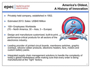
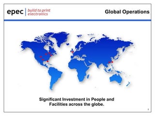
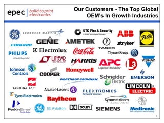


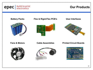

Epec Engineered Technologies, established in 1952, is a leading provider of printed circuit boards and other electronic products, focusing on various high-tech applications including telecommunications, medical, and military sectors. The company emphasizes quality, rapid delivery, and an integrated supply chain, supported by significant investments in technology and facilities worldwide. Epec also offers customized inventory management solutions to meet unique customer requirements and maintains a strong commitment to engineering excellence and production efficiency.


