EMI Shielding Methods for Flex & Rigid-Flex PCB Designs

Critical flex and rigid-flex circuit applications often must pass very stringent electromagnetic (EM) or radio frequency (RF) interference requirements. This type of interference, if absorbed or emitted, can negatively impact the functionality and reliability of the end product when in use. To prevent this from occurring, the circuit design must incorporate shielding to eliminate either the absorption or transmission of EM or RF interference. For flex and rigid-flex PCB designs, there are two types of shielding solutions that can be applied, but which is best suited will depend upon other design requirements. In this webinar, we review shielding methods and how to implement them in a flex or rigid-flex PCB design to ensure interference free operation of your design. For more information on our custom flex and rigid-flex circuit solutions, visit https://www.epectec.com/flex.

Recommended
More Related Content
What's hot
What's hot (20)
Similar to EMI Shielding Methods for Flex & Rigid-Flex PCB Designs
Similar to EMI Shielding Methods for Flex & Rigid-Flex PCB Designs (20)
More from Epec Engineered Technologies
More from Epec Engineered Technologies (19)
Recently uploaded
Recently uploaded (20)
EMI Shielding Methods for Flex & Rigid-Flex PCB Designs
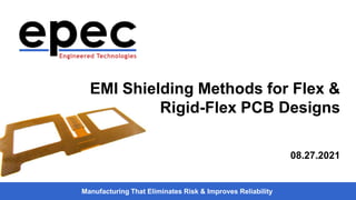
- 1. Manufacturing That Eliminates Risk & Improves Reliability EMI Shielding Methods for Flex & Rigid-Flex PCB Designs 08.27.2021
- 2. Manufacturing That Eliminates Risk & Improves Reliability 2 Agenda EMI Overview Shielding Methods for Flex & Rigid-Flex Designs – Available options: • Copper Layers • Silver Epoxy Ink • Shielding Film Pros & Cons Gerber Design Requirements
- 3. Manufacturing That Eliminates Risk & Improves Reliability 3 Introduction
- 4. Manufacturing That Eliminates Risk & Improves Reliability 4 Introduction EMI definition: – A disturbance generated by an electrical source that affects an electrical circuit by electromagnetic induction, electrostatic coupling, or conduction. Negative impact of EMI: – May degrade the performance of a circuit or even stop it from functioning. – Effects can range from an increase in error rate to a total loss of data. Why shield at the circuit level? – Reduces overall costs when shielded closest to the sensitive circuits.
- 5. Manufacturing That Eliminates Risk & Improves Reliability 5 Shielding Methods
- 6. Manufacturing That Eliminates Risk & Improves Reliability 6 Shielding Methods – Copper Layers Construction: – Additional copper layers added external of signals. – Same solution as used in rigid PCB designs. – Solid plane (preferred) or cross hatched plane layers. Required solution for controlled impedance. Interconnects to ground circuit through via holes. Stitched vias possible but will degrade flexibility. – Vias in flex area not recommended by IPC 2223.
- 7. Manufacturing That Eliminates Risk & Improves Reliability 7 Shielding Methods – Copper Layers (continued)
- 8. Manufacturing That Eliminates Risk & Improves Reliability 8 Shielding Methods – Silver Epoxy Ink Construction: – Layer of silver ink added external of the flex area primary coverlay and encapsulated with secondary coverlay. Connects to ground through selective coverlay openings in primary coverlay and is encapsulated by secondary coverlay. Added costs due to many added process steps and additional materials. – E.g.: silk screening/baking/2nd coverlay (repeat for 2-sided shielding). Old school technology.
- 9. Manufacturing That Eliminates Risk & Improves Reliability 9 Shielding Methods – Silver Epoxy Ink (continued)
- 10. Manufacturing That Eliminates Risk & Improves Reliability 10 Shielding Methods – Shielding Film Specialized film laminated to external coverlays. 3-layer construction: – Electrically conductive adhesive/metallic deposition layer/insulation layer. Shield connects to ground through selective coverlay openings in primary coverlay and is encapsulated by secondary coverlay. Shield layer Insulation layer is friction resistant.
- 11. Manufacturing That Eliminates Risk & Improves Reliability 11 Application: 1 Layer Flex
- 12. Manufacturing That Eliminates Risk & Improves Reliability 12 Application: Multi-Layer Flex
- 13. Manufacturing That Eliminates Risk & Improves Reliability 13 Application: Rigid-Flex
- 14. Manufacturing That Eliminates Risk & Improves Reliability 14 Shielding Method – Pros & Cons
- 15. Manufacturing That Eliminates Risk & Improves Reliability 15 Shielding Method – Copper Layers: Pros Most effective shielding method. Controlled impedance capable. Best for shielding in higher density component areas. Suitable for all flex and rigid-flex designs. Can be extend under flex stiffeners.
- 16. Manufacturing That Eliminates Risk & Improves Reliability 16 Shielding Method – Copper Layers: Cons Negative impact on cost & flexibility. – Flexibility: • Cross hatched planes improves flexibility but degrades shielding. – Cost: • Added process steps and materials due to increased layer count. Limited application to flex circuits of greater than 2 layers depending upon bend requirements. – Increased thickness and reduced bend capability. Consumes additional circuit real estate due to added vias required to access SMT components.
- 17. Manufacturing That Eliminates Risk & Improves Reliability 17 Shielding Method – Silver Ink: Pros Effective shielding method. Less costly than copper layer shields. More flexible than copper layer shields. Can be extended under stiffeners. Can be added, with limitations, to higher layer count designs. Traditional method used for decades.
- 18. Manufacturing That Eliminates Risk & Improves Reliability 18 Shielding Method – Silver Ink: Cons Added process steps and materials. – 1-2 silver ink layers (screening & baking). – 1-2 additional coverlays. Reduced bend capability. – Increased flex thickness. Not recommended for controlled impedance. Not compatible with rigid-flex designs. Very limited application in high density component areas. – Limited by min. web thickness.
- 19. Manufacturing That Eliminates Risk & Improves Reliability 19 Shielding Method – Silver Ink: Cons (continued)
- 20. Manufacturing That Eliminates Risk & Improves Reliability 20 Shielding Method – Shield Films: Pros Very effective shielding. Most cost-effective and flexible solution. Can be used in component areas with some limitations. Suitable for all flex and rigid-flex designs. Most used solution for non-controlled impedance designs.
- 21. Manufacturing That Eliminates Risk & Improves Reliability 21 Shielding Method – Shield Films: Pros (continued) Shield Effect
- 22. Manufacturing That Eliminates Risk & Improves Reliability 22 Shielding Method – Shielding Film: Cons Not recommended for controlled impedance designs. – Increased impedance tolerance. – Difficult to achieve required dielectric thickness. Limited capability in higher density component areas. – Due to min. web thickness requirements. Exposed ground circuit at flex area outline.
- 23. Manufacturing That Eliminates Risk & Improves Reliability 23 Shielding Method – Gerber Design
- 24. Manufacturing That Eliminates Risk & Improves Reliability 24 Gerber Design – Copper Shields Easiest Gerber design solution. – Simple process of adding external ground planes. Supported by all CAD systems. Vias required to rout circuits up SMT components. Via stitching in flex areas (Faraday cage) possible. – Limits flexibility. – Vias in flex areas not recommended by IPC 2223.
- 25. Manufacturing That Eliminates Risk & Improves Reliability 25 Gerber Design – Copper Shields (continued)
- 26. Manufacturing That Eliminates Risk & Improves Reliability 26 Gerber Design – Silver Ink Shields Most complex Gerber design solution. – Not well-supported (if at all) by CAD systems. Shield designed as an additional coverlay: – 0.020” oversize to primary coverlay. – 0.050” min. web thickness. – 0.020” min. setback from part outline.
- 27. Manufacturing That Eliminates Risk & Improves Reliability 27 Gerber Design – Silver Ink Shields Secondary coverlay required. – 0.010” oversize to primary coverlay to encapsulate silver ink. – 0.020” selective access holes to ground shield. Ground Circuits. – min. 0.020” trace width. Most often requirements defined in mechanical and left to manufacturer to design. Not part of CAD database.
- 28. Manufacturing That Eliminates Risk & Improves Reliability 28 Gerber Design – Shielding Film Simple Gerber design solution. Treated as addition coverlay/mechanical layer – 0.010” oversize to coverlay. – Min web thickness = 0.030”. Selective access holes, 0.020”, in coverlay required to ground shield. Shield extended to part outline preferred. Epoxy strain reliefs required for rigid-flex designs. – Seals shield layer to rigid areas.
- 29. Manufacturing That Eliminates Risk & Improves Reliability 29 Gerber Design – Shielding Film Elimination of exposed edge ground requires shield to be postage stamped in place – Size and shape may prevent – Added cost to manufacture and locate shield
- 30. Manufacturing That Eliminates Risk & Improves Reliability 30 Gerber Design – Shielding Film (continued) Cannot be extended under stiffeners – Poor adhesion due to slip properties of Shield insulation layer
- 31. Manufacturing That Eliminates Risk & Improves Reliability 31 Summary EMI shielding of flex circuits or flex areas in rigid-flex is easily accomplished. Most applications have at least 1 if not more available shielding options. Preferred shielding solution dependent upon design requirements. – Flexibility required to meet min. bend requirements. – Controlled impedance. – Flex area layer count. All methods provide sufficient shielding to meet stringent EMI requirements. Most used methods today are copper layers and shield films. Silver ink demand and supply is diminishing.
- 32. Manufacturing That Eliminates Risk & Improves Reliability 32 Our Products Battery Packs Flex & Rigid-Flex PCBs Cable Assemblies Printed Circuit Boards RF Products User Interfaces Flexible Heaters EC Fans & Motors
- 33. Manufacturing That Eliminates Risk & Improves Reliability 33 Free Online Technical Resources Epec’s Blog – https://blog.epectec.com/ – Paul’s Author Page – https://blog.epectec.com/author/paul-tome Design Guides & Ebooks – https://www.epectec.com/guides/ Technical Articles – https://www.epectec.com/articles/ On-Demand Webinars – https://www.epectec.com/webinar/
- 34. Manufacturing That Eliminates Risk & Improves Reliability 34 ITAR – NetVia Group Located in Dallas, TX 26,000 sq ft of manufacturing space 25+ Years PCB Experience Up to 40 Layers Embedded Resistors Heavy & Extreme Copper RF & Microwave PCBs Flex & Rigid Flex
- 35. Manufacturing That Eliminates Risk & Improves Reliability 35 Q&A Questions? – Enter any questions you may have in the control panel – If we don’t have time to get to it, we will reply via email
- 36. Manufacturing That Eliminates Risk & Improves Reliability 36 Thank You Check out our website at www.epectec.com. For more information email sales@epectec.com. Stay Connected with Epec Engineered Technologies Follow us on our social media sites for continuous technical updates and information: