 DELIVERING QUALITY SINCE 1952.
SURFACE FINISHES
Technical Webinar
2
SURFACE FINISHES
 Overview:
The printed circuit board surface finish forms a critical interface between the component
to be assembled and the bare PCB. The surface finish has two essential functions:
– To protect the exposed copper circuitry.
– To provide a solderable surface when assembling (soldering) the components to
the PCB.
Most surface finishes are considered SMOBC (Solder Mask Over Bare Copper).
3
SURFACE FINISHES
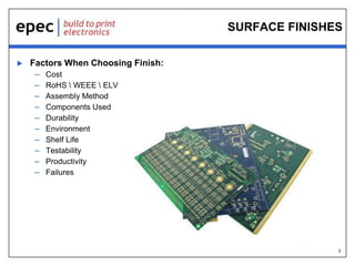
 Factors When Choosing Finish:
– Cost
– RoHS  WEEE  ELV
– Assembly Method
– Components Used
– Durability
– Environment
– Shelf Life
– Testability
– Productivity
– Failures
4
SURFACE FINISHES
 Element Symbols:
Copper Cu
Gold Au
Silver Ag
Tin Sn
Nickel Ni
Lead Pb
Carbon C
Germanium Ge
Palladium Pd
5
SURFACE FINISHES
 Surface Finishes Covered:
– HASL
– Lead Free HASL
– Immersion Tin
– Immersion Silver
– OSP / Entek
– Gold
• ENIG
• Hard Gold
• Wire Bondable Gold
6
SURFACE FINISHES
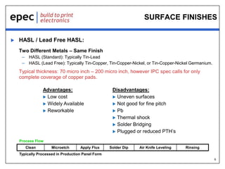
 HASL / Lead Free HASL:
Two Different Metals – Same Finish
– HASL (Standard): Typically Tin-Lead
– HASL (Lead Free): Typically Tin-Copper, Tin-Copper-Nickel, or Tin-Copper-Nickel Germanium.
Typical thickness: 70 micro inch – 200 micro inch, however IPC spec calls for only
complete coverage of copper pads.
Advantages:
 Low cost
 Widely Available
 Reworkable
Disadvantages:
 Uneven surfaces
 Not good for fine pitch
 Pb
 Thermal shock
 Solder Bridging
 Plugged or reduced PTH’s
Process Flow
Clean Microetch Apply Flux Solder Dip Air Knife Leveling Rinsing
Typically Processed in Production Panel Form
7
SURFACE FINISHES
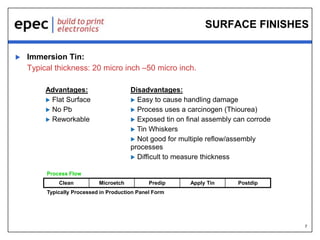
 Immersion Tin:
Typical thickness: 20 micro inch –50 micro inch.
Advantages:
 Flat Surface
 No Pb
 Reworkable
Disadvantages:
 Easy to cause handling damage
 Process uses a carcinogen (Thiourea)
 Exposed tin on final assembly can corrode
 Tin Whiskers
 Not good for multiple reflow/assembly
processes
 Difficult to measure thickness
Process Flow
Clean Microetch Predip Apply Tin Postdip
Typically Processed in Production Panel Form
8
SURFACE FINISHES
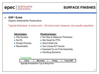
 OSP / Entek
Organic Solderability Preservative
Typical thickness: 4 micro inch – 24 micro inch; however not usually specified.
Advantages:
 Flat Surface
 No Pb
 Simple Process
 Reworkable
Disadvantages:
 No Way to Measure Thickness
 Not Good for PTH
 Short Shelf Life
 Can Cause ICT Issues
 Exposed Cu on Final Assembly
 Handling Sensitive
Process Flow
Clean Microetch Predip Flood OSP
Typically Processed In 1-up or Array Form
9
SURFACE FINISHES
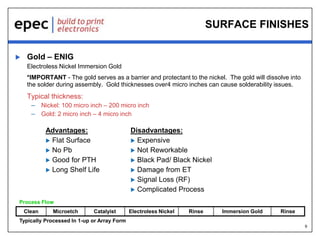
 Gold – ENIG
Electroless Nickel Immersion Gold
*IMPORTANT - The gold serves as a barrier and protectant to the nickel. The gold will dissolve into
the solder during assembly. Gold thicknesses over4 micro inches can cause solderability issues.
Typical thickness:
– Nickel: 100 micro inch – 200 micro inch
– Gold: 2 micro inch – 4 micro inch
Advantages:
 Flat Surface
 No Pb
 Good for PTH
 Long Shelf Life
Disadvantages:
 Expensive
 Not Reworkable
 Black Pad/ Black Nickel
 Damage from ET
 Signal Loss (RF)
 Complicated Process
Process Flow
Clean Microetch Catalyist Electroless Nickel Rinse Immersion Gold Rinse
Typically Processed In 1-up or Array Form
10
SURFACE FINISHES
 Gold – Hard Gold
A.K.A: Flash Gold, Electrolytic Gold, Full body Hard Gold, Tab Gold, Selective Gold
*IMPORTANT - Electrolytic process, all copper surfaces to be plated must be electrically connected
to a rectifier (power supply), unless “gold as etch resist” process is used. Unplated copper must be
covered by mask or resist. Gold has grain stiffeners and brighteners added.
Typical thickness:
– Nickel: 125 micro inch – 150 micro inch
– Gold: 25 micro inch – 40 micro inch
Advantages:
 Hard, Durable Surface
 No Pb
 Long shelf life
Disadvantages:
 Very Expensive
 Extra Processing / Labor Intensive
 Use of Resist / Tape
 Plating / Bus Bars
 Demarcation
 Difficulty with other Surface Finishes
Process Flow
Apply
Resist/Tape
Clean Micoretch
Electroless
Nickel
Rinse
Electrolytic
Gold
Rinse
Strip
Resist/Tape
Clean
Typically Processed in Production Panel Form
11
SURFACE FINISHES
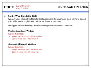
 Gold – Wire Bondable Gold
Typically uses Electrolytic Nickel / Gold processing; however gold must not have added
grain stiffeners or brighteners. Nickel hardness is important.
Two Types of Wire Bonding: Aluminum Wedge and Ultrasonic (Thermal)
Welding Aluminum Wedge:
Typical thickness:
– Nickel: 100 micro inch – 200 micro inch
– Gold: 5 micro inch – 15 micro inch
Ultrasonic (Thermal) Welding:
Typical thickness:
– Nickel: 100 micro inch –200 micro inch
– Gold: 45 micro inch –60 micro inch
12
SURFACE FINISHES
 Summary Matrix
Cost RoHS Typical Thickness Processing
HASL $ No Pad Coverage Panel
Lead Free HASL $ Yes Pad Coverage Panel
Immersion Tin $ Yes 20-50 ui Panel
Immersion Silver $$ Yes 4-12 ui 1-up / Array
OSP/Entek $$ Yes 4-24 ui 1-up / Array
Immersion Gold $$$ Yes
Nickel: 100-200 ui
Gold: 2-4 ui
1-up / Array
Hard Gold $$$$ Yes
Nickel: 125-150 ui
Gold: 25-40 ui
Panel
13
SURFACE FINISHES
For More Information Please Contact
Christopher Perry at 508.995.5171 Ext. 202
cperry@epectec.com
14
Our Products
Battery Packs Flex & Rigid-Flex PCB’s User Interfaces
Fans & Motors Cable Assemblies Printed Circuit Boards
15
The Difference is Quality and Delivery
1. Quicker Delivery - Epec's technology infrastructure and people, including the
Asian and US based operations and engineering teams, enable jobs to get started the
same day the order data is electronically received by our factory.
2. Accurate Information - Epec's on-site personnel provide accurate daily Work
In Process reports so customers can receive immediate order status information, along
with in person verification of all daily reports by Epec staff.
3. Better Quality - Epec ensures higher levels of quality through three key additional
processes. On-site QA inspectors at each facility provide an additional audit before it
leaves Asia, Epec maintains dual UL approval at each facility with quarterly audits, and
perform QA audits at our headquarters in Boston, MA.
4. Flexibility - Each of our manufacturing facilities have been selected for their
best-in-class niche product and delivery solutions, ensuring our optimal facility is
building every order.
16
 If you require additional information please contact us with any
questions or requests.
North American Headquarters
174 Duchaine Blvd.
New Bedford, MA 02745
Tel: (508) 995-5171
Fax: (508) 998-8694
Contact Us By Email:
Sales sales@epectec.com
Quotes quoting@epectec.com
Engineering engineering@epectec.com
Visit Our Website For More Information
www.epectec.com
Stay Connected with Epec Engineered Technologies
Join our Social Community and keep in touch with all our latest technology investments, current news, upcoming
events, and promotions. Visit our Social Media Websites for more information.

Surface Finishes: Why do I need to know more?

  • 1.
     DELIVERING QUALITYSINCE 1952. SURFACE FINISHES Technical Webinar
  • 2.
    2 SURFACE FINISHES  Overview: Theprinted circuit board surface finish forms a critical interface between the component to be assembled and the bare PCB. The surface finish has two essential functions: – To protect the exposed copper circuitry. – To provide a solderable surface when assembling (soldering) the components to the PCB. Most surface finishes are considered SMOBC (Solder Mask Over Bare Copper).
  • 3.
    3 SURFACE FINISHES  FactorsWhen Choosing Finish: – Cost – RoHS WEEE ELV – Assembly Method – Components Used – Durability – Environment – Shelf Life – Testability – Productivity – Failures
  • 4.
    4 SURFACE FINISHES  ElementSymbols: Copper Cu Gold Au Silver Ag Tin Sn Nickel Ni Lead Pb Carbon C Germanium Ge Palladium Pd
  • 5.
    5 SURFACE FINISHES  SurfaceFinishes Covered: – HASL – Lead Free HASL – Immersion Tin – Immersion Silver – OSP / Entek – Gold • ENIG • Hard Gold • Wire Bondable Gold
  • 6.
    6 SURFACE FINISHES  HASL/ Lead Free HASL: Two Different Metals – Same Finish – HASL (Standard): Typically Tin-Lead – HASL (Lead Free): Typically Tin-Copper, Tin-Copper-Nickel, or Tin-Copper-Nickel Germanium. Typical thickness: 70 micro inch – 200 micro inch, however IPC spec calls for only complete coverage of copper pads. Advantages:  Low cost  Widely Available  Reworkable Disadvantages:  Uneven surfaces  Not good for fine pitch  Pb  Thermal shock  Solder Bridging  Plugged or reduced PTH’s Process Flow Clean Microetch Apply Flux Solder Dip Air Knife Leveling Rinsing Typically Processed in Production Panel Form
  • 7.
    7 SURFACE FINISHES  ImmersionTin: Typical thickness: 20 micro inch –50 micro inch. Advantages:  Flat Surface  No Pb  Reworkable Disadvantages:  Easy to cause handling damage  Process uses a carcinogen (Thiourea)  Exposed tin on final assembly can corrode  Tin Whiskers  Not good for multiple reflow/assembly processes  Difficult to measure thickness Process Flow Clean Microetch Predip Apply Tin Postdip Typically Processed in Production Panel Form
  • 8.
    8 SURFACE FINISHES  OSP/ Entek Organic Solderability Preservative Typical thickness: 4 micro inch – 24 micro inch; however not usually specified. Advantages:  Flat Surface  No Pb  Simple Process  Reworkable Disadvantages:  No Way to Measure Thickness  Not Good for PTH  Short Shelf Life  Can Cause ICT Issues  Exposed Cu on Final Assembly  Handling Sensitive Process Flow Clean Microetch Predip Flood OSP Typically Processed In 1-up or Array Form
  • 9.
    9 SURFACE FINISHES  Gold– ENIG Electroless Nickel Immersion Gold *IMPORTANT - The gold serves as a barrier and protectant to the nickel. The gold will dissolve into the solder during assembly. Gold thicknesses over4 micro inches can cause solderability issues. Typical thickness: – Nickel: 100 micro inch – 200 micro inch – Gold: 2 micro inch – 4 micro inch Advantages:  Flat Surface  No Pb  Good for PTH  Long Shelf Life Disadvantages:  Expensive  Not Reworkable  Black Pad/ Black Nickel  Damage from ET  Signal Loss (RF)  Complicated Process Process Flow Clean Microetch Catalyist Electroless Nickel Rinse Immersion Gold Rinse Typically Processed In 1-up or Array Form
  • 10.
    10 SURFACE FINISHES  Gold– Hard Gold A.K.A: Flash Gold, Electrolytic Gold, Full body Hard Gold, Tab Gold, Selective Gold *IMPORTANT - Electrolytic process, all copper surfaces to be plated must be electrically connected to a rectifier (power supply), unless “gold as etch resist” process is used. Unplated copper must be covered by mask or resist. Gold has grain stiffeners and brighteners added. Typical thickness: – Nickel: 125 micro inch – 150 micro inch – Gold: 25 micro inch – 40 micro inch Advantages:  Hard, Durable Surface  No Pb  Long shelf life Disadvantages:  Very Expensive  Extra Processing / Labor Intensive  Use of Resist / Tape  Plating / Bus Bars  Demarcation  Difficulty with other Surface Finishes Process Flow Apply Resist/Tape Clean Micoretch Electroless Nickel Rinse Electrolytic Gold Rinse Strip Resist/Tape Clean Typically Processed in Production Panel Form
  • 11.
    11 SURFACE FINISHES  Gold– Wire Bondable Gold Typically uses Electrolytic Nickel / Gold processing; however gold must not have added grain stiffeners or brighteners. Nickel hardness is important. Two Types of Wire Bonding: Aluminum Wedge and Ultrasonic (Thermal) Welding Aluminum Wedge: Typical thickness: – Nickel: 100 micro inch – 200 micro inch – Gold: 5 micro inch – 15 micro inch Ultrasonic (Thermal) Welding: Typical thickness: – Nickel: 100 micro inch –200 micro inch – Gold: 45 micro inch –60 micro inch
  • 12.
    12 SURFACE FINISHES  SummaryMatrix Cost RoHS Typical Thickness Processing HASL $ No Pad Coverage Panel Lead Free HASL $ Yes Pad Coverage Panel Immersion Tin $ Yes 20-50 ui Panel Immersion Silver $$ Yes 4-12 ui 1-up / Array OSP/Entek $$ Yes 4-24 ui 1-up / Array Immersion Gold $$$ Yes Nickel: 100-200 ui Gold: 2-4 ui 1-up / Array Hard Gold $$$$ Yes Nickel: 125-150 ui Gold: 25-40 ui Panel
  • 13.
    13 SURFACE FINISHES For MoreInformation Please Contact Christopher Perry at 508.995.5171 Ext. 202 cperry@epectec.com
  • 14.
    14 Our Products Battery PacksFlex & Rigid-Flex PCB’s User Interfaces Fans & Motors Cable Assemblies Printed Circuit Boards
  • 15.
    15 The Difference isQuality and Delivery 1. Quicker Delivery - Epec's technology infrastructure and people, including the Asian and US based operations and engineering teams, enable jobs to get started the same day the order data is electronically received by our factory. 2. Accurate Information - Epec's on-site personnel provide accurate daily Work In Process reports so customers can receive immediate order status information, along with in person verification of all daily reports by Epec staff. 3. Better Quality - Epec ensures higher levels of quality through three key additional processes. On-site QA inspectors at each facility provide an additional audit before it leaves Asia, Epec maintains dual UL approval at each facility with quarterly audits, and perform QA audits at our headquarters in Boston, MA. 4. Flexibility - Each of our manufacturing facilities have been selected for their best-in-class niche product and delivery solutions, ensuring our optimal facility is building every order.
  • 16.
    16  If yourequire additional information please contact us with any questions or requests. North American Headquarters 174 Duchaine Blvd. New Bedford, MA 02745 Tel: (508) 995-5171 Fax: (508) 998-8694 Contact Us By Email: Sales sales@epectec.com Quotes quoting@epectec.com Engineering engineering@epectec.com Visit Our Website For More Information www.epectec.com Stay Connected with Epec Engineered Technologies Join our Social Community and keep in touch with all our latest technology investments, current news, upcoming events, and promotions. Visit our Social Media Websites for more information.