SlideShare a Scribd company logo
1 of 4
Download to read offline
Asian Journal of Applied Science and Technology (AJAST)
Volume 1, Issue 2, Pages 36-39, March 2017
© 2017 AJAST All rights reserved. www.ajast.net
Page | 36
Energy Efficient Full Adders for Arithmetic Applications Based on GDI Logic
K.Stella1
, S.Sowmiya2
and V.M.Senthilkumar3
1
PG Student, Department of ECE, Vivekanandha College of Engineering for Women, India. Email: stellakcss@gmail.com
2
PG Student, Department of ECE, Vivekanandha College of Engineering for Women, India. Email: sowmijeyam@gmail.com
3
Associate Professor, Department of ECE, Vivekanandha College of Engineering for Women, India. Email: vmspraneeth@gmail.com
Article Received: 20 February 2017 Article Accepted: 28 February 2017 Article Published: 02 March 2017
1. INTRODUCTION
Adders are extensively used circuit elements in Very Large
Scale Integration (VLSI) systems such as Digital Signal
Processing (DSP) processors, microprocessors etc. It is the
nucleus of many other operations like subtraction,
multiplication, division and parity checkers and addresses
calculation. In most of the digital systems, adders lie in a
critical path which influences the overall system performance.
Hence, enhancing adder‟s performance is becoming an
important goal. The reason behind is that the battery
technology does not advance at the same rate as the
microelectronics technology. There is only a limited amount
of power available for the mobile systems. Therefore, low
power design has become a major design consideration.
The advances in VLSI technology allow hardware realization
of most computing intensive applications such as multimedia
processing, DSP, to enhance the speed of operation.
Moreover, with increasing demand, the researchers are driven
to strive for smaller silicon area, higher speed, longer battery
life and enhanced reliability. The importance of digital
computing lies in full adder design. The design criteria for full
adder are usually multifold. Transistor count, which is one of
the attributes, determines the system complexity of arithmetic
circuits like multiplier, Arithmetic Logic Unit (ALU), etc.
Power consumption and speed would be the other two
important criteria when it comes to the design of full adders.
However, they have a contradictory relationship with each
other.
Therefore, power delay product or energy consumption per
operation has been introduced to accomplish optimal design
tradeoffs. The performance of digital circuits can be
optimized by proper selection of logic styles. Gate Diffusion
Input (GDI) is a lowest power design technique which offers
improved logic swing and less static power dissipation. This
method is suitable for design of fast, low-power circuits, using
a reduced number of transistors. In this paper, an efficient
methodology for digital circuit such as AND, OR, and XOR
gates with full swing is implemented. After that, three full
adders are proposed based on the full swing gates in a
standard 45 nm technology.
2. GDI LOGIC
The basic GDI cell is shown in below Fig.1. GDI logic cell
consists of four terminals. They are:
1) G (Common Gate input of NMOS and PMOS transistor)
2) P (Outer diffusion node of PMOS transistor)
3) N (Outer diffusion node of NMOS transistor)
4) Out (Common diffusion node of both transistors)
Fig.1. GDI basic cell
Table I, shows how a simple change of the input configuration
of the simple GDI cell corresponds to very different Boolean
functions. In this paper, most of the designed circuits were
based on theF1 and F2 functions. The reasons for this are as
follows: 1) Both F1 and F2 are complete logic families. 2) F1
is the only GDI function that can be realized in a standard
p-well CMOS process, because the bulk of any NMOS is
constantly and equally biased. 3) When N input is driven at
ABSTRACT
Addition is a fundamental arithmetic operation and acts as a building block for synthesizing of all other operations. A high-performance adder is one
of the key components in the design of Application Specific Integrated Circuits (ASIC). In this work, three low power full adders are designed with
full swing AND, OR and XOR gates to reduce threshold voltage problem which is commonly encountered in Gate Diffusion Input (GDI) logic. This
problem usually does not allow the full adder circuits to operate without additional inverters. However, the three full adders are successfully realized
using full swing gates with the significant improvement in their performance. The performance of the proposed design is simulated through SPICE
simulations using 45 nm technology models.
Keywords: GDI Logic, Full adder and Full swing.
Asian Journal of Applied Science and Technology (AJAST)
Volume 1, Issue 2, Pages 36-39, March 2017
© 2017 AJAST All rights reserved. www.ajast.net
Page | 37
high logic level and P input is at low logic level, the diodes
between NMOS and PMOS bulks to Out are directly
polarized and there is a short between N and P, resulting in
static power dissipation.
Table I. Various logic functions of GDI cell for different input
configurations
3. PROPOSED FULL ADDERS IN GDI
In this section, three proposed full adder designs featuring
GDI with full swing logic are discussed with the goal to
minimize the circuit complexity and to achieve speed at
cascaded operation. The strategy is to avoid threshold voltage
losses with the help of full swing gates.
3.1. Basic gates for full adder design
The logic function of full adder can be represented as,
Sum= A XOR B XOR Cin (1)
Cout= A AND B + B AND Cin+ A AND Cin (2)
From Eqs. (1) and (2) three basic gates are needed for
implementing the function.
Fig.2. Full swing gates based on F1 and F2 (a) AND (b) OR
and (c) XOR
3.2. Full swing AND, OR and XOR gates using F1 and F2
functions
Conventionally universal gates, namely NAND and NOR can
be used to realize any logical expression. Similarly, in GDI,
two functions are available, namely, F1 (AB) and F2 (A + B)
to realize logical expression. These two functions are also
suffering from a threshold voltage drop. Swing restoration
transistor provided at the output to take care of threshold
voltage loss and the schematic of AND, OR and XOR gates
using F1 and F2 functions are shown in Fig 2. It increases the
transistor count from 2 to 3 for the design of AND and OR yet
the full swing operation can be achieved.
The choice of F1 and F2 for AND and OR gates will be good
since a less number of transistors also provides full swing like
CMOS. However, F1 and F2 based XOR gate implementation
lacks CMOS based design. The reason might be one of the
following:
(i) XOR gate based on F1 and F2 needs a total of 9
transistors, which is twice that of the transistors required for
GDI logic. Therefore, it cuts off the goal of GDI logic, i.e.
function realization using minimal transistor.
(ii) Due to increased transistor count, the overall
input gate capacitance (Cg) of the XOR function increased
since Cg is a direct function of the number of transistor seen
by the inputs.
(iii) The intermediate nodes can be increased
slightly; this might lead to a number of glitches which are the
sources of power consumption.
The realization of AND and OR gates with full swing can be
possible using F1 and F2 functions, respectively, and operate
relatively better than conventional design though not suitable
for XOR realization.
But XOR-XNOR circuits are basic building blocks in various
arithmetic circuits such as adders, multipliers, compressors,
comparators, etc. They provide an intermediate output to
generate the final sum and carry the full adder.
Also the importance of XOR-XNOR functions,
implementations like an adder and multiplier. Therefore, full
swing XOR is necessary to drive successive stages reliably.
3.3. Proposed full swing XOR gate
This subsection details about the proposed XOR gate to
achieve full swing operation. It acts as one of the basic
modules for the realization of three full adder designs and the
performance of the designed adders are investigated under
full swing XOR gate as one of the modules.
The proposed XOR gate uses 4T to provide full swing in the
output. The design of XOR gate using GDI logic without and
with full swing is shown in Fig 3.
The goal is to reduce the circuit complexity and to achieve
faster cascaded operation. The techniques presented in the
literature directly use supply rail VDD for strong „1‟ and VSS
for strong „0‟.
But the proposed design does not use supply rails either GND
or VDD for obtaining the perfect output. It uses input, but only
with proper biasing of a necessary transistor, which may be
either PMOS or NMOS.
N P G Out Function
0 B A A‟B F1
B 1 A A‟+B F2
1 B A A+B OR
B 0 A AB AND
C B A A‟B+AC MUX
0 1 A A‟ NOT
Asian Journal of Applied Science and Technology (AJAST)
Volume 1, Issue 2, Pages 36-39, March 2017
© 2017 AJAST All rights reserved. www.ajast.net
Page | 38
Fig.3. XOR gate (a) using GDI logic and (b) proposed design
For AB = 00, transistor P1 (PMOS), P3 (NMOS) and P4
(PMOS) conduct. The P3 transistor is responsible for
delivering strong „0‟.Likewise, another case when AB = 10,
transistor P2 (NMOS), P3(NMOS) and P4 (PMOS) work for
the given input, in which P4 passes strong „1‟ to the output.
Whereas in other cases, namely AB = 01 and 11, the
transistors P3 and P4 do not change the output potential.
Hence, the correct output for XOR gate is attained with the
proposed design.
4. THREE FULL ADDER DESIGNS
The design of GDI full adder with full swing can be made
possible with the help of full swing gates such as AND, OR
and XOR discussed in the previous section. This design
completely eliminates the swing restoration buffers that
results in improvement in the performance. Three possible
full swing GDI full adders are designed by rewriting the full
adder design expression Eqs. (1) and (2). The full adder‟s
Sum and Cout expressions are given in Eqs. (3) and (4),
respectively.
Sum= Cin (A XOR B) +Cin (A XNOR B) (3)
Cout= (A XOR B)Cin+ (A XOR B)A (4)
Fig.4. Design 1 Full adder
Design 1 uses XOR output as an intermediate result. Sum
output can be attained by multiplexing the XOR and its
inverted version XNOR through Cin input. Cout is obtained by
multiplexing the inputs A and Cin whose output is controlled
by the selection input. The presence of inverter on the critical
path increases the delay of the whole circuit. This design is
simple and requires a total of 18 transistors for realizing the
full adder function.
Design 2 The Sum and Cout expressions are represented in
Eqs. 5 and 6, respectively.
Sum= A XOR B XOR Cin (5)
Cout= Cin (A AND B) + Cin (A OR B) (6)
Fig.5. Design 2 Full adder
Cout function can be realized with the help of AND and OR
gates. AND and OR gates are designed based on F1 and F2,
respectively. Multiplexing the AND and OR operation
through Carry input Cin helps in Cout realization. The XOR
operation on the inputs A, B and Cin achieves Sum function. It
requires total 22 transistors.
Fig.6. Design 3 Full adder
Design 3 It is designed by considering the XOR, AND and
OR gates and the Sum and Cout design expressions are given in
Eqs. (7) and (8).
Sum= A XOR B XOR Cin (7)
Cout= A AND B + (A XOR B) Cin (8)
Asian Journal of Applied Science and Technology (AJAST)
Volume 1, Issue 2, Pages 36-39, March 2017
© 2017 AJAST All rights reserved. www.ajast.net
Page | 39
Sum output can be achieved by XORing the inputs A, Band
Cin. The output Cout is obtained with the help of AND and OR
followed by XOR gate. The realization of AND and OR gate
can be done with the help of full swing F1 and F2 gates.
The GDI based F1 and F2 enables the implementation of
AND and OR with only 3 transistors whereas CMOS needs 6
transistors for achieving the same. The intermediate XOR
gate output is used for computing Cout output. So totally, 23
transistors are needed for designing a full adder. The
proposed full adder based on Design 1, Design 2 and Design 3
are shown in the above Fig 4, 5, 6.
5. RESULT ANALYSIS
Table II. Comparison of Full adders
(a) Design 1 is a best possible candidate for the applications in
which minimum transistor count and low power is a design
requirement.
(b) The Design 2 offers minimum delay, so it can be suitable
for battery operated and real-time applications. It has slightly
increased in transistor count compared with Design 1.
(c) Design 3 lies midway between Design 1 and Design 2, and
offers lower delay than Design 1.
From the obtained results, it can be concluded that all three
designs operate with less energy consumption than existing
adders taken for comparison. Hence, these designs can be
suitable for realizing energy efficient arithmetic applications.
6. CONCLUSION
In this work, three full adder designs that use as few as twenty
transistors per bit are proposed. The design adopts full swing
XOR, AND and OR gates to alleviate the threshold voltage
problem and to enhance the driving capability for cascaded
operation. The enhanced driving capability also facilitates
lower voltage and faster operation which leads to power
consumption. The proposed designs are simulated using the
SPICE simulation tool at 45 nm technology. The comparison
is done in terms of power consumption, propagation delay,
and transistor count.
REFERENCES
[1] A.M. Shams, A.K Darwish and M.A. Bayoumi,
“Performance analysis of low power 1-bit CMOS full adder
cells”, IEEE Trans. VLSI Syst., Vol.10, No.1, pp. 20–29,
2002.
[2] V. Foroutan, M. Taheri , K. Navi and A. Mazreah,
“Design of two low power full adder cells using GDI structure
and hybrid CMOS logic style”, Integration (Amst), Vol.47,
No.1, pp.48–61,2014.
[3] A. Morgenshtein, A. Fish And I.A. Wagner, “Gate
Diffusion Input (GDI)-A power efficient method for digital
combinatorial circuits”, IEEE Trans. VLSI Syst., Vol.10,
No.5, pp.566–581, 2002.
[4] R. Uma and P. Dhavachelvan, “Modified gate diffusion
input technique: a new technique for enhancing performance
in full adder circuits”, Proc. ICCCS, pp.74–81, 2012.
[5] A. Morgenshtein , I. Shwartz and A. Fish, “Full swing
Gate Diffusion Input (GDI) logic case study for low power
CLA adder design”, Integration (Amst), Vol.47, No.1,
pp.62-70, 2014.
[6] M. Aguirre-Hernandez and M. Linares-Aranda, “CMOS
full adders for energy efficient arithmetic applications”, IEEE
Trans. VLSI Syst., Vol.19, No.4, pp. 718–72, 2011.
[7] I. Hassoune, D. Flandre, I. O‟Connor and J. Legat,
“ULPFA: a new efficient design of a power-aware full adder”,
IEEE Trans. Circuits Syst., Vol.57, No.8, pp.2066–2074,
2010.
[8] P. M. Lee, C. H Hsu., Y. H. Hung, “Novel 10-T full adders
realized by GDI structure”, Proc. IEEE Int. Symp. Integr.
Circuits, pp.115–118, 2007.
[9] M. Maeen, V. Foroutan and K. Navi, “On the design of
low power 1 –bit full adder cell”, IEICE Electron. Expert.
Vol.6, No.16, pp.1148–1154, 2009.
[10] R. Patel H. Parasar and M. Wajid, “Faster arithmetic and
logical unit CMOS design with reduced number of
transistors”, Proc. of Intl. Conf. on Advances in
Communication, Network and Computing, Vol.142,
pp.519–522, 2011.
[11] S. Purohit and M. Margala, “Investigating the impact of
logic and implementation for full adder performance”, IEEE
Trans. VLSI Syst., Vol.20, No.7, pp.1327–1331, 2012.
[12] G. Ramana Murthy, C. Senthil Pari, P. Velraj Kumar and
T.S. Lim, “A new 6-T multiplexer based full adder for low
power and leakage current optimization”, IEICE Electronics
Express, Vol.9, No.17, pp.1434–1441, 2012.
[13] R. Singh and S. Akashe, “Modeling and analysis of low
power 10T full adder with reduced ground noise”, J. Circuits
Syst. Comput., Vol.23, No.14, pp.1–14, 2014.

More Related Content

What's hot

Design of 8-Bit Comparator Using 45nm CMOS Technology
Design of 8-Bit Comparator Using 45nm CMOS TechnologyDesign of 8-Bit Comparator Using 45nm CMOS Technology
Design of 8-Bit Comparator Using 45nm CMOS TechnologyIJMER
 
FPGA Implementation of SubByte & Inverse SubByte for AES Algorithm
FPGA Implementation of SubByte & Inverse SubByte for AES AlgorithmFPGA Implementation of SubByte & Inverse SubByte for AES Algorithm
FPGA Implementation of SubByte & Inverse SubByte for AES Algorithmijsrd.com
 
Design of Power Efficient 4x4 Multiplier Based On Various Power Optimizing Te...
Design of Power Efficient 4x4 Multiplier Based On Various Power Optimizing Te...Design of Power Efficient 4x4 Multiplier Based On Various Power Optimizing Te...
Design of Power Efficient 4x4 Multiplier Based On Various Power Optimizing Te...Associate Professor in VSB Coimbatore
 
Performance Analysis of Reversible 16 Bit ALU based on Novel Programmable Rev...
Performance Analysis of Reversible 16 Bit ALU based on Novel Programmable Rev...Performance Analysis of Reversible 16 Bit ALU based on Novel Programmable Rev...
Performance Analysis of Reversible 16 Bit ALU based on Novel Programmable Rev...IRJET Journal
 
Layout Design Analysis of CMOS Comparator using 180nm Technology
Layout Design Analysis of CMOS Comparator using 180nm TechnologyLayout Design Analysis of CMOS Comparator using 180nm Technology
Layout Design Analysis of CMOS Comparator using 180nm TechnologyIJEEE
 
Design of Digital Adder Using Reversible Logic
Design of Digital Adder Using Reversible LogicDesign of Digital Adder Using Reversible Logic
Design of Digital Adder Using Reversible LogicIJERA Editor
 
Hybrid memristor-CMOS implementation of logic gates design using LTSpice
Hybrid memristor-CMOS implementation of logic gates design using LTSpice Hybrid memristor-CMOS implementation of logic gates design using LTSpice
Hybrid memristor-CMOS implementation of logic gates design using LTSpice IJECEIAES
 
Implementation and Comparison of Efficient 16-Bit SQRT CSLA Using Parity Pres...
Implementation and Comparison of Efficient 16-Bit SQRT CSLA Using Parity Pres...Implementation and Comparison of Efficient 16-Bit SQRT CSLA Using Parity Pres...
Implementation and Comparison of Efficient 16-Bit SQRT CSLA Using Parity Pres...IJERA Editor
 
Design and minimization of reversible programmable logic arrays and its reali...
Design and minimization of reversible programmable logic arrays and its reali...Design and minimization of reversible programmable logic arrays and its reali...
Design and minimization of reversible programmable logic arrays and its reali...Sajib Mitra
 
Presentation energy efficient code converters using reversible logic gates
Presentation energy efficient code converters using reversible logic gatesPresentation energy efficient code converters using reversible logic gates
Presentation energy efficient code converters using reversible logic gatesAdityakumar2208
 
Feasible methodology for
Feasible methodology forFeasible methodology for
Feasible methodology forVLSICS Design
 
High Speed Time Efficient Reversible ALU Based Logic Gate Structure on Vertex...
High Speed Time Efficient Reversible ALU Based Logic Gate Structure on Vertex...High Speed Time Efficient Reversible ALU Based Logic Gate Structure on Vertex...
High Speed Time Efficient Reversible ALU Based Logic Gate Structure on Vertex...IJERD Editor
 
Ieee project reversible logic gates by_amit
Ieee project reversible logic gates  by_amitIeee project reversible logic gates  by_amit
Ieee project reversible logic gates by_amitAmith Bhonsle
 
A low power adder using reversible logic gates
A low power adder using reversible logic gatesA low power adder using reversible logic gates
A low power adder using reversible logic gateseSAT Publishing House
 
Implementation of Reversable Logic Based Design using Submicron Technology
Implementation of Reversable Logic Based Design using Submicron TechnologyImplementation of Reversable Logic Based Design using Submicron Technology
Implementation of Reversable Logic Based Design using Submicron TechnologySai Viswanath
 
Delay Optimization of Low Power Reversible Gate using MOS Transistor Level de...
Delay Optimization of Low Power Reversible Gate using MOS Transistor Level de...Delay Optimization of Low Power Reversible Gate using MOS Transistor Level de...
Delay Optimization of Low Power Reversible Gate using MOS Transistor Level de...IJERA Editor
 
An efficient model for design of 64-bit High Speed Parallel Prefix VLSI adder
An efficient model for design of 64-bit High Speed Parallel Prefix VLSI adderAn efficient model for design of 64-bit High Speed Parallel Prefix VLSI adder
An efficient model for design of 64-bit High Speed Parallel Prefix VLSI adderIJMER
 
Power and Delay Analysis of Logic Circuits Using Reversible Gates
Power and Delay Analysis of Logic Circuits Using Reversible GatesPower and Delay Analysis of Logic Circuits Using Reversible Gates
Power and Delay Analysis of Logic Circuits Using Reversible GatesRSIS International
 
FPGA Implementation of Mix and Inverse Mix Column for AES Algorithm
FPGA Implementation of Mix and Inverse Mix Column for AES AlgorithmFPGA Implementation of Mix and Inverse Mix Column for AES Algorithm
FPGA Implementation of Mix and Inverse Mix Column for AES Algorithmijsrd.com
 

What's hot (20)

Design of 8-Bit Comparator Using 45nm CMOS Technology
Design of 8-Bit Comparator Using 45nm CMOS TechnologyDesign of 8-Bit Comparator Using 45nm CMOS Technology
Design of 8-Bit Comparator Using 45nm CMOS Technology
 
FPGA Implementation of SubByte & Inverse SubByte for AES Algorithm
FPGA Implementation of SubByte & Inverse SubByte for AES AlgorithmFPGA Implementation of SubByte & Inverse SubByte for AES Algorithm
FPGA Implementation of SubByte & Inverse SubByte for AES Algorithm
 
Design of Power Efficient 4x4 Multiplier Based On Various Power Optimizing Te...
Design of Power Efficient 4x4 Multiplier Based On Various Power Optimizing Te...Design of Power Efficient 4x4 Multiplier Based On Various Power Optimizing Te...
Design of Power Efficient 4x4 Multiplier Based On Various Power Optimizing Te...
 
Performance Analysis of Reversible 16 Bit ALU based on Novel Programmable Rev...
Performance Analysis of Reversible 16 Bit ALU based on Novel Programmable Rev...Performance Analysis of Reversible 16 Bit ALU based on Novel Programmable Rev...
Performance Analysis of Reversible 16 Bit ALU based on Novel Programmable Rev...
 
Layout Design Analysis of CMOS Comparator using 180nm Technology
Layout Design Analysis of CMOS Comparator using 180nm TechnologyLayout Design Analysis of CMOS Comparator using 180nm Technology
Layout Design Analysis of CMOS Comparator using 180nm Technology
 
Design of Digital Adder Using Reversible Logic
Design of Digital Adder Using Reversible LogicDesign of Digital Adder Using Reversible Logic
Design of Digital Adder Using Reversible Logic
 
Hybrid memristor-CMOS implementation of logic gates design using LTSpice
Hybrid memristor-CMOS implementation of logic gates design using LTSpice Hybrid memristor-CMOS implementation of logic gates design using LTSpice
Hybrid memristor-CMOS implementation of logic gates design using LTSpice
 
Implementation and Comparison of Efficient 16-Bit SQRT CSLA Using Parity Pres...
Implementation and Comparison of Efficient 16-Bit SQRT CSLA Using Parity Pres...Implementation and Comparison of Efficient 16-Bit SQRT CSLA Using Parity Pres...
Implementation and Comparison of Efficient 16-Bit SQRT CSLA Using Parity Pres...
 
Design and minimization of reversible programmable logic arrays and its reali...
Design and minimization of reversible programmable logic arrays and its reali...Design and minimization of reversible programmable logic arrays and its reali...
Design and minimization of reversible programmable logic arrays and its reali...
 
Presentation energy efficient code converters using reversible logic gates
Presentation energy efficient code converters using reversible logic gatesPresentation energy efficient code converters using reversible logic gates
Presentation energy efficient code converters using reversible logic gates
 
Ramya Project
Ramya ProjectRamya Project
Ramya Project
 
Feasible methodology for
Feasible methodology forFeasible methodology for
Feasible methodology for
 
High Speed Time Efficient Reversible ALU Based Logic Gate Structure on Vertex...
High Speed Time Efficient Reversible ALU Based Logic Gate Structure on Vertex...High Speed Time Efficient Reversible ALU Based Logic Gate Structure on Vertex...
High Speed Time Efficient Reversible ALU Based Logic Gate Structure on Vertex...
 
Ieee project reversible logic gates by_amit
Ieee project reversible logic gates  by_amitIeee project reversible logic gates  by_amit
Ieee project reversible logic gates by_amit
 
A low power adder using reversible logic gates
A low power adder using reversible logic gatesA low power adder using reversible logic gates
A low power adder using reversible logic gates
 
Implementation of Reversable Logic Based Design using Submicron Technology
Implementation of Reversable Logic Based Design using Submicron TechnologyImplementation of Reversable Logic Based Design using Submicron Technology
Implementation of Reversable Logic Based Design using Submicron Technology
 
Delay Optimization of Low Power Reversible Gate using MOS Transistor Level de...
Delay Optimization of Low Power Reversible Gate using MOS Transistor Level de...Delay Optimization of Low Power Reversible Gate using MOS Transistor Level de...
Delay Optimization of Low Power Reversible Gate using MOS Transistor Level de...
 
An efficient model for design of 64-bit High Speed Parallel Prefix VLSI adder
An efficient model for design of 64-bit High Speed Parallel Prefix VLSI adderAn efficient model for design of 64-bit High Speed Parallel Prefix VLSI adder
An efficient model for design of 64-bit High Speed Parallel Prefix VLSI adder
 
Power and Delay Analysis of Logic Circuits Using Reversible Gates
Power and Delay Analysis of Logic Circuits Using Reversible GatesPower and Delay Analysis of Logic Circuits Using Reversible Gates
Power and Delay Analysis of Logic Circuits Using Reversible Gates
 
FPGA Implementation of Mix and Inverse Mix Column for AES Algorithm
FPGA Implementation of Mix and Inverse Mix Column for AES AlgorithmFPGA Implementation of Mix and Inverse Mix Column for AES Algorithm
FPGA Implementation of Mix and Inverse Mix Column for AES Algorithm
 

Viewers also liked

Design and Analysis of Low Power High Speed Hybrid logic 8-T Full Adder Circuit
Design and Analysis of Low Power High Speed Hybrid logic 8-T Full Adder CircuitDesign and Analysis of Low Power High Speed Hybrid logic 8-T Full Adder Circuit
Design and Analysis of Low Power High Speed Hybrid logic 8-T Full Adder CircuitAssociate Professor in VSB Coimbatore
 
Real Time ECG and Saline Level Monitoring System Using Arduino UNO Processor
Real Time ECG and Saline Level Monitoring System Using Arduino UNO ProcessorReal Time ECG and Saline Level Monitoring System Using Arduino UNO Processor
Real Time ECG and Saline Level Monitoring System Using Arduino UNO ProcessorAssociate Professor in VSB Coimbatore
 
Tele-Robotic Surgical Arm System with Efficient Tactile Sensors in the Manipu...
Tele-Robotic Surgical Arm System with Efficient Tactile Sensors in the Manipu...Tele-Robotic Surgical Arm System with Efficient Tactile Sensors in the Manipu...
Tele-Robotic Surgical Arm System with Efficient Tactile Sensors in the Manipu...Associate Professor in VSB Coimbatore
 
Real-Time Monitoring and Assessment of Circuit Breaker Operations for Diagnos...
Real-Time Monitoring and Assessment of Circuit Breaker Operations for Diagnos...Real-Time Monitoring and Assessment of Circuit Breaker Operations for Diagnos...
Real-Time Monitoring and Assessment of Circuit Breaker Operations for Diagnos...Associate Professor in VSB Coimbatore
 
Design of a High Directive Gain Reconfigurable Circular Patch Antenna
Design of a High Directive Gain Reconfigurable Circular Patch AntennaDesign of a High Directive Gain Reconfigurable Circular Patch Antenna
Design of a High Directive Gain Reconfigurable Circular Patch AntennaAssociate Professor in VSB Coimbatore
 
Implementation of High Performance Carry Save Adder Using Domino Logic
Implementation of High Performance Carry Save Adder Using Domino LogicImplementation of High Performance Carry Save Adder Using Domino Logic
Implementation of High Performance Carry Save Adder Using Domino LogicAssociate Professor in VSB Coimbatore
 
An Efficient Low Power Convolutional Coding with Viterbi Decoding using FSM
An Efficient Low Power Convolutional Coding with Viterbi Decoding using FSMAn Efficient Low Power Convolutional Coding with Viterbi Decoding using FSM
An Efficient Low Power Convolutional Coding with Viterbi Decoding using FSMAssociate Professor in VSB Coimbatore
 
Design of Three-Input XOR/XNOR using Systematic Cell Design Methodology
Design of Three-Input XOR/XNOR using Systematic Cell Design MethodologyDesign of Three-Input XOR/XNOR using Systematic Cell Design Methodology
Design of Three-Input XOR/XNOR using Systematic Cell Design MethodologyAssociate Professor in VSB Coimbatore
 
Artificial Bee Colony algorithm for Localization in Wireless Sensor Networks
Artificial Bee Colony algorithm for Localization in Wireless Sensor NetworksArtificial Bee Colony algorithm for Localization in Wireless Sensor Networks
Artificial Bee Colony algorithm for Localization in Wireless Sensor NetworksAssociate Professor in VSB Coimbatore
 
Vesceral Control on Electric Gadgets by Smartphones for Smart Abode Environment
Vesceral Control on Electric Gadgets by Smartphones for Smart Abode EnvironmentVesceral Control on Electric Gadgets by Smartphones for Smart Abode Environment
Vesceral Control on Electric Gadgets by Smartphones for Smart Abode EnvironmentAssociate Professor in VSB Coimbatore
 
Ration Material Distribution and Stock Information Interchange using Finger P...
Ration Material Distribution and Stock Information Interchange using Finger P...Ration Material Distribution and Stock Information Interchange using Finger P...
Ration Material Distribution and Stock Information Interchange using Finger P...Associate Professor in VSB Coimbatore
 
Review on Natural Fiber in Various Pretreatment Conditions for Preparing Perf...
Review on Natural Fiber in Various Pretreatment Conditions for Preparing Perf...Review on Natural Fiber in Various Pretreatment Conditions for Preparing Perf...
Review on Natural Fiber in Various Pretreatment Conditions for Preparing Perf...Associate Professor in VSB Coimbatore
 

Viewers also liked (20)

Design and Analysis of Low Power High Speed Hybrid logic 8-T Full Adder Circuit
Design and Analysis of Low Power High Speed Hybrid logic 8-T Full Adder CircuitDesign and Analysis of Low Power High Speed Hybrid logic 8-T Full Adder Circuit
Design and Analysis of Low Power High Speed Hybrid logic 8-T Full Adder Circuit
 
Clean India Android APP
Clean India Android APPClean India Android APP
Clean India Android APP
 
Real Time ECG and Saline Level Monitoring System Using Arduino UNO Processor
Real Time ECG and Saline Level Monitoring System Using Arduino UNO ProcessorReal Time ECG and Saline Level Monitoring System Using Arduino UNO Processor
Real Time ECG and Saline Level Monitoring System Using Arduino UNO Processor
 
Tele-Robotic Surgical Arm System with Efficient Tactile Sensors in the Manipu...
Tele-Robotic Surgical Arm System with Efficient Tactile Sensors in the Manipu...Tele-Robotic Surgical Arm System with Efficient Tactile Sensors in the Manipu...
Tele-Robotic Surgical Arm System with Efficient Tactile Sensors in the Manipu...
 
Real-Time Monitoring and Assessment of Circuit Breaker Operations for Diagnos...
Real-Time Monitoring and Assessment of Circuit Breaker Operations for Diagnos...Real-Time Monitoring and Assessment of Circuit Breaker Operations for Diagnos...
Real-Time Monitoring and Assessment of Circuit Breaker Operations for Diagnos...
 
Smart Phone-Based Peak Expiratory Flow Meter
Smart Phone-Based Peak Expiratory Flow MeterSmart Phone-Based Peak Expiratory Flow Meter
Smart Phone-Based Peak Expiratory Flow Meter
 
Industrial Monitoring System Using Wireless Sensor Networks
Industrial Monitoring System Using Wireless Sensor NetworksIndustrial Monitoring System Using Wireless Sensor Networks
Industrial Monitoring System Using Wireless Sensor Networks
 
Design of a High Directive Gain Reconfigurable Circular Patch Antenna
Design of a High Directive Gain Reconfigurable Circular Patch AntennaDesign of a High Directive Gain Reconfigurable Circular Patch Antenna
Design of a High Directive Gain Reconfigurable Circular Patch Antenna
 
Implementation of High Performance Carry Save Adder Using Domino Logic
Implementation of High Performance Carry Save Adder Using Domino LogicImplementation of High Performance Carry Save Adder Using Domino Logic
Implementation of High Performance Carry Save Adder Using Domino Logic
 
An Efficient Low Power Convolutional Coding with Viterbi Decoding using FSM
An Efficient Low Power Convolutional Coding with Viterbi Decoding using FSMAn Efficient Low Power Convolutional Coding with Viterbi Decoding using FSM
An Efficient Low Power Convolutional Coding with Viterbi Decoding using FSM
 
Industrial Safety Measurement using Sensors and Voice Announcement
Industrial Safety Measurement using Sensors and Voice AnnouncementIndustrial Safety Measurement using Sensors and Voice Announcement
Industrial Safety Measurement using Sensors and Voice Announcement
 
A Virtual Reality Based Driving System
A Virtual Reality Based Driving SystemA Virtual Reality Based Driving System
A Virtual Reality Based Driving System
 
Design of Three-Input XOR/XNOR using Systematic Cell Design Methodology
Design of Three-Input XOR/XNOR using Systematic Cell Design MethodologyDesign of Three-Input XOR/XNOR using Systematic Cell Design Methodology
Design of Three-Input XOR/XNOR using Systematic Cell Design Methodology
 
Artificial Bee Colony algorithm for Localization in Wireless Sensor Networks
Artificial Bee Colony algorithm for Localization in Wireless Sensor NetworksArtificial Bee Colony algorithm for Localization in Wireless Sensor Networks
Artificial Bee Colony algorithm for Localization in Wireless Sensor Networks
 
Vesceral Control on Electric Gadgets by Smartphones for Smart Abode Environment
Vesceral Control on Electric Gadgets by Smartphones for Smart Abode EnvironmentVesceral Control on Electric Gadgets by Smartphones for Smart Abode Environment
Vesceral Control on Electric Gadgets by Smartphones for Smart Abode Environment
 
Pisciculture Environment Control Using Automated Monitoring System
Pisciculture Environment Control Using Automated Monitoring SystemPisciculture Environment Control Using Automated Monitoring System
Pisciculture Environment Control Using Automated Monitoring System
 
Ration Material Distribution and Stock Information Interchange using Finger P...
Ration Material Distribution and Stock Information Interchange using Finger P...Ration Material Distribution and Stock Information Interchange using Finger P...
Ration Material Distribution and Stock Information Interchange using Finger P...
 
Modeling and Simulation of Memristor using SPICE Model
Modeling and Simulation of Memristor using SPICE ModelModeling and Simulation of Memristor using SPICE Model
Modeling and Simulation of Memristor using SPICE Model
 
Safety for School Children Transport Enhancement System
Safety for School Children Transport Enhancement SystemSafety for School Children Transport Enhancement System
Safety for School Children Transport Enhancement System
 
Review on Natural Fiber in Various Pretreatment Conditions for Preparing Perf...
Review on Natural Fiber in Various Pretreatment Conditions for Preparing Perf...Review on Natural Fiber in Various Pretreatment Conditions for Preparing Perf...
Review on Natural Fiber in Various Pretreatment Conditions for Preparing Perf...
 

Similar to Energy Efficient Full Adders for Arithmetic Applications Based on GDI Logic

A Low power and area efficient CLA adder design using Full swing GDI technique
A Low power and area efficient CLA adder design using Full swing GDI techniqueA Low power and area efficient CLA adder design using Full swing GDI technique
A Low power and area efficient CLA adder design using Full swing GDI techniqueIJERA Editor
 
Leakage power optimization for ripple carry adder
Leakage power optimization for ripple carry adder Leakage power optimization for ripple carry adder
Leakage power optimization for ripple carry adder NAVEEN TOKAS
 
Comparative Analysis of Different Types of Full Adder Circuits
Comparative Analysis of Different Types of Full Adder CircuitsComparative Analysis of Different Types of Full Adder Circuits
Comparative Analysis of Different Types of Full Adder CircuitsIOSR Journals
 
DESIGN AND PERFORMANCE ANALYSIS OF HYBRID ADDERS FOR HIGH SPEED ARITHMETIC CI...
DESIGN AND PERFORMANCE ANALYSIS OF HYBRID ADDERS FOR HIGH SPEED ARITHMETIC CI...DESIGN AND PERFORMANCE ANALYSIS OF HYBRID ADDERS FOR HIGH SPEED ARITHMETIC CI...
DESIGN AND PERFORMANCE ANALYSIS OF HYBRID ADDERS FOR HIGH SPEED ARITHMETIC CI...VLSICS Design
 
THE INFLUENCE OF SILICON AREA ON THE PERFORMANCE OF THE FULL ADDERS
THE INFLUENCE OF SILICON AREA ON THE PERFORMANCE OF THE FULL ADDERSTHE INFLUENCE OF SILICON AREA ON THE PERFORMANCE OF THE FULL ADDERS
THE INFLUENCE OF SILICON AREA ON THE PERFORMANCE OF THE FULL ADDERSIJCSEA Journal
 
THE INFLUENCE OF SILICON AREA ON THE PERFORMANCE OF THE FULL ADDERS
THE INFLUENCE OF SILICON AREA ON THE PERFORMANCE OF THE FULL ADDERSTHE INFLUENCE OF SILICON AREA ON THE PERFORMANCE OF THE FULL ADDERS
THE INFLUENCE OF SILICON AREA ON THE PERFORMANCE OF THE FULL ADDERSIJCSEA Journal
 
THE INFLUENCE OF SILICON AREA ON THE PERFORMANCE OF THE FULL ADDERS
THE INFLUENCE OF SILICON AREA ON THE PERFORMANCE OF THE FULL ADDERSTHE INFLUENCE OF SILICON AREA ON THE PERFORMANCE OF THE FULL ADDERS
THE INFLUENCE OF SILICON AREA ON THE PERFORMANCE OF THE FULL ADDERSIJCSEA Journal
 
Reducing the Number Of Transistors In Carry Select Adder
Reducing the Number Of Transistors In Carry Select AdderReducing the Number Of Transistors In Carry Select Adder
Reducing the Number Of Transistors In Carry Select Adderpaperpublications3
 
A REVIEW OF THE 0.09 µm STANDARD FULL ADDERS
A REVIEW OF THE 0.09 µm STANDARD FULL ADDERSA REVIEW OF THE 0.09 µm STANDARD FULL ADDERS
A REVIEW OF THE 0.09 µm STANDARD FULL ADDERSVLSICS Design
 
LOW POWER-AREA DESIGNS OF 1BIT FULL ADDER IN CADENCE VIRTUOSO PLATFORM
LOW POWER-AREA DESIGNS OF 1BIT FULL ADDER IN CADENCE VIRTUOSO PLATFORMLOW POWER-AREA DESIGNS OF 1BIT FULL ADDER IN CADENCE VIRTUOSO PLATFORM
LOW POWER-AREA DESIGNS OF 1BIT FULL ADDER IN CADENCE VIRTUOSO PLATFORMVLSICS Design
 
High Performance Binary to Gray Code Converter using Transmission GATE
High Performance Binary to Gray Code Converter using Transmission GATE High Performance Binary to Gray Code Converter using Transmission GATE
High Performance Binary to Gray Code Converter using Transmission GATE IJEEE
 
Performance evaluation of full adder
Performance evaluation of full adderPerformance evaluation of full adder
Performance evaluation of full adderIOSRJECE
 
Implementation of Area & Power Optimized VLSI Circuits Using Logic Techniques
Implementation of Area & Power Optimized VLSI Circuits Using Logic TechniquesImplementation of Area & Power Optimized VLSI Circuits Using Logic Techniques
Implementation of Area & Power Optimized VLSI Circuits Using Logic TechniquesIOSRJVSP
 
Low Power Full Adder using 9T Structure
Low Power Full Adder using 9T StructureLow Power Full Adder using 9T Structure
Low Power Full Adder using 9T Structureidescitation
 
Performance Analysis of Proposed Full Adder Cell at Submicron Technologies
Performance Analysis of Proposed Full Adder Cell at Submicron TechnologiesPerformance Analysis of Proposed Full Adder Cell at Submicron Technologies
Performance Analysis of Proposed Full Adder Cell at Submicron TechnologiesIJMTST Journal
 
LOW POWER-AREA GDI & PTL TECHNIQUES BASED FULL ADDER DESIGNS
LOW POWER-AREA GDI & PTL TECHNIQUES BASED FULL ADDER DESIGNSLOW POWER-AREA GDI & PTL TECHNIQUES BASED FULL ADDER DESIGNS
LOW POWER-AREA GDI & PTL TECHNIQUES BASED FULL ADDER DESIGNScscpconf
 

Similar to Energy Efficient Full Adders for Arithmetic Applications Based on GDI Logic (20)

A Low power and area efficient CLA adder design using Full swing GDI technique
A Low power and area efficient CLA adder design using Full swing GDI techniqueA Low power and area efficient CLA adder design using Full swing GDI technique
A Low power and area efficient CLA adder design using Full swing GDI technique
 
Leakage power optimization for ripple carry adder
Leakage power optimization for ripple carry adder Leakage power optimization for ripple carry adder
Leakage power optimization for ripple carry adder
 
Ch33509513
Ch33509513Ch33509513
Ch33509513
 
Ch33509513
Ch33509513Ch33509513
Ch33509513
 
Comparative Analysis of Different Types of Full Adder Circuits
Comparative Analysis of Different Types of Full Adder CircuitsComparative Analysis of Different Types of Full Adder Circuits
Comparative Analysis of Different Types of Full Adder Circuits
 
DESIGN AND PERFORMANCE ANALYSIS OF HYBRID ADDERS FOR HIGH SPEED ARITHMETIC CI...
DESIGN AND PERFORMANCE ANALYSIS OF HYBRID ADDERS FOR HIGH SPEED ARITHMETIC CI...DESIGN AND PERFORMANCE ANALYSIS OF HYBRID ADDERS FOR HIGH SPEED ARITHMETIC CI...
DESIGN AND PERFORMANCE ANALYSIS OF HYBRID ADDERS FOR HIGH SPEED ARITHMETIC CI...
 
THE INFLUENCE OF SILICON AREA ON THE PERFORMANCE OF THE FULL ADDERS
THE INFLUENCE OF SILICON AREA ON THE PERFORMANCE OF THE FULL ADDERSTHE INFLUENCE OF SILICON AREA ON THE PERFORMANCE OF THE FULL ADDERS
THE INFLUENCE OF SILICON AREA ON THE PERFORMANCE OF THE FULL ADDERS
 
THE INFLUENCE OF SILICON AREA ON THE PERFORMANCE OF THE FULL ADDERS
THE INFLUENCE OF SILICON AREA ON THE PERFORMANCE OF THE FULL ADDERSTHE INFLUENCE OF SILICON AREA ON THE PERFORMANCE OF THE FULL ADDERS
THE INFLUENCE OF SILICON AREA ON THE PERFORMANCE OF THE FULL ADDERS
 
THE INFLUENCE OF SILICON AREA ON THE PERFORMANCE OF THE FULL ADDERS
THE INFLUENCE OF SILICON AREA ON THE PERFORMANCE OF THE FULL ADDERSTHE INFLUENCE OF SILICON AREA ON THE PERFORMANCE OF THE FULL ADDERS
THE INFLUENCE OF SILICON AREA ON THE PERFORMANCE OF THE FULL ADDERS
 
Batch32 seminar ppt.pptx
Batch32 seminar ppt.pptxBatch32 seminar ppt.pptx
Batch32 seminar ppt.pptx
 
Reducing the Number Of Transistors In Carry Select Adder
Reducing the Number Of Transistors In Carry Select AdderReducing the Number Of Transistors In Carry Select Adder
Reducing the Number Of Transistors In Carry Select Adder
 
A REVIEW OF THE 0.09 µm STANDARD FULL ADDERS
A REVIEW OF THE 0.09 µm STANDARD FULL ADDERSA REVIEW OF THE 0.09 µm STANDARD FULL ADDERS
A REVIEW OF THE 0.09 µm STANDARD FULL ADDERS
 
LOW POWER-AREA DESIGNS OF 1BIT FULL ADDER IN CADENCE VIRTUOSO PLATFORM
LOW POWER-AREA DESIGNS OF 1BIT FULL ADDER IN CADENCE VIRTUOSO PLATFORMLOW POWER-AREA DESIGNS OF 1BIT FULL ADDER IN CADENCE VIRTUOSO PLATFORM
LOW POWER-AREA DESIGNS OF 1BIT FULL ADDER IN CADENCE VIRTUOSO PLATFORM
 
High Performance Binary to Gray Code Converter using Transmission GATE
High Performance Binary to Gray Code Converter using Transmission GATE High Performance Binary to Gray Code Converter using Transmission GATE
High Performance Binary to Gray Code Converter using Transmission GATE
 
Performance evaluation of full adder
Performance evaluation of full adderPerformance evaluation of full adder
Performance evaluation of full adder
 
Implementation of Area & Power Optimized VLSI Circuits Using Logic Techniques
Implementation of Area & Power Optimized VLSI Circuits Using Logic TechniquesImplementation of Area & Power Optimized VLSI Circuits Using Logic Techniques
Implementation of Area & Power Optimized VLSI Circuits Using Logic Techniques
 
Low Power Full Adder using 9T Structure
Low Power Full Adder using 9T StructureLow Power Full Adder using 9T Structure
Low Power Full Adder using 9T Structure
 
Li3519411946
Li3519411946Li3519411946
Li3519411946
 
Performance Analysis of Proposed Full Adder Cell at Submicron Technologies
Performance Analysis of Proposed Full Adder Cell at Submicron TechnologiesPerformance Analysis of Proposed Full Adder Cell at Submicron Technologies
Performance Analysis of Proposed Full Adder Cell at Submicron Technologies
 
LOW POWER-AREA GDI & PTL TECHNIQUES BASED FULL ADDER DESIGNS
LOW POWER-AREA GDI & PTL TECHNIQUES BASED FULL ADDER DESIGNSLOW POWER-AREA GDI & PTL TECHNIQUES BASED FULL ADDER DESIGNS
LOW POWER-AREA GDI & PTL TECHNIQUES BASED FULL ADDER DESIGNS
 

More from Associate Professor in VSB Coimbatore

Usmonkhoja Polatkhoja’s Son and His Role in National Liberation Movements of ...
Usmonkhoja Polatkhoja’s Son and His Role in National Liberation Movements of ...Usmonkhoja Polatkhoja’s Son and His Role in National Liberation Movements of ...
Usmonkhoja Polatkhoja’s Son and His Role in National Liberation Movements of ...Associate Professor in VSB Coimbatore
 
Flood Vulnerability Mapping using Geospatial Techniques: Case Study of Lagos ...
Flood Vulnerability Mapping using Geospatial Techniques: Case Study of Lagos ...Flood Vulnerability Mapping using Geospatial Techniques: Case Study of Lagos ...
Flood Vulnerability Mapping using Geospatial Techniques: Case Study of Lagos ...Associate Professor in VSB Coimbatore
 
Improvement in Taif Roses’ Perfume Manufacturing Process by Using Work Study ...
Improvement in Taif Roses’ Perfume Manufacturing Process by Using Work Study ...Improvement in Taif Roses’ Perfume Manufacturing Process by Using Work Study ...
Improvement in Taif Roses’ Perfume Manufacturing Process by Using Work Study ...Associate Professor in VSB Coimbatore
 
A Systematic Review on Various Factors Influencing Employee Retention
A Systematic Review on Various Factors Influencing Employee RetentionA Systematic Review on Various Factors Influencing Employee Retention
A Systematic Review on Various Factors Influencing Employee RetentionAssociate Professor in VSB Coimbatore
 
Methodologies for Resolving Data Security and Privacy Protection Issues in Cl...
Methodologies for Resolving Data Security and Privacy Protection Issues in Cl...Methodologies for Resolving Data Security and Privacy Protection Issues in Cl...
Methodologies for Resolving Data Security and Privacy Protection Issues in Cl...Associate Professor in VSB Coimbatore
 
Determine the Importance Level of Criteria in Creating Cultural Resources’ At...
Determine the Importance Level of Criteria in Creating Cultural Resources’ At...Determine the Importance Level of Criteria in Creating Cultural Resources’ At...
Determine the Importance Level of Criteria in Creating Cultural Resources’ At...Associate Professor in VSB Coimbatore
 
New One-Pot Synthetic Route and Spectroscopic Characterization of Hydroxo-Bri...
New One-Pot Synthetic Route and Spectroscopic Characterization of Hydroxo-Bri...New One-Pot Synthetic Route and Spectroscopic Characterization of Hydroxo-Bri...
New One-Pot Synthetic Route and Spectroscopic Characterization of Hydroxo-Bri...Associate Professor in VSB Coimbatore
 
A Review on the Distribution, Nutritional Status and Biological Activity of V...
A Review on the Distribution, Nutritional Status and Biological Activity of V...A Review on the Distribution, Nutritional Status and Biological Activity of V...
A Review on the Distribution, Nutritional Status and Biological Activity of V...Associate Professor in VSB Coimbatore
 
Psoralen Promotes Myogenic Differentiation of Muscle Cells to Repair Fracture
Psoralen Promotes Myogenic Differentiation of Muscle Cells to Repair Fracture Psoralen Promotes Myogenic Differentiation of Muscle Cells to Repair Fracture
Psoralen Promotes Myogenic Differentiation of Muscle Cells to Repair Fracture Associate Professor in VSB Coimbatore
 
Saliva: An Economic and Reliable Alternative for the Detection of SARS-CoV-2 ...
Saliva: An Economic and Reliable Alternative for the Detection of SARS-CoV-2 ...Saliva: An Economic and Reliable Alternative for the Detection of SARS-CoV-2 ...
Saliva: An Economic and Reliable Alternative for the Detection of SARS-CoV-2 ...Associate Professor in VSB Coimbatore
 
Biocompatible Molybdenum Complexes Based on Terephthalic Acid and Derived fro...
Biocompatible Molybdenum Complexes Based on Terephthalic Acid and Derived fro...Biocompatible Molybdenum Complexes Based on Terephthalic Acid and Derived fro...
Biocompatible Molybdenum Complexes Based on Terephthalic Acid and Derived fro...Associate Professor in VSB Coimbatore
 
Influence of Low Intensity Aerobic Exercise Training on the Vo2 Max in 11 to ...
Influence of Low Intensity Aerobic Exercise Training on the Vo2 Max in 11 to ...Influence of Low Intensity Aerobic Exercise Training on the Vo2 Max in 11 to ...
Influence of Low Intensity Aerobic Exercise Training on the Vo2 Max in 11 to ...Associate Professor in VSB Coimbatore
 
Effects of Planting Ratio and Planting Distance on Kadaria 1 Hybrid Rice Seed...
Effects of Planting Ratio and Planting Distance on Kadaria 1 Hybrid Rice Seed...Effects of Planting Ratio and Planting Distance on Kadaria 1 Hybrid Rice Seed...
Effects of Planting Ratio and Planting Distance on Kadaria 1 Hybrid Rice Seed...Associate Professor in VSB Coimbatore
 
Study of the Cassava Production System in the Department of Tivaouane, Senegal
Study of the Cassava Production System in the Department of Tivaouane, Senegal  Study of the Cassava Production System in the Department of Tivaouane, Senegal
Study of the Cassava Production System in the Department of Tivaouane, Senegal Associate Professor in VSB Coimbatore
 
Burnout of Nurses in Nursing Homes: To What Extent Age, Education, Length of ...
Burnout of Nurses in Nursing Homes: To What Extent Age, Education, Length of ...Burnout of Nurses in Nursing Homes: To What Extent Age, Education, Length of ...
Burnout of Nurses in Nursing Homes: To What Extent Age, Education, Length of ...Associate Professor in VSB Coimbatore
 

More from Associate Professor in VSB Coimbatore (20)

Usmonkhoja Polatkhoja’s Son and His Role in National Liberation Movements of ...
Usmonkhoja Polatkhoja’s Son and His Role in National Liberation Movements of ...Usmonkhoja Polatkhoja’s Son and His Role in National Liberation Movements of ...
Usmonkhoja Polatkhoja’s Son and His Role in National Liberation Movements of ...
 
Flood Vulnerability Mapping using Geospatial Techniques: Case Study of Lagos ...
Flood Vulnerability Mapping using Geospatial Techniques: Case Study of Lagos ...Flood Vulnerability Mapping using Geospatial Techniques: Case Study of Lagos ...
Flood Vulnerability Mapping using Geospatial Techniques: Case Study of Lagos ...
 
Improvement in Taif Roses’ Perfume Manufacturing Process by Using Work Study ...
Improvement in Taif Roses’ Perfume Manufacturing Process by Using Work Study ...Improvement in Taif Roses’ Perfume Manufacturing Process by Using Work Study ...
Improvement in Taif Roses’ Perfume Manufacturing Process by Using Work Study ...
 
A Systematic Review on Various Factors Influencing Employee Retention
A Systematic Review on Various Factors Influencing Employee RetentionA Systematic Review on Various Factors Influencing Employee Retention
A Systematic Review on Various Factors Influencing Employee Retention
 
Digital Planting Pot for Smart Irrigation
Digital Planting Pot for Smart Irrigation  Digital Planting Pot for Smart Irrigation
Digital Planting Pot for Smart Irrigation
 
Methodologies for Resolving Data Security and Privacy Protection Issues in Cl...
Methodologies for Resolving Data Security and Privacy Protection Issues in Cl...Methodologies for Resolving Data Security and Privacy Protection Issues in Cl...
Methodologies for Resolving Data Security and Privacy Protection Issues in Cl...
 
Determine the Importance Level of Criteria in Creating Cultural Resources’ At...
Determine the Importance Level of Criteria in Creating Cultural Resources’ At...Determine the Importance Level of Criteria in Creating Cultural Resources’ At...
Determine the Importance Level of Criteria in Creating Cultural Resources’ At...
 
New One-Pot Synthetic Route and Spectroscopic Characterization of Hydroxo-Bri...
New One-Pot Synthetic Route and Spectroscopic Characterization of Hydroxo-Bri...New One-Pot Synthetic Route and Spectroscopic Characterization of Hydroxo-Bri...
New One-Pot Synthetic Route and Spectroscopic Characterization of Hydroxo-Bri...
 
A Review on the Distribution, Nutritional Status and Biological Activity of V...
A Review on the Distribution, Nutritional Status and Biological Activity of V...A Review on the Distribution, Nutritional Status and Biological Activity of V...
A Review on the Distribution, Nutritional Status and Biological Activity of V...
 
Psoralen Promotes Myogenic Differentiation of Muscle Cells to Repair Fracture
Psoralen Promotes Myogenic Differentiation of Muscle Cells to Repair Fracture Psoralen Promotes Myogenic Differentiation of Muscle Cells to Repair Fracture
Psoralen Promotes Myogenic Differentiation of Muscle Cells to Repair Fracture
 
Saliva: An Economic and Reliable Alternative for the Detection of SARS-CoV-2 ...
Saliva: An Economic and Reliable Alternative for the Detection of SARS-CoV-2 ...Saliva: An Economic and Reliable Alternative for the Detection of SARS-CoV-2 ...
Saliva: An Economic and Reliable Alternative for the Detection of SARS-CoV-2 ...
 
Ecological Footprint of Food Consumption in Ijebu Ode, Nigeria
Ecological Footprint of Food Consumption in Ijebu Ode, NigeriaEcological Footprint of Food Consumption in Ijebu Ode, Nigeria
Ecological Footprint of Food Consumption in Ijebu Ode, Nigeria
 
Mass & Quark Symmetry
Mass & Quark SymmetryMass & Quark Symmetry
Mass & Quark Symmetry
 
Biocompatible Molybdenum Complexes Based on Terephthalic Acid and Derived fro...
Biocompatible Molybdenum Complexes Based on Terephthalic Acid and Derived fro...Biocompatible Molybdenum Complexes Based on Terephthalic Acid and Derived fro...
Biocompatible Molybdenum Complexes Based on Terephthalic Acid and Derived fro...
 
Influence of Low Intensity Aerobic Exercise Training on the Vo2 Max in 11 to ...
Influence of Low Intensity Aerobic Exercise Training on the Vo2 Max in 11 to ...Influence of Low Intensity Aerobic Exercise Training on the Vo2 Max in 11 to ...
Influence of Low Intensity Aerobic Exercise Training on the Vo2 Max in 11 to ...
 
Effects of Planting Ratio and Planting Distance on Kadaria 1 Hybrid Rice Seed...
Effects of Planting Ratio and Planting Distance on Kadaria 1 Hybrid Rice Seed...Effects of Planting Ratio and Planting Distance on Kadaria 1 Hybrid Rice Seed...
Effects of Planting Ratio and Planting Distance on Kadaria 1 Hybrid Rice Seed...
 
Study of the Cassava Production System in the Department of Tivaouane, Senegal
Study of the Cassava Production System in the Department of Tivaouane, Senegal  Study of the Cassava Production System in the Department of Tivaouane, Senegal
Study of the Cassava Production System in the Department of Tivaouane, Senegal
 
Study of the Cassava Production System in the Department of Tivaouane, Senegal
Study of the Cassava Production System in the Department of Tivaouane, Senegal  Study of the Cassava Production System in the Department of Tivaouane, Senegal
Study of the Cassava Production System in the Department of Tivaouane, Senegal
 
Burnout of Nurses in Nursing Homes: To What Extent Age, Education, Length of ...
Burnout of Nurses in Nursing Homes: To What Extent Age, Education, Length of ...Burnout of Nurses in Nursing Homes: To What Extent Age, Education, Length of ...
Burnout of Nurses in Nursing Homes: To What Extent Age, Education, Length of ...
 
Hepatitis and its Transmission Through Needlestick Injuries
Hepatitis and its Transmission Through Needlestick Injuries Hepatitis and its Transmission Through Needlestick Injuries
Hepatitis and its Transmission Through Needlestick Injuries
 

Recently uploaded

18-04-UA_REPORT_MEDIALITERAСY_INDEX-DM_23-1-final-eng.pdf
18-04-UA_REPORT_MEDIALITERAСY_INDEX-DM_23-1-final-eng.pdf18-04-UA_REPORT_MEDIALITERAСY_INDEX-DM_23-1-final-eng.pdf
18-04-UA_REPORT_MEDIALITERAСY_INDEX-DM_23-1-final-eng.pdfssuser54595a
 
CARE OF CHILD IN INCUBATOR..........pptx
CARE OF CHILD IN INCUBATOR..........pptxCARE OF CHILD IN INCUBATOR..........pptx
CARE OF CHILD IN INCUBATOR..........pptxGaneshChakor2
 
Incoming and Outgoing Shipments in 1 STEP Using Odoo 17
Incoming and Outgoing Shipments in 1 STEP Using Odoo 17Incoming and Outgoing Shipments in 1 STEP Using Odoo 17
Incoming and Outgoing Shipments in 1 STEP Using Odoo 17Celine George
 
The Most Excellent Way | 1 Corinthians 13
The Most Excellent Way | 1 Corinthians 13The Most Excellent Way | 1 Corinthians 13
The Most Excellent Way | 1 Corinthians 13Steve Thomason
 
How to Make a Pirate ship Primary Education.pptx
How to Make a Pirate ship Primary Education.pptxHow to Make a Pirate ship Primary Education.pptx
How to Make a Pirate ship Primary Education.pptxmanuelaromero2013
 
_Math 4-Q4 Week 5.pptx Steps in Collecting Data
_Math 4-Q4 Week 5.pptx Steps in Collecting Data_Math 4-Q4 Week 5.pptx Steps in Collecting Data
_Math 4-Q4 Week 5.pptx Steps in Collecting DataJhengPantaleon
 
Science lesson Moon for 4th quarter lesson
Science lesson Moon for 4th quarter lessonScience lesson Moon for 4th quarter lesson
Science lesson Moon for 4th quarter lessonJericReyAuditor
 
Solving Puzzles Benefits Everyone (English).pptx
Solving Puzzles Benefits Everyone (English).pptxSolving Puzzles Benefits Everyone (English).pptx
Solving Puzzles Benefits Everyone (English).pptxOH TEIK BIN
 
Biting mechanism of poisonous snakes.pdf
Biting mechanism of poisonous snakes.pdfBiting mechanism of poisonous snakes.pdf
Biting mechanism of poisonous snakes.pdfadityarao40181
 
Mastering the Unannounced Regulatory Inspection
Mastering the Unannounced Regulatory InspectionMastering the Unannounced Regulatory Inspection
Mastering the Unannounced Regulatory InspectionSafetyChain Software
 
Enzyme, Pharmaceutical Aids, Miscellaneous Last Part of Chapter no 5th.pdf
Enzyme, Pharmaceutical Aids, Miscellaneous Last Part of Chapter no 5th.pdfEnzyme, Pharmaceutical Aids, Miscellaneous Last Part of Chapter no 5th.pdf
Enzyme, Pharmaceutical Aids, Miscellaneous Last Part of Chapter no 5th.pdfSumit Tiwari
 
Computed Fields and api Depends in the Odoo 17
Computed Fields and api Depends in the Odoo 17Computed Fields and api Depends in the Odoo 17
Computed Fields and api Depends in the Odoo 17Celine George
 
Crayon Activity Handout For the Crayon A
Crayon Activity Handout For the Crayon ACrayon Activity Handout For the Crayon A
Crayon Activity Handout For the Crayon AUnboundStockton
 
Introduction to ArtificiaI Intelligence in Higher Education
Introduction to ArtificiaI Intelligence in Higher EducationIntroduction to ArtificiaI Intelligence in Higher Education
Introduction to ArtificiaI Intelligence in Higher Educationpboyjonauth
 
Introduction to AI in Higher Education_draft.pptx
Introduction to AI in Higher Education_draft.pptxIntroduction to AI in Higher Education_draft.pptx
Introduction to AI in Higher Education_draft.pptxpboyjonauth
 
Final demo Grade 9 for demo Plan dessert.pptx
Final demo Grade 9 for demo Plan dessert.pptxFinal demo Grade 9 for demo Plan dessert.pptx
Final demo Grade 9 for demo Plan dessert.pptxAvyJaneVismanos
 
Blooming Together_ Growing a Community Garden Worksheet.docx
Blooming Together_ Growing a Community Garden Worksheet.docxBlooming Together_ Growing a Community Garden Worksheet.docx
Blooming Together_ Growing a Community Garden Worksheet.docxUnboundStockton
 
Sanyam Choudhary Chemistry practical.pdf
Sanyam Choudhary Chemistry practical.pdfSanyam Choudhary Chemistry practical.pdf
Sanyam Choudhary Chemistry practical.pdfsanyamsingh5019
 
How to Configure Email Server in Odoo 17
How to Configure Email Server in Odoo 17How to Configure Email Server in Odoo 17
How to Configure Email Server in Odoo 17Celine George
 

Recently uploaded (20)

18-04-UA_REPORT_MEDIALITERAСY_INDEX-DM_23-1-final-eng.pdf
18-04-UA_REPORT_MEDIALITERAСY_INDEX-DM_23-1-final-eng.pdf18-04-UA_REPORT_MEDIALITERAСY_INDEX-DM_23-1-final-eng.pdf
18-04-UA_REPORT_MEDIALITERAСY_INDEX-DM_23-1-final-eng.pdf
 
CARE OF CHILD IN INCUBATOR..........pptx
CARE OF CHILD IN INCUBATOR..........pptxCARE OF CHILD IN INCUBATOR..........pptx
CARE OF CHILD IN INCUBATOR..........pptx
 
Incoming and Outgoing Shipments in 1 STEP Using Odoo 17
Incoming and Outgoing Shipments in 1 STEP Using Odoo 17Incoming and Outgoing Shipments in 1 STEP Using Odoo 17
Incoming and Outgoing Shipments in 1 STEP Using Odoo 17
 
The Most Excellent Way | 1 Corinthians 13
The Most Excellent Way | 1 Corinthians 13The Most Excellent Way | 1 Corinthians 13
The Most Excellent Way | 1 Corinthians 13
 
How to Make a Pirate ship Primary Education.pptx
How to Make a Pirate ship Primary Education.pptxHow to Make a Pirate ship Primary Education.pptx
How to Make a Pirate ship Primary Education.pptx
 
_Math 4-Q4 Week 5.pptx Steps in Collecting Data
_Math 4-Q4 Week 5.pptx Steps in Collecting Data_Math 4-Q4 Week 5.pptx Steps in Collecting Data
_Math 4-Q4 Week 5.pptx Steps in Collecting Data
 
Science lesson Moon for 4th quarter lesson
Science lesson Moon for 4th quarter lessonScience lesson Moon for 4th quarter lesson
Science lesson Moon for 4th quarter lesson
 
Solving Puzzles Benefits Everyone (English).pptx
Solving Puzzles Benefits Everyone (English).pptxSolving Puzzles Benefits Everyone (English).pptx
Solving Puzzles Benefits Everyone (English).pptx
 
Biting mechanism of poisonous snakes.pdf
Biting mechanism of poisonous snakes.pdfBiting mechanism of poisonous snakes.pdf
Biting mechanism of poisonous snakes.pdf
 
Mastering the Unannounced Regulatory Inspection
Mastering the Unannounced Regulatory InspectionMastering the Unannounced Regulatory Inspection
Mastering the Unannounced Regulatory Inspection
 
Enzyme, Pharmaceutical Aids, Miscellaneous Last Part of Chapter no 5th.pdf
Enzyme, Pharmaceutical Aids, Miscellaneous Last Part of Chapter no 5th.pdfEnzyme, Pharmaceutical Aids, Miscellaneous Last Part of Chapter no 5th.pdf
Enzyme, Pharmaceutical Aids, Miscellaneous Last Part of Chapter no 5th.pdf
 
Computed Fields and api Depends in the Odoo 17
Computed Fields and api Depends in the Odoo 17Computed Fields and api Depends in the Odoo 17
Computed Fields and api Depends in the Odoo 17
 
Staff of Color (SOC) Retention Efforts DDSD
Staff of Color (SOC) Retention Efforts DDSDStaff of Color (SOC) Retention Efforts DDSD
Staff of Color (SOC) Retention Efforts DDSD
 
Crayon Activity Handout For the Crayon A
Crayon Activity Handout For the Crayon ACrayon Activity Handout For the Crayon A
Crayon Activity Handout For the Crayon A
 
Introduction to ArtificiaI Intelligence in Higher Education
Introduction to ArtificiaI Intelligence in Higher EducationIntroduction to ArtificiaI Intelligence in Higher Education
Introduction to ArtificiaI Intelligence in Higher Education
 
Introduction to AI in Higher Education_draft.pptx
Introduction to AI in Higher Education_draft.pptxIntroduction to AI in Higher Education_draft.pptx
Introduction to AI in Higher Education_draft.pptx
 
Final demo Grade 9 for demo Plan dessert.pptx
Final demo Grade 9 for demo Plan dessert.pptxFinal demo Grade 9 for demo Plan dessert.pptx
Final demo Grade 9 for demo Plan dessert.pptx
 
Blooming Together_ Growing a Community Garden Worksheet.docx
Blooming Together_ Growing a Community Garden Worksheet.docxBlooming Together_ Growing a Community Garden Worksheet.docx
Blooming Together_ Growing a Community Garden Worksheet.docx
 
Sanyam Choudhary Chemistry practical.pdf
Sanyam Choudhary Chemistry practical.pdfSanyam Choudhary Chemistry practical.pdf
Sanyam Choudhary Chemistry practical.pdf
 
How to Configure Email Server in Odoo 17
How to Configure Email Server in Odoo 17How to Configure Email Server in Odoo 17
How to Configure Email Server in Odoo 17
 

Energy Efficient Full Adders for Arithmetic Applications Based on GDI Logic

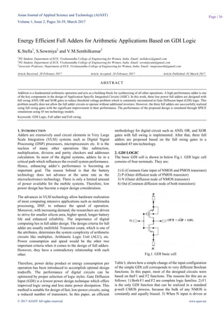
  • 1. Asian Journal of Applied Science and Technology (AJAST) Volume 1, Issue 2, Pages 36-39, March 2017 © 2017 AJAST All rights reserved. www.ajast.net Page | 36 Energy Efficient Full Adders for Arithmetic Applications Based on GDI Logic K.Stella1 , S.Sowmiya2 and V.M.Senthilkumar3 1 PG Student, Department of ECE, Vivekanandha College of Engineering for Women, India. Email: stellakcss@gmail.com 2 PG Student, Department of ECE, Vivekanandha College of Engineering for Women, India. Email: sowmijeyam@gmail.com 3 Associate Professor, Department of ECE, Vivekanandha College of Engineering for Women, India. Email: vmspraneeth@gmail.com Article Received: 20 February 2017 Article Accepted: 28 February 2017 Article Published: 02 March 2017 1. INTRODUCTION Adders are extensively used circuit elements in Very Large Scale Integration (VLSI) systems such as Digital Signal Processing (DSP) processors, microprocessors etc. It is the nucleus of many other operations like subtraction, multiplication, division and parity checkers and addresses calculation. In most of the digital systems, adders lie in a critical path which influences the overall system performance. Hence, enhancing adder‟s performance is becoming an important goal. The reason behind is that the battery technology does not advance at the same rate as the microelectronics technology. There is only a limited amount of power available for the mobile systems. Therefore, low power design has become a major design consideration. The advances in VLSI technology allow hardware realization of most computing intensive applications such as multimedia processing, DSP, to enhance the speed of operation. Moreover, with increasing demand, the researchers are driven to strive for smaller silicon area, higher speed, longer battery life and enhanced reliability. The importance of digital computing lies in full adder design. The design criteria for full adder are usually multifold. Transistor count, which is one of the attributes, determines the system complexity of arithmetic circuits like multiplier, Arithmetic Logic Unit (ALU), etc. Power consumption and speed would be the other two important criteria when it comes to the design of full adders. However, they have a contradictory relationship with each other. Therefore, power delay product or energy consumption per operation has been introduced to accomplish optimal design tradeoffs. The performance of digital circuits can be optimized by proper selection of logic styles. Gate Diffusion Input (GDI) is a lowest power design technique which offers improved logic swing and less static power dissipation. This method is suitable for design of fast, low-power circuits, using a reduced number of transistors. In this paper, an efficient methodology for digital circuit such as AND, OR, and XOR gates with full swing is implemented. After that, three full adders are proposed based on the full swing gates in a standard 45 nm technology. 2. GDI LOGIC The basic GDI cell is shown in below Fig.1. GDI logic cell consists of four terminals. They are: 1) G (Common Gate input of NMOS and PMOS transistor) 2) P (Outer diffusion node of PMOS transistor) 3) N (Outer diffusion node of NMOS transistor) 4) Out (Common diffusion node of both transistors) Fig.1. GDI basic cell Table I, shows how a simple change of the input configuration of the simple GDI cell corresponds to very different Boolean functions. In this paper, most of the designed circuits were based on theF1 and F2 functions. The reasons for this are as follows: 1) Both F1 and F2 are complete logic families. 2) F1 is the only GDI function that can be realized in a standard p-well CMOS process, because the bulk of any NMOS is constantly and equally biased. 3) When N input is driven at ABSTRACT Addition is a fundamental arithmetic operation and acts as a building block for synthesizing of all other operations. A high-performance adder is one of the key components in the design of Application Specific Integrated Circuits (ASIC). In this work, three low power full adders are designed with full swing AND, OR and XOR gates to reduce threshold voltage problem which is commonly encountered in Gate Diffusion Input (GDI) logic. This problem usually does not allow the full adder circuits to operate without additional inverters. However, the three full adders are successfully realized using full swing gates with the significant improvement in their performance. The performance of the proposed design is simulated through SPICE simulations using 45 nm technology models. Keywords: GDI Logic, Full adder and Full swing.
  • 2. Asian Journal of Applied Science and Technology (AJAST) Volume 1, Issue 2, Pages 36-39, March 2017 © 2017 AJAST All rights reserved. www.ajast.net Page | 37 high logic level and P input is at low logic level, the diodes between NMOS and PMOS bulks to Out are directly polarized and there is a short between N and P, resulting in static power dissipation. Table I. Various logic functions of GDI cell for different input configurations 3. PROPOSED FULL ADDERS IN GDI In this section, three proposed full adder designs featuring GDI with full swing logic are discussed with the goal to minimize the circuit complexity and to achieve speed at cascaded operation. The strategy is to avoid threshold voltage losses with the help of full swing gates. 3.1. Basic gates for full adder design The logic function of full adder can be represented as, Sum= A XOR B XOR Cin (1) Cout= A AND B + B AND Cin+ A AND Cin (2) From Eqs. (1) and (2) three basic gates are needed for implementing the function. Fig.2. Full swing gates based on F1 and F2 (a) AND (b) OR and (c) XOR 3.2. Full swing AND, OR and XOR gates using F1 and F2 functions Conventionally universal gates, namely NAND and NOR can be used to realize any logical expression. Similarly, in GDI, two functions are available, namely, F1 (AB) and F2 (A + B) to realize logical expression. These two functions are also suffering from a threshold voltage drop. Swing restoration transistor provided at the output to take care of threshold voltage loss and the schematic of AND, OR and XOR gates using F1 and F2 functions are shown in Fig 2. It increases the transistor count from 2 to 3 for the design of AND and OR yet the full swing operation can be achieved. The choice of F1 and F2 for AND and OR gates will be good since a less number of transistors also provides full swing like CMOS. However, F1 and F2 based XOR gate implementation lacks CMOS based design. The reason might be one of the following: (i) XOR gate based on F1 and F2 needs a total of 9 transistors, which is twice that of the transistors required for GDI logic. Therefore, it cuts off the goal of GDI logic, i.e. function realization using minimal transistor. (ii) Due to increased transistor count, the overall input gate capacitance (Cg) of the XOR function increased since Cg is a direct function of the number of transistor seen by the inputs. (iii) The intermediate nodes can be increased slightly; this might lead to a number of glitches which are the sources of power consumption. The realization of AND and OR gates with full swing can be possible using F1 and F2 functions, respectively, and operate relatively better than conventional design though not suitable for XOR realization. But XOR-XNOR circuits are basic building blocks in various arithmetic circuits such as adders, multipliers, compressors, comparators, etc. They provide an intermediate output to generate the final sum and carry the full adder. Also the importance of XOR-XNOR functions, implementations like an adder and multiplier. Therefore, full swing XOR is necessary to drive successive stages reliably. 3.3. Proposed full swing XOR gate This subsection details about the proposed XOR gate to achieve full swing operation. It acts as one of the basic modules for the realization of three full adder designs and the performance of the designed adders are investigated under full swing XOR gate as one of the modules. The proposed XOR gate uses 4T to provide full swing in the output. The design of XOR gate using GDI logic without and with full swing is shown in Fig 3. The goal is to reduce the circuit complexity and to achieve faster cascaded operation. The techniques presented in the literature directly use supply rail VDD for strong „1‟ and VSS for strong „0‟. But the proposed design does not use supply rails either GND or VDD for obtaining the perfect output. It uses input, but only with proper biasing of a necessary transistor, which may be either PMOS or NMOS. N P G Out Function 0 B A A‟B F1 B 1 A A‟+B F2 1 B A A+B OR B 0 A AB AND C B A A‟B+AC MUX 0 1 A A‟ NOT
  • 3. Asian Journal of Applied Science and Technology (AJAST) Volume 1, Issue 2, Pages 36-39, March 2017 © 2017 AJAST All rights reserved. www.ajast.net Page | 38 Fig.3. XOR gate (a) using GDI logic and (b) proposed design For AB = 00, transistor P1 (PMOS), P3 (NMOS) and P4 (PMOS) conduct. The P3 transistor is responsible for delivering strong „0‟.Likewise, another case when AB = 10, transistor P2 (NMOS), P3(NMOS) and P4 (PMOS) work for the given input, in which P4 passes strong „1‟ to the output. Whereas in other cases, namely AB = 01 and 11, the transistors P3 and P4 do not change the output potential. Hence, the correct output for XOR gate is attained with the proposed design. 4. THREE FULL ADDER DESIGNS The design of GDI full adder with full swing can be made possible with the help of full swing gates such as AND, OR and XOR discussed in the previous section. This design completely eliminates the swing restoration buffers that results in improvement in the performance. Three possible full swing GDI full adders are designed by rewriting the full adder design expression Eqs. (1) and (2). The full adder‟s Sum and Cout expressions are given in Eqs. (3) and (4), respectively. Sum= Cin (A XOR B) +Cin (A XNOR B) (3) Cout= (A XOR B)Cin+ (A XOR B)A (4) Fig.4. Design 1 Full adder Design 1 uses XOR output as an intermediate result. Sum output can be attained by multiplexing the XOR and its inverted version XNOR through Cin input. Cout is obtained by multiplexing the inputs A and Cin whose output is controlled by the selection input. The presence of inverter on the critical path increases the delay of the whole circuit. This design is simple and requires a total of 18 transistors for realizing the full adder function. Design 2 The Sum and Cout expressions are represented in Eqs. 5 and 6, respectively. Sum= A XOR B XOR Cin (5) Cout= Cin (A AND B) + Cin (A OR B) (6) Fig.5. Design 2 Full adder Cout function can be realized with the help of AND and OR gates. AND and OR gates are designed based on F1 and F2, respectively. Multiplexing the AND and OR operation through Carry input Cin helps in Cout realization. The XOR operation on the inputs A, B and Cin achieves Sum function. It requires total 22 transistors. Fig.6. Design 3 Full adder Design 3 It is designed by considering the XOR, AND and OR gates and the Sum and Cout design expressions are given in Eqs. (7) and (8). Sum= A XOR B XOR Cin (7) Cout= A AND B + (A XOR B) Cin (8)
  • 4. Asian Journal of Applied Science and Technology (AJAST) Volume 1, Issue 2, Pages 36-39, March 2017 © 2017 AJAST All rights reserved. www.ajast.net Page | 39 Sum output can be achieved by XORing the inputs A, Band Cin. The output Cout is obtained with the help of AND and OR followed by XOR gate. The realization of AND and OR gate can be done with the help of full swing F1 and F2 gates. The GDI based F1 and F2 enables the implementation of AND and OR with only 3 transistors whereas CMOS needs 6 transistors for achieving the same. The intermediate XOR gate output is used for computing Cout output. So totally, 23 transistors are needed for designing a full adder. The proposed full adder based on Design 1, Design 2 and Design 3 are shown in the above Fig 4, 5, 6. 5. RESULT ANALYSIS Table II. Comparison of Full adders (a) Design 1 is a best possible candidate for the applications in which minimum transistor count and low power is a design requirement. (b) The Design 2 offers minimum delay, so it can be suitable for battery operated and real-time applications. It has slightly increased in transistor count compared with Design 1. (c) Design 3 lies midway between Design 1 and Design 2, and offers lower delay than Design 1. From the obtained results, it can be concluded that all three designs operate with less energy consumption than existing adders taken for comparison. Hence, these designs can be suitable for realizing energy efficient arithmetic applications. 6. CONCLUSION In this work, three full adder designs that use as few as twenty transistors per bit are proposed. The design adopts full swing XOR, AND and OR gates to alleviate the threshold voltage problem and to enhance the driving capability for cascaded operation. The enhanced driving capability also facilitates lower voltage and faster operation which leads to power consumption. The proposed designs are simulated using the SPICE simulation tool at 45 nm technology. The comparison is done in terms of power consumption, propagation delay, and transistor count. REFERENCES [1] A.M. Shams, A.K Darwish and M.A. Bayoumi, “Performance analysis of low power 1-bit CMOS full adder cells”, IEEE Trans. VLSI Syst., Vol.10, No.1, pp. 20–29, 2002. [2] V. Foroutan, M. Taheri , K. Navi and A. Mazreah, “Design of two low power full adder cells using GDI structure and hybrid CMOS logic style”, Integration (Amst), Vol.47, No.1, pp.48–61,2014. [3] A. Morgenshtein, A. Fish And I.A. Wagner, “Gate Diffusion Input (GDI)-A power efficient method for digital combinatorial circuits”, IEEE Trans. VLSI Syst., Vol.10, No.5, pp.566–581, 2002. [4] R. Uma and P. Dhavachelvan, “Modified gate diffusion input technique: a new technique for enhancing performance in full adder circuits”, Proc. ICCCS, pp.74–81, 2012. [5] A. Morgenshtein , I. Shwartz and A. Fish, “Full swing Gate Diffusion Input (GDI) logic case study for low power CLA adder design”, Integration (Amst), Vol.47, No.1, pp.62-70, 2014. [6] M. Aguirre-Hernandez and M. Linares-Aranda, “CMOS full adders for energy efficient arithmetic applications”, IEEE Trans. VLSI Syst., Vol.19, No.4, pp. 718–72, 2011. [7] I. Hassoune, D. Flandre, I. O‟Connor and J. Legat, “ULPFA: a new efficient design of a power-aware full adder”, IEEE Trans. Circuits Syst., Vol.57, No.8, pp.2066–2074, 2010. [8] P. M. Lee, C. H Hsu., Y. H. Hung, “Novel 10-T full adders realized by GDI structure”, Proc. IEEE Int. Symp. Integr. Circuits, pp.115–118, 2007. [9] M. Maeen, V. Foroutan and K. Navi, “On the design of low power 1 –bit full adder cell”, IEICE Electron. Expert. Vol.6, No.16, pp.1148–1154, 2009. [10] R. Patel H. Parasar and M. Wajid, “Faster arithmetic and logical unit CMOS design with reduced number of transistors”, Proc. of Intl. Conf. on Advances in Communication, Network and Computing, Vol.142, pp.519–522, 2011. [11] S. Purohit and M. Margala, “Investigating the impact of logic and implementation for full adder performance”, IEEE Trans. VLSI Syst., Vol.20, No.7, pp.1327–1331, 2012. [12] G. Ramana Murthy, C. Senthil Pari, P. Velraj Kumar and T.S. Lim, “A new 6-T multiplexer based full adder for low power and leakage current optimization”, IEICE Electronics Express, Vol.9, No.17, pp.1434–1441, 2012. [13] R. Singh and S. Akashe, “Modeling and analysis of low power 10T full adder with reduced ground noise”, J. Circuits Syst. Comput., Vol.23, No.14, pp.1–14, 2014.