
Recommended
Recommended
More Related Content
What's hot
What's hot (20)
Similar to Performance evaluation of full adder
Similar to Performance evaluation of full adder (20)
More from IOSRJECE
More from IOSRJECE (20)
Recently uploaded
Recently uploaded (20)
Performance evaluation of full adder
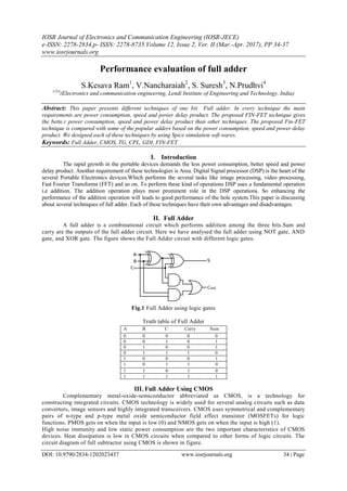
- 1. IOSR Journal of Electronics and Communication Engineering (IOSR-JECE) e-ISSN: 2278-2834,p- ISSN: 2278-8735.Volume 12, Issue 2, Ver. II (Mar.-Apr. 2017), PP 34-37 www.iosrjournals.org DOI: 10.9790/2834-1202023437 www.iosrjournals.org 34 | Page Performance evaluation of full adder S.Kesava Ram1 , V.Nancharaiah2 , S. Suresh3 , N.Prudhvi4 1234 (Electronics and communication engineering, Lendi Institute of Engineering and Technology, India) Abstract: This paper presents different techniques of one bit Full adder. In every technique the main requirements are power consumption, speed and power delay product. The proposed FIN-FET technique gives the bette.r power consumption, speed and power delay product than other techniques. The proposed Fin-FET technique is compared with some of the popular adders based on the power consumption, speed and power delay product. We designed each of these techniques by using Spice simulation soft wares. Keywords: Full Adder, CMOS, TG, CPL, GDI, FIN-FET. I. Introduction The rapid growth in the portable devices demands the less power consumption, better speed and power delay product. Another requirement of these technologies is Area. Digital Signal processor (DSP) is the heart of the several Portable Electronics devices.Which performs the several tasks like image processing, video processing, Fast Fourier Transforms (FFT) and so on. To perform these kind of operations DSP uses a fundamental operation i.e addition. The addition operation plays most prominent role in the DSP operations. So enhancing the performance of the addition operation will leads to good performance of the hole system.This paper is discussing about several techniques of full adder. Each of these techniques have their own advantages and disadvantages. II. Full Adder A full adder is a combinational circuit which performs addition among the three bits.Sum and carry are the outputs of the full adder circuit. Here we have analysed the full adder using NOT gate, AND gate, and XOR gate. The figure shows the Full Adder circuit with different logic gates. Fig.1 Full Adder using logic gates Truth table of Full Adder III. Full Adder Using CMOS Complementary metal-oxide-semiconductor abbreviated as CMOS, is a technology for constructing integrated circuits. CMOS technology is widely used for several analog circuits such as data convertors, image sensors and highly integrated transceivers. CMOS uses symmetrical and complementary pairs of n-type and p-type metal oxide semiconductor field effect transistor (MOSFETs) for logic functions. PMOS gets on when the input is low (0) and NMOS gets on when the input is high (1). High noise immunity and low static power consumption are the two important characteristics of CMOS devices. Heat dissipation is low in CMOS circuits when compared to other forms of logic circuits. The circuit diagram of full subtractor using CMOS is shown in figure. A B C Carry Sum 0 0 0 0 0 0 0 1 0 1 0 1 0 0 1 0 1 1 1 0 1 0 0 0 1 1 0 1 1 0 1 1 0 1 0 1 1 1 1 1
- 2. Performance evaluation of full adder DOI: 10.9790/2834-1202023437 www.iosrjournals.org 35 | Page Fig. Schematic Diagram of Full adder(CMOS) Fig . Out put Wave forms IV. Full Adder Using CPL The complex logics can be alternatively implemented using CPL(complementary pass transistor logic). CPL is extremely fast and efficient. Some of the examples of CPL circuits are shown in figure 5. Fig. Realization of Logic Gates using CPL method By eliminating the redundant transistors, it reduces the count of transistors used to make different logic gates. In order to pass logic levels between nodes of a circuit the transistors are used as switches. The main principle involved in CPL is the use of NMOS pass transistor for logic organisation and elimination of the PMOS latch. The circuit diagram of full adder using CPL is shown in figure. Fig. Schematic Diagram of Full adder (CPL) Fig. Output Wave forms of CPL method
- 3. Performance evaluation of full adder DOI: 10.9790/2834-1202023437 www.iosrjournals.org 36 | Page V. Full Adder Using GDI GDI(gate diffusion input) is a technique of low power digital circuit design which reduces power consumption, delay and area. It is based on the use of a simple cell as shown in figure. It is similar to that of CMOS invertor but there are some differences:GDI cell contains three inputs. They are G(common gate input of NMOS and PMOS), P(input to the source/drain of PMOS) and N(input to the source/drain of NMOS). Fig.GDI cell GDI technique allows implementation of a wide range of complex logic functions using only two transistors. This method produces designs which are fast with low power dissipation by using less number of transistors. The circuit diagram of full subtractor using GDI technique is shown in figure 8. Fig. Schematic Diagram of Full Adder (GDI) Fig. Output Wave forms of the GDI Technique VI. Full Adder Using Finfet Conventional MOSFETs have inherent problems of large leakage currents from gate to channel and increasingly unreliable transistor characteristics. To cater these problems, FinFET transistor technology has been developed which has cast a profound impact on the semiconductor industry. It provides a new pathway for Moore's Law beyond 20nm as they have much better performance and reduced power consumption compared to planar transistors. The next few years should be very interesting as the benefits of this technology are seen in products from smart phones to servers. The below figures shows the FinFET layout diagrams. Fig: FinFET Layout Fig: Schematic view of Full adder using FinFET The Full adder using the FinFET is shown above and it shown the lower power consumption when compared to the CMOS logic.
- 4. Performance evaluation of full adder DOI: 10.9790/2834-1202023437 www.iosrjournals.org 37 | Page VII. Comparison Of Different Full Adder Techniques We have designed full adder in different techniques. Each technique has its own advantages and disadvantages. Below table shows the comparison of all these techniques. Table. Power consumed by each Technique Technique Power consumption(W) CMOS 6.474195e-003 GDI 4.242147e-004 CPL 1.900524e-003 FinFET 190.9uw VIII. Conclusion From the table which is show above gives the complete Performance Evolution of the Full adder. Finally we can conclude that FinFET technique is best technique in terms of the power consumption. It consumes and dissipates less power. Acknowledgment I would like to express my gratitude towards my guide (V. Nancharaiah sir) for their kind cooperation and encouragement which help me in completion of this project. My thanks and appreciations also go to my team meats in developing the project and people who have willingly helped me out with their abilities. References Journal Papers: [1]. Low voltage high performance hybrid full adder Pankaj Kumar *, Rajender Kumar Sharma National Institute of Technology, Kurukshetra, India [2]. High performance full subtractor using floating-gate MOSFET Roshani Gupta, Rockey Gupta, Susheel Sharma [3]. Combinational Circuits Using Transmission Gate Logic For Power Optimization G.Naveen Balaji1 V.Aathira2 K. Ambhikavathi3 S. Geethiga4 R. Havin5 1Assistant Professor, Department of ECE, SNS College of Technology, Coimbatore, India [4]. Gate-diffusion input (gdi) - a technique for low power design of digital circuits: analysis and characterization Arkadiy Morgenshtein’, Alexander Fish2 and Israel A. Wagner’ [5]. High performance full subtractor using floating-gate MOSFET Roshani Gupta, Rockey Gupta, Susheel Sharma [6]. Finfet- Benefits, Drawbacks and Challenges Mayur Bhole*1, Aditya Kurude2, Sagar Pawar3 *1, 2, 3BE (E&TC), PVG’s COET, Pune, India [7]. S. Goel, A. Kumar, M.A. Bayoumi, Design of robust, energy-efficient full adders For deep-submicrometer design using hybrid- CMOS logic style, IEEE Trans. Very Large Scale Integr. (VLSI) Syst. 14 (12) (2006) 1309–1321. [8]. P. Bhattacharyya, B. Kundu, S. Ghosh, V. Kumar, A. Dandapat, Performance Analysis of a low-power high-speed hybrid 1-bit full adder circuit, 2014. [9]. Z. Abid, H. El-Razouk, D. El-Dib, Low power multipliers based on new hybrid Full adders, Microelectr. J. 39 (12) (2008) 1509– 1515. [10]. S. Goel, M. Elgamel, M. Bayoumi, Y. Hanafy, Design methodologies for high performance Noise-tolerant XOR-XNOR circuits, IEEE Trans. Circ. Syst. I Reg. Papers 53 (4) (2006) 867–878. [11]. K. Navi, M. Maeen, V. Foroutan, S. Timarchi, O. Kavehei, A novel low-power Full-adder cell for low voltage, Integration 42 (4) (2009) 457–467. [12]. K. Navi, V. Foroutan, M. Rahimi Azghadi, M. Maeen, M. Ebrahimpour, M. Kaveh, Et al., A novel low-power full-adder cell with new technique in designing logical Gates based on static CMOS inverter, Microelectr. J. 40 (10) (2009) 1441–1448.