Graduate Outcomes Presentation Slides - English (v3).pptx
Bustran
1. Bus Cycles (Chap. 7)
• Data Transfer from x86 to/from Memory or I/O Device
• Occurs Via System (PC) Bus
– 4 System Bus Clock Periods for 8086/8088/80286
(T1, T2, T3, T4)
– 2 System Bus Clock Periods for 386+
(T1, T2)
• Pins on x86 Package Connected to Memory or I/O Interface
• Synchronous Bus
– “Clocked” Bus
– Less Than CPU Clock Speed for Pentium+
(except for 60, 66 and 75 MHz Pentiums)
• 75 MHz Pentium Not Too Popular Since 50 MHz Bus
and 1.5x Multiplier
– Better Performance from 60, 66 MHz Pentiums!
• Motherboard Circuit Generates Bus Clock Signal
– CPU Contains a Clock Multiplier Circuit Internally
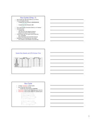
System Bus Speeds and CPU Access Time
System Clock CPU Access Time
Processor
Frequency (MHz) Period (ns) T States Time (ns)
8088 4.77 209 2.3 480
8086 10 100 2.3 230
80286 12.5 80 2.3 184
80386 33 33 1.5 49.5
80486 50 20 1.5 30
Pentium 66 15 1.5 22.5
Pentium Pro 66 15 1.5 22.5
Pentium MMX* 66 15 1.5 22.5
Pentium II* 100 10 1.5 20
Pentium III* 133 7.5 1.5 15
*CPU Core Clock is Generated by Internal Multiplier Circuit
Bus Cycle
• A Single “Transaction” or Data Transfer
• One or More Bus Clock Periods
– 4 System Bus Clock Periods for 8086/8088
• “Read Cycle” is Data Transfer FROM Memory(I/O) TO CPU
• “Write Cycle” is Data Transfer FROM CPU TO Memory(I/O)
1
2. T States
(8088/8086/80286)
T1 STATE (Address Out State)
• CPU Drives Valid Address on Address Bus
T2 STATE (Transaction Type)
• READ:
– IOR or MEMR go Active
• WRITE:
– IOW or MEMW and Data Bus go Active
T3 STATE (Memory or I/O Respond)
• READ:
– CPU “waits” for Memory (or I/O) to Drive Data Bus
• WRITE:
– CPU Continues to Drive Data Bus
T4 STATE (Data Latch State)
• READ:
– CPU Latches Data Bus Signals into Register
• WRITE:
– CPU Drives Data Until End of T4 Allowing Memory (or I/O) to Latch Data Bus Signals in*
*Memory (or I/O device) Typically Uses the Rising Edge of MEMW (or IOW) as a Latch Signal
Access Time
MEMORY ACCESS TIME tAccess Memory
• Time that Elapses from Receipt of Valid Address Until Valid Data is
Present on the Data Bus
• This is a READ Access Time
CPU ACCESS TIME tAccess Processor
• Time from Driving Valid Address Out until T4 When Data Bus Signals Latched
• This is Specified by CPU Manufacturer
• Intel Specified This as 2.3 T States for 8088/8086/80186/80286
• Intel Specified This as 1.5 T States for 386+
tAccess Processor > tAccess Memory
EXAMPLE: IBM XT Using 8088 with 4.77 MHz Clock
• tAccess Processor = 2.3T = (2.3)(1/4,770,000) = 481ns
• State of the Art Memory Access Times were in the 200-300 ns Range
Slow Memory
• “Slow Memory” is Memory with Access Time Close to that of Processor
• Memory can’t Supply Data Fast Enough to Meet the 2.3T (or 1.5T) Specification
• 3 Courses of Action in this Case:
1) Decrease System Clock Frequency
– “Turbo” Switch
– Not Popular Since Everyone Wants “Turbo” On Always
2) Buy Faster Memory
– May Not Yet Exist
– May be Too Expensive (Priced a 128MB PC133 DIMM Lately???)
3) Memory Outputs a “Wait” Signal
– x86 has a READY Input Line on Control Bus
– READY Input “Checked” During T3
– If READY is Inactive (LOW), Additional T3 States are Added
– These Additional T3 States are Called “Wait States”
2
3. 8086/8088 Read Cycle with 1 Wait State
T1 T2 T3 Tw T4
Address Bus
MEMR or IOR
READY
Data Bus
• n Wait States Adds n Clock Cycles of Delay to tAccess Processor
386+ Bus Cycles
• New CPU Output W/R Replaces MEMR, IOR, MEMW, IOW
• New CPU Input READY Replaces READY
• 2 State Bus Cycle T1 and T2 Only
• W/R Asserted in T1
– (as compared to MEMR, MEMW, IOR, IOW in T2)
• Data Latched in T2 if READY is Low
• Wait State Occurs if READY is High in T2
• CPU Specified as 1.5 T
486+ Bus Cycle
3
4. System Bus Speeds and CPU Access Time
System Clock CPU Access Time
Processor
Frequency (MHz) Period (ns) T States Time (ns)
8088 4.77 209 2.3 480
8086 10 100 2.3 230
80286 12.5 80 2.3 184
80386 33 33 1.5 49.5
80486 50 20 1.5 30
Pentium 66 15 1.5 22.5
Pentium Pro 66 15 1.5 22.5
Pentium MMX* 66 15 1.5 22.5
Pentium II* 100 10 1.5 20
Pentium III* 133 7.5 1.5 15
*CPU Core Clock is Generated by Internal Multiplier Circuit
Need for SRAM Cache
• Table Indicates CPU Access Time as Bus Clock Increases
• In 386+ the CPU Access Times are Less Than 50 ns
• Modern DRAM Access Times are 60-80ns
• To Avoid “Wait” States in Every Bus Cycle use SRAM Cache
– 6-15ns Access Time
– Can Achieve 95% Hit Rates (after cold start)
Burst Cycles – 486+
• 2T Cycles Read/Write 1 Quantity Data
– (Byte, Word, DoubleWord, QuadWord)
– (16-86/88/186/286, 32-386/486 and 64-Pentium+ bit Data Buses)
• To Allow Fast Cache Fills, Added “Burst Mode”
• Cache Line is Several QuadWords
• “Burst Cycle”
– 2T for First Quantity
– 1T for Subsequent Quantities
4
5. 486 Burst Cycles Characteristics
• No Write Bursts Supported
• Maximum Read Burst is 16 Bytes (1 Cache Line)
• “Aligned” Data Only
– (begin at address xxxx002 end at address xxxx112)
• Possible Sequences:
xxxx0h, xxxx1h, xxxx2h, xxxx3h T1, T2
xxxx4h, xxxx5h, xxxx6h, xxxx7h TB1
xxxx8h, xxxx9h, xxxxah, xxxxbh TB2
xxxxch, xxxxdh, xxxxeh, xxxxfh TB3
• Requires 5T to Read 16 Bytes (Instead of 8!)
• Uses BRDY# and BLAST# - New Control Bus Signals
• Four Aligned Access Possibilities
0-4-8-C 4-8-C-0 8-C-0-4 C-0-4-8
Pentium Burst Cycles Characteristics
• Supports Read and Write Bursts
• 32 Byte Maximum Burst (1 Cache Line=32 Bytes)
• “Aligned” Data Only
– (begin at address xxxx0002 end at address xxxx1112)
• Four Aligned Access Possibilities
0-8-10-18 8-10-18-0 10-18-0-8 18-0-8-10
Subsequent Burst Cycles
• Previously We Saw 2T+T+T+T (=T1+T2+TB1+TB2+TB3)
Required For 16 Byte Transfer (in 486)
• This is a 2-1-1-1 Burst
• Subsequent Bursts
2-1-1-1; 2-1-1-1; 2-1-1-1; …;2-1-1-1
5
6. Pipelined Burst Cycles
• Pentium Allows Next “Burst Address” to be Asserted
in Last Burst Cycle
• Subsequent Bursts
2-1-1-1*; 1**-1-1-1*; 1**-1-1-1*; …;1**-1-1-1
*Address for Next Asserted Here Instead of Next T1
**Can Think of This as a T2 with the T1 Skipped
Memory Access Width
• May Not Need “Full Data Bus Width” in an Access
e.g. mov al, [0000]
• Data Bus Widths Vary
8088-8bits; 8086/186/286-16bits; 80386/486-32bits; Pentium+-64bits
• Solution is to Use “Byte Enable” Signals
• Output Signals (in Control Bus) of x86
8088/86/186/286 Uses BHE and A0
80386/486 Uses BE3-BE0
Pentium+ Uses BE7-BE0
Byte Enable Examples
6
7. Alignment
• IF Requested Bytes Within 1 Doubleword (386,486) or
1 Quadword (Pentium+) THEN
Access is ALIGNED and Requires 1 Bus Cycle
• IF Requested Bytes Cross Address Boundary THEN
Access is MISALIGNED and Requires 2 Bus Cycles
Byte Selection Example
Data Transfer Rate-CPU Bandwidth
# Bytes _ Per _ Bus _ Cycle
BWCPU =
Time _ Per _ Bus _ Cycle
• Units are Bytes/Sec
(Loosely See This Specification Referred to in Hz)
• 1 Bus Cycle: n
n × Tclock =
f
n ≡ Number _ of _ T _ States
# Bytes _ Per _ Cycle × f
BWCPU =
n
7
8. Bandwidth Example
8088 System @ 4.77 MHz External Clock
Data Bus = 1 Byte 4T Transfer
BW=[(1 byte)(4.77 MHz)]/(4)=1.19 MB/s
Pentium II @ 100 MHz External Clock
Data Bus = 8 Bytes 2T Transfer
BW=[(8 bytes)(100 MHz)]/(2)=400.0 MB/s
Increase in BW is 33,513% !!!!!!!!!!
8