SlideShare a Scribd company logo
1 of 23
Sequential circuits
The combinational circuit does not use any
memory. Hence the previous state of input does not
have any effect on the present state of the circuit. But
sequential circuit has memory so output can vary
based on input. This type of circuits uses previous
input, output, clock and a memory element.
Block Diagram
• Flip Flop
• Flip flop is a sequential circuit which generally
samples its inputs and changes its outputs
only at particular instants of time and not
continuously. Flip flop is said to be edge
sensitive or edge triggered rather than being
level triggered like latches.
The NAND Gate SR Flip-Flop
• The simplest way to make any basic single bit set-
reset SR flip-flop is to connect together a pair of
cross-coupled 2-input NAND gates as shown
• To form a Set-Reset Bistable also known as an
active LOW SR NAND Gate Latch, so that there is
feedback from each output to one of the other
NAND gate inputs.
• This device consists of two inputs, one called the
Set, S and the other called the Reset, R with two
corresponding outputs Q and its inverse or
complement Q (not-Q) as shown below.
• Truth Table for this Set-Reset Function
• State S R Q Q’ Description
• Set 1 0 0 1 set Q’ » 1
1 1 0 1 no change
• Reset 0 1 1 0 reset Q’ » 0
1 1 1 0 no change
• Invalid 0 0 1 1 Invalid Condition
• Clocked or Enabled S-R Flip Flop
• It is basically S-R latch using NAND gates with
an additional enable input.
• It is also called as level triggered SR-FF. For
this, circuit in output will take place if and only
if the enable input (E) is made active.
• In short this circuit will operate as an S-R latch
if E = 1 but there is no change in the output if
E = 0.
Block Diagram
Circuit diagram
• Truth Table
Operation
• Condition Operation S = R = 0 : No change If S = R = 0
then output of NAND gates 3 and 4 are forced to
become 1.
• Hence R' and S' both will be equal to 1. Since S' and R'
are the input of the basic S-R latch using NAND gates,
there will be no change in the state of outputs.
• S = 0, R = 1, E = 1 Since S = 0, output of NAND-3 i.e. R'
= 1 and E = 1 the output of NAND-4 i.e. S' = 0.
• Hence Qn+1 = 0 and Qn+1 bar = 1. This is reset
condition.
• S = 1, R = 0, E = 1 Output of NAND-3 i.e. R' = 0
and output of NAND-4 i.e. S' = 1.
• Hence output of S-R NAND latch is Qn+1 = 1
and Qn+1 bar = 0. This is the reset condition.
• S = 1, R = 1, E = 1 As S = 1, R = 1 and E = 1, the
output of NAND gates 3 and 4 both are 0 i.e. S'
= R' = 0.
• Hence the Race condition will occur in the
basic NAND latch.
JK Flip flop
A JK flip-flop has two inputs similar to that of
RS flip-flop. We can say JK flip-flop is a refinement
of RS flip-flop. JK means Jack Kilby, a Texas
instrument engineer who invented IC. The two
inputs of JK Flip-flop is J (set) and K (reset). A JK
flip-flop is nothing but a RS flip-flop along with
two AND gates which are augmented to it.
• The flip-flop is constructed in such a way that
the output Q is ANDed with K and CP.
• This arrangement is made so that the flip-flop
is cleared during a clock pulse only if Q was
previously 1.
• Similarly Q’ is ANDed with J and CP, so that the
flip-flop is cleared during a clock pulse only if
Q’ was previously 1.
Master Slave JK Flip Flop
• Master slave JK FF is a cascade of two S-R FF
with feedback from the output of second to
input of first.
• Master is a positive level triggered. But due to
the presence of the inverter in the clock line,
the slave will respond to the negative level.
• Hence when the clock = 1 (positive level) the
master is active and the slave is inactive.
• Whereas when clock = 0 (low level) the slave
is active and master is inactive.
Circuit Diagram & Truthtable
Operation
• J = K = 0 (No change) When clock = 0, the slave becomes active and master is
inactive. But since the S and R inputs have not changed, the slave outputs will also
remain unchanged. Therefore outputs will not change if J = K =0.
• J = 0 and K = 1 (Reset) Clock = 1 − Master active, slave inactive. Therefore outputs
of the master become Q1 = 0 and Q1 bar = 1. That means S = 0 and R =1.
• Clock = 0 − Slave active, master inactive. Therefore outputs of the slave become Q
= 0 and Q bar = 1.
• Again clock = 1 − Master active, slave inactive. Therefore even with the changed
outputs Q = 0 and Q bar = 1 fed back to master, its output will be Q1 = 0 and Q1
bar = 1. That means S = 0 and R = 1.
• Hence with clock = 0 and slave becoming active the outputs of slave will remain Q
= 0 and Q bar = 1. Thus we get a stable output from the Master slave.
• J = 1 and K = 0 (Set) Clock = 1 − Master active, slave inactive. Therefore outputs of
the master become Q1 = 1 and Q1 bar = 0. That means S = 1 and R =0.
• Clock = 0 − Slave active, master inactive. Therefore outputs of the slave become Q
= 1 and Q bar = 0.
• Again clock = 1 − then it can be shown that the outputs of the slave are stabilized
to Q = 1 and Q bar = 0.
• J = K = 1 (Toggle) Clock = 1 − Master active, slave inactive. Outputs of master will
toggle. So S and R also will be inverted.
• Clock = 0 − Slave active, master inactive. Outputs of slave will toggle.
• These changed output are returned back to the master inputs. But since clock = 0,
the master is still inactive. So it does not respond to these changed outputs. This
avoids the multiple toggling which leads to the race around condition. The master
slave flip flop will avoid the race around condition.
Delay Flip Flop / D Flip Flop
• Delay Flip Flop or D Flip Flop is the simple gated S-R latch
with a NAND inverter connected between S and R inputs.
• It has only one input. The input data is appearing at the
output after some time. Due to this data delay between
i/p and o/p, it is called delay flip flop.
• S and R will be the complements of each other due to
NAND inverter. Hence S = R = 0 or S = R = 1, these input
condition will never appear.
• This problem is avoid by SR = 00 and SR = 1 conditions.
Block Diagram
Circuit Diagram
Truth table
Operation
• 1 E = 0 Latch is disabled. Hence no change in output.
• 2 E = 1 and D = 0 If E = 1 and D = 0 then S = 0 and R = 1. Hence
irrespective of the present state, the next state is Qn+1 = 0 and
Qn+1 bar = 1. This is the reset condition.
• 3 E = 1 and D = 1 If E = 1 and D = 1, then S = 1 and R = 0. This
will set the latch and Qn+1 = 1 and Qn+1 bar = 0 irrespective of
the present state.
Toggle Flip Flop / T Flip Flop
• Toggle flip flop is basically a JK flip flop with J
and K terminals permanently connected
together.
• It has only input denoted by T as shown in the
Symbol Diagram. The symbol for positive edge
triggered T flip flop is shown in the Block
Diagram.
Block Diagram
Circuit Diagram
Truth table
• Operation
• T = 0, J = K = 0 The output Q and Q bar won't
change.
• T = 1, J = K = 1 Output will toggle
corresponding to every leading edge of clock
signal.

More Related Content

What's hot

What's hot (19)

SEQUENTIAL LOGIC CIRCUITS (FLIP FLOPS AND LATCHES)
SEQUENTIAL LOGIC CIRCUITS (FLIP FLOPS AND LATCHES)SEQUENTIAL LOGIC CIRCUITS (FLIP FLOPS AND LATCHES)
SEQUENTIAL LOGIC CIRCUITS (FLIP FLOPS AND LATCHES)
 
Synchronous Sequential Logic Unit 4
Synchronous Sequential Logic Unit 4Synchronous Sequential Logic Unit 4
Synchronous Sequential Logic Unit 4
 
FYBSC IT Digital Electronics Unit IV Chapter II Sequential Circuits- Flip-Flops
FYBSC IT Digital Electronics Unit IV Chapter II Sequential Circuits- Flip-FlopsFYBSC IT Digital Electronics Unit IV Chapter II Sequential Circuits- Flip-Flops
FYBSC IT Digital Electronics Unit IV Chapter II Sequential Circuits- Flip-Flops
 
COUNTERS(Synchronous & Asynchronous)
COUNTERS(Synchronous & Asynchronous)COUNTERS(Synchronous & Asynchronous)
COUNTERS(Synchronous & Asynchronous)
 
Counter
CounterCounter
Counter
 
Sequential circuit
Sequential circuitSequential circuit
Sequential circuit
 
Trts d flip flop1
Trts d flip flop1Trts d flip flop1
Trts d flip flop1
 
SEQUENTIAL CIRCUITS [Flip-flops and Latches]
SEQUENTIAL CIRCUITS [Flip-flops and Latches]SEQUENTIAL CIRCUITS [Flip-flops and Latches]
SEQUENTIAL CIRCUITS [Flip-flops and Latches]
 
Digital clock (mod counters)using DSCH (DIGITAL SCHEMATIC) by Gaurav Raikar
Digital clock (mod counters)using DSCH (DIGITAL SCHEMATIC) by Gaurav RaikarDigital clock (mod counters)using DSCH (DIGITAL SCHEMATIC) by Gaurav Raikar
Digital clock (mod counters)using DSCH (DIGITAL SCHEMATIC) by Gaurav Raikar
 
Ripple counter
Ripple counterRipple counter
Ripple counter
 
Counter And Sequencer Design- Student
Counter And Sequencer Design- StudentCounter And Sequencer Design- Student
Counter And Sequencer Design- Student
 
MSI Counters
MSI CountersMSI Counters
MSI Counters
 
Synchronous Counter
Synchronous Counter Synchronous Counter
Synchronous Counter
 
Ece221 Ch7 Part1
Ece221 Ch7 Part1Ece221 Ch7 Part1
Ece221 Ch7 Part1
 
Basics Counters
Basics Counters Basics Counters
Basics Counters
 
Race around and master slave flip flop
Race around and master slave flip flopRace around and master slave flip flop
Race around and master slave flip flop
 
Chapter 5 counter
Chapter 5 counterChapter 5 counter
Chapter 5 counter
 
Counters
CountersCounters
Counters
 
555 timer
555 timer555 timer
555 timer
 

Similar to Flipflop r012

Digital Electronics Unit_3.pptx
Digital Electronics Unit_3.pptxDigital Electronics Unit_3.pptx
Digital Electronics Unit_3.pptxThapar Institute
 
Sequentialcircuits
SequentialcircuitsSequentialcircuits
SequentialcircuitsRaghu Vamsi
 
MASTER SLAVE JK FLIP FLOP & T FLIP FLOP
MASTER SLAVE JK FLIP FLOP & T FLIP FLOPMASTER SLAVE JK FLIP FLOP & T FLIP FLOP
MASTER SLAVE JK FLIP FLOP & T FLIP FLOPSmit Shah
 
Sequential logic circuits flip-flop pt 1
Sequential logic circuits   flip-flop pt 1Sequential logic circuits   flip-flop pt 1
Sequential logic circuits flip-flop pt 1Sarah Sue Calbio
 
SEQUENTIAL CIRCUITS [FLIP FLOPS AND LATCHES]
SEQUENTIAL CIRCUITS [FLIP FLOPS AND LATCHES]SEQUENTIAL CIRCUITS [FLIP FLOPS AND LATCHES]
SEQUENTIAL CIRCUITS [FLIP FLOPS AND LATCHES]SUBHA SHREE
 
Flip flop slide
Flip flop slideFlip flop slide
Flip flop slidejyothir19
 
Digital Electronics R-S, J-K flip flop etc.pptx
Digital Electronics R-S, J-K  flip flop etc.pptxDigital Electronics R-S, J-K  flip flop etc.pptx
Digital Electronics R-S, J-K flip flop etc.pptxProfVilasShamraoPati
 
UNIT - III.pptx
UNIT - III.pptxUNIT - III.pptx
UNIT - III.pptxamudhak10
 
J - K & MASTERSLAVE FLIPFLOPS
J - K & MASTERSLAVE FLIPFLOPSJ - K & MASTERSLAVE FLIPFLOPS
J - K & MASTERSLAVE FLIPFLOPSKrishma Parekh
 
Flip Flop | Counters & Registers | Computer Fundamental and Organization
Flip Flop | Counters & Registers | Computer Fundamental and OrganizationFlip Flop | Counters & Registers | Computer Fundamental and Organization
Flip Flop | Counters & Registers | Computer Fundamental and OrganizationSmit Luvani
 
08 Latches and Flipflops.pdf
08 Latches and Flipflops.pdf08 Latches and Flipflops.pdf
08 Latches and Flipflops.pdfDSOOP
 
Latch Introduction & RS Latch
Latch Introduction &  RS LatchLatch Introduction &  RS Latch
Latch Introduction & RS LatchEasy n Inspire L
 
best slides latches.pdf
best slides latches.pdfbest slides latches.pdf
best slides latches.pdfAreebaShoukat4
 
Flipflops and Excitation tables of flipflops
Flipflops and Excitation tables of flipflopsFlipflops and Excitation tables of flipflops
Flipflops and Excitation tables of flipflopsstudent
 

Similar to Flipflop r012 (20)

Digital Electronics Unit_3.pptx
Digital Electronics Unit_3.pptxDigital Electronics Unit_3.pptx
Digital Electronics Unit_3.pptx
 
Sequential
SequentialSequential
Sequential
 
Sequentialcircuits
SequentialcircuitsSequentialcircuits
Sequentialcircuits
 
MASTER SLAVE JK FLIP FLOP & T FLIP FLOP
MASTER SLAVE JK FLIP FLOP & T FLIP FLOPMASTER SLAVE JK FLIP FLOP & T FLIP FLOP
MASTER SLAVE JK FLIP FLOP & T FLIP FLOP
 
Sequential circuits
Sequential circuitsSequential circuits
Sequential circuits
 
Sequential logic circuits flip-flop pt 1
Sequential logic circuits   flip-flop pt 1Sequential logic circuits   flip-flop pt 1
Sequential logic circuits flip-flop pt 1
 
SEQUENTIAL CIRCUITS [FLIP FLOPS AND LATCHES]
SEQUENTIAL CIRCUITS [FLIP FLOPS AND LATCHES]SEQUENTIAL CIRCUITS [FLIP FLOPS AND LATCHES]
SEQUENTIAL CIRCUITS [FLIP FLOPS AND LATCHES]
 
Flip flop slide
Flip flop slideFlip flop slide
Flip flop slide
 
Digital Electronics R-S, J-K flip flop etc.pptx
Digital Electronics R-S, J-K  flip flop etc.pptxDigital Electronics R-S, J-K  flip flop etc.pptx
Digital Electronics R-S, J-K flip flop etc.pptx
 
Chapter 6: Sequential Logic
Chapter 6: Sequential LogicChapter 6: Sequential Logic
Chapter 6: Sequential Logic
 
UNIT - III.pptx
UNIT - III.pptxUNIT - III.pptx
UNIT - III.pptx
 
J - K & MASTERSLAVE FLIPFLOPS
J - K & MASTERSLAVE FLIPFLOPSJ - K & MASTERSLAVE FLIPFLOPS
J - K & MASTERSLAVE FLIPFLOPS
 
Flip flops
Flip flopsFlip flops
Flip flops
 
Flip Flop | Counters & Registers | Computer Fundamental and Organization
Flip Flop | Counters & Registers | Computer Fundamental and OrganizationFlip Flop | Counters & Registers | Computer Fundamental and Organization
Flip Flop | Counters & Registers | Computer Fundamental and Organization
 
Flipflop
FlipflopFlipflop
Flipflop
 
08 Latches and Flipflops.pdf
08 Latches and Flipflops.pdf08 Latches and Flipflops.pdf
08 Latches and Flipflops.pdf
 
Latch Introduction & RS Latch
Latch Introduction &  RS LatchLatch Introduction &  RS Latch
Latch Introduction & RS Latch
 
best slides latches.pdf
best slides latches.pdfbest slides latches.pdf
best slides latches.pdf
 
Flip flop
Flip flopFlip flop
Flip flop
 
Flipflops and Excitation tables of flipflops
Flipflops and Excitation tables of flipflopsFlipflops and Excitation tables of flipflops
Flipflops and Excitation tables of flipflops
 

More from arunachalamr16

08 logic simplification
08 logic simplification08 logic simplification
08 logic simplificationarunachalamr16
 
Boolean variables r010
Boolean variables   r010Boolean variables   r010
Boolean variables r010arunachalamr16
 
Central processing unit and stack organization r013
Central processing unit and stack organization   r013Central processing unit and stack organization   r013
Central processing unit and stack organization r013arunachalamr16
 
Combinational circuits r011
Combinational circuits   r011Combinational circuits   r011
Combinational circuits r011arunachalamr16
 
Binary coded decimal r004
Binary coded decimal   r004Binary coded decimal   r004
Binary coded decimal r004arunachalamr16
 
Digital fundamendals r001a
Digital fundamendals r001aDigital fundamendals r001a
Digital fundamendals r001aarunachalamr16
 
18 pc09 1.2_ digital logic gates _ boolean algebra_basic theorems
18 pc09 1.2_ digital logic gates _ boolean algebra_basic theorems18 pc09 1.2_ digital logic gates _ boolean algebra_basic theorems
18 pc09 1.2_ digital logic gates _ boolean algebra_basic theoremsarunachalamr16
 
Error detection and correction codes r006
Error detection and correction codes   r006Error detection and correction codes   r006
Error detection and correction codes r006arunachalamr16
 
1sand2scomplement r004
1sand2scomplement  r0041sand2scomplement  r004
1sand2scomplement r004arunachalamr16
 
1’s and 2’s complements
1’s and 2’s complements1’s and 2’s complements
1’s and 2’s complementsarunachalamr16
 

More from arunachalamr16 (18)

Pipeline r014
Pipeline   r014Pipeline   r014
Pipeline r014
 
08 logic simplification
08 logic simplification08 logic simplification
08 logic simplification
 
Boolean algebra r009
Boolean algebra   r009Boolean algebra   r009
Boolean algebra r009
 
Boolean variables r010
Boolean variables   r010Boolean variables   r010
Boolean variables r010
 
Central processing unit and stack organization r013
Central processing unit and stack organization   r013Central processing unit and stack organization   r013
Central processing unit and stack organization r013
 
Combinational circuits r011
Combinational circuits   r011Combinational circuits   r011
Combinational circuits r011
 
Code conversion r006
Code conversion r006Code conversion r006
Code conversion r006
 
Binary coded decimal r004
Binary coded decimal   r004Binary coded decimal   r004
Binary coded decimal r004
 
Digital fundamendals r001a
Digital fundamendals r001aDigital fundamendals r001a
Digital fundamendals r001a
 
Universal gates r008
Universal gates   r008Universal gates   r008
Universal gates r008
 
Number systems r002
Number systems  r002Number systems  r002
Number systems r002
 
Logic gates r007
Logic gates   r007Logic gates   r007
Logic gates r007
 
18 pc09 1.2_ digital logic gates _ boolean algebra_basic theorems
18 pc09 1.2_ digital logic gates _ boolean algebra_basic theorems18 pc09 1.2_ digital logic gates _ boolean algebra_basic theorems
18 pc09 1.2_ digital logic gates _ boolean algebra_basic theorems
 
Error detection and correction codes r006
Error detection and correction codes   r006Error detection and correction codes   r006
Error detection and correction codes r006
 
Codes r005
Codes  r005Codes  r005
Codes r005
 
1sand2scomplement r004
1sand2scomplement  r0041sand2scomplement  r004
1sand2scomplement r004
 
1’s and 2’s complements
1’s and 2’s complements1’s and 2’s complements
1’s and 2’s complements
 
Pill camera
Pill cameraPill camera
Pill camera
 

Recently uploaded

Incoming and Outgoing Shipments in 3 STEPS Using Odoo 17
Incoming and Outgoing Shipments in 3 STEPS Using Odoo 17Incoming and Outgoing Shipments in 3 STEPS Using Odoo 17
Incoming and Outgoing Shipments in 3 STEPS Using Odoo 17Celine George
 
Science 7 Quarter 4 Module 2: Natural Resources.pptx
Science 7 Quarter 4 Module 2: Natural Resources.pptxScience 7 Quarter 4 Module 2: Natural Resources.pptx
Science 7 Quarter 4 Module 2: Natural Resources.pptxMaryGraceBautista27
 
ACC 2024 Chronicles. Cardiology. Exam.pdf
ACC 2024 Chronicles. Cardiology. Exam.pdfACC 2024 Chronicles. Cardiology. Exam.pdf
ACC 2024 Chronicles. Cardiology. Exam.pdfSpandanaRallapalli
 
Inclusivity Essentials_ Creating Accessible Websites for Nonprofits .pdf
Inclusivity Essentials_ Creating Accessible Websites for Nonprofits .pdfInclusivity Essentials_ Creating Accessible Websites for Nonprofits .pdf
Inclusivity Essentials_ Creating Accessible Websites for Nonprofits .pdfTechSoup
 
Procuring digital preservation CAN be quick and painless with our new dynamic...
Procuring digital preservation CAN be quick and painless with our new dynamic...Procuring digital preservation CAN be quick and painless with our new dynamic...
Procuring digital preservation CAN be quick and painless with our new dynamic...Jisc
 
What is Model Inheritance in Odoo 17 ERP
What is Model Inheritance in Odoo 17 ERPWhat is Model Inheritance in Odoo 17 ERP
What is Model Inheritance in Odoo 17 ERPCeline George
 
Judging the Relevance and worth of ideas part 2.pptx
Judging the Relevance  and worth of ideas part 2.pptxJudging the Relevance  and worth of ideas part 2.pptx
Judging the Relevance and worth of ideas part 2.pptxSherlyMaeNeri
 
Influencing policy (training slides from Fast Track Impact)
Influencing policy (training slides from Fast Track Impact)Influencing policy (training slides from Fast Track Impact)
Influencing policy (training slides from Fast Track Impact)Mark Reed
 
How to do quick user assign in kanban in Odoo 17 ERP
How to do quick user assign in kanban in Odoo 17 ERPHow to do quick user assign in kanban in Odoo 17 ERP
How to do quick user assign in kanban in Odoo 17 ERPCeline George
 
DATA STRUCTURE AND ALGORITHM for beginners
DATA STRUCTURE AND ALGORITHM for beginnersDATA STRUCTURE AND ALGORITHM for beginners
DATA STRUCTURE AND ALGORITHM for beginnersSabitha Banu
 
HỌC TỐT TIẾNG ANH 11 THEO CHƯƠNG TRÌNH GLOBAL SUCCESS ĐÁP ÁN CHI TIẾT - CẢ NĂ...
HỌC TỐT TIẾNG ANH 11 THEO CHƯƠNG TRÌNH GLOBAL SUCCESS ĐÁP ÁN CHI TIẾT - CẢ NĂ...HỌC TỐT TIẾNG ANH 11 THEO CHƯƠNG TRÌNH GLOBAL SUCCESS ĐÁP ÁN CHI TIẾT - CẢ NĂ...
HỌC TỐT TIẾNG ANH 11 THEO CHƯƠNG TRÌNH GLOBAL SUCCESS ĐÁP ÁN CHI TIẾT - CẢ NĂ...Nguyen Thanh Tu Collection
 
Proudly South Africa powerpoint Thorisha.pptx
Proudly South Africa powerpoint Thorisha.pptxProudly South Africa powerpoint Thorisha.pptx
Proudly South Africa powerpoint Thorisha.pptxthorishapillay1
 
INTRODUCTION TO CATHOLIC CHRISTOLOGY.pptx
INTRODUCTION TO CATHOLIC CHRISTOLOGY.pptxINTRODUCTION TO CATHOLIC CHRISTOLOGY.pptx
INTRODUCTION TO CATHOLIC CHRISTOLOGY.pptxHumphrey A Beña
 
Keynote by Prof. Wurzer at Nordex about IP-design
Keynote by Prof. Wurzer at Nordex about IP-designKeynote by Prof. Wurzer at Nordex about IP-design
Keynote by Prof. Wurzer at Nordex about IP-designMIPLM
 
Like-prefer-love -hate+verb+ing & silent letters & citizenship text.pdf
Like-prefer-love -hate+verb+ing & silent letters & citizenship text.pdfLike-prefer-love -hate+verb+ing & silent letters & citizenship text.pdf
Like-prefer-love -hate+verb+ing & silent letters & citizenship text.pdfMr Bounab Samir
 
ECONOMIC CONTEXT - LONG FORM TV DRAMA - PPT
ECONOMIC CONTEXT - LONG FORM TV DRAMA - PPTECONOMIC CONTEXT - LONG FORM TV DRAMA - PPT
ECONOMIC CONTEXT - LONG FORM TV DRAMA - PPTiammrhaywood
 
MULTIDISCIPLINRY NATURE OF THE ENVIRONMENTAL STUDIES.pptx
MULTIDISCIPLINRY NATURE OF THE ENVIRONMENTAL STUDIES.pptxMULTIDISCIPLINRY NATURE OF THE ENVIRONMENTAL STUDIES.pptx
MULTIDISCIPLINRY NATURE OF THE ENVIRONMENTAL STUDIES.pptxAnupkumar Sharma
 

Recently uploaded (20)

Incoming and Outgoing Shipments in 3 STEPS Using Odoo 17
Incoming and Outgoing Shipments in 3 STEPS Using Odoo 17Incoming and Outgoing Shipments in 3 STEPS Using Odoo 17
Incoming and Outgoing Shipments in 3 STEPS Using Odoo 17
 
Science 7 Quarter 4 Module 2: Natural Resources.pptx
Science 7 Quarter 4 Module 2: Natural Resources.pptxScience 7 Quarter 4 Module 2: Natural Resources.pptx
Science 7 Quarter 4 Module 2: Natural Resources.pptx
 
ACC 2024 Chronicles. Cardiology. Exam.pdf
ACC 2024 Chronicles. Cardiology. Exam.pdfACC 2024 Chronicles. Cardiology. Exam.pdf
ACC 2024 Chronicles. Cardiology. Exam.pdf
 
YOUVE GOT EMAIL_FINALS_EL_DORADO_2024.pptx
YOUVE GOT EMAIL_FINALS_EL_DORADO_2024.pptxYOUVE GOT EMAIL_FINALS_EL_DORADO_2024.pptx
YOUVE GOT EMAIL_FINALS_EL_DORADO_2024.pptx
 
TataKelola dan KamSiber Kecerdasan Buatan v022.pdf
TataKelola dan KamSiber Kecerdasan Buatan v022.pdfTataKelola dan KamSiber Kecerdasan Buatan v022.pdf
TataKelola dan KamSiber Kecerdasan Buatan v022.pdf
 
Inclusivity Essentials_ Creating Accessible Websites for Nonprofits .pdf
Inclusivity Essentials_ Creating Accessible Websites for Nonprofits .pdfInclusivity Essentials_ Creating Accessible Websites for Nonprofits .pdf
Inclusivity Essentials_ Creating Accessible Websites for Nonprofits .pdf
 
Procuring digital preservation CAN be quick and painless with our new dynamic...
Procuring digital preservation CAN be quick and painless with our new dynamic...Procuring digital preservation CAN be quick and painless with our new dynamic...
Procuring digital preservation CAN be quick and painless with our new dynamic...
 
What is Model Inheritance in Odoo 17 ERP
What is Model Inheritance in Odoo 17 ERPWhat is Model Inheritance in Odoo 17 ERP
What is Model Inheritance in Odoo 17 ERP
 
Judging the Relevance and worth of ideas part 2.pptx
Judging the Relevance  and worth of ideas part 2.pptxJudging the Relevance  and worth of ideas part 2.pptx
Judging the Relevance and worth of ideas part 2.pptx
 
Influencing policy (training slides from Fast Track Impact)
Influencing policy (training slides from Fast Track Impact)Influencing policy (training slides from Fast Track Impact)
Influencing policy (training slides from Fast Track Impact)
 
How to do quick user assign in kanban in Odoo 17 ERP
How to do quick user assign in kanban in Odoo 17 ERPHow to do quick user assign in kanban in Odoo 17 ERP
How to do quick user assign in kanban in Odoo 17 ERP
 
DATA STRUCTURE AND ALGORITHM for beginners
DATA STRUCTURE AND ALGORITHM for beginnersDATA STRUCTURE AND ALGORITHM for beginners
DATA STRUCTURE AND ALGORITHM for beginners
 
HỌC TỐT TIẾNG ANH 11 THEO CHƯƠNG TRÌNH GLOBAL SUCCESS ĐÁP ÁN CHI TIẾT - CẢ NĂ...
HỌC TỐT TIẾNG ANH 11 THEO CHƯƠNG TRÌNH GLOBAL SUCCESS ĐÁP ÁN CHI TIẾT - CẢ NĂ...HỌC TỐT TIẾNG ANH 11 THEO CHƯƠNG TRÌNH GLOBAL SUCCESS ĐÁP ÁN CHI TIẾT - CẢ NĂ...
HỌC TỐT TIẾNG ANH 11 THEO CHƯƠNG TRÌNH GLOBAL SUCCESS ĐÁP ÁN CHI TIẾT - CẢ NĂ...
 
FINALS_OF_LEFT_ON_C'N_EL_DORADO_2024.pptx
FINALS_OF_LEFT_ON_C'N_EL_DORADO_2024.pptxFINALS_OF_LEFT_ON_C'N_EL_DORADO_2024.pptx
FINALS_OF_LEFT_ON_C'N_EL_DORADO_2024.pptx
 
Proudly South Africa powerpoint Thorisha.pptx
Proudly South Africa powerpoint Thorisha.pptxProudly South Africa powerpoint Thorisha.pptx
Proudly South Africa powerpoint Thorisha.pptx
 
INTRODUCTION TO CATHOLIC CHRISTOLOGY.pptx
INTRODUCTION TO CATHOLIC CHRISTOLOGY.pptxINTRODUCTION TO CATHOLIC CHRISTOLOGY.pptx
INTRODUCTION TO CATHOLIC CHRISTOLOGY.pptx
 
Keynote by Prof. Wurzer at Nordex about IP-design
Keynote by Prof. Wurzer at Nordex about IP-designKeynote by Prof. Wurzer at Nordex about IP-design
Keynote by Prof. Wurzer at Nordex about IP-design
 
Like-prefer-love -hate+verb+ing & silent letters & citizenship text.pdf
Like-prefer-love -hate+verb+ing & silent letters & citizenship text.pdfLike-prefer-love -hate+verb+ing & silent letters & citizenship text.pdf
Like-prefer-love -hate+verb+ing & silent letters & citizenship text.pdf
 
ECONOMIC CONTEXT - LONG FORM TV DRAMA - PPT
ECONOMIC CONTEXT - LONG FORM TV DRAMA - PPTECONOMIC CONTEXT - LONG FORM TV DRAMA - PPT
ECONOMIC CONTEXT - LONG FORM TV DRAMA - PPT
 
MULTIDISCIPLINRY NATURE OF THE ENVIRONMENTAL STUDIES.pptx
MULTIDISCIPLINRY NATURE OF THE ENVIRONMENTAL STUDIES.pptxMULTIDISCIPLINRY NATURE OF THE ENVIRONMENTAL STUDIES.pptx
MULTIDISCIPLINRY NATURE OF THE ENVIRONMENTAL STUDIES.pptx
 

Flipflop r012

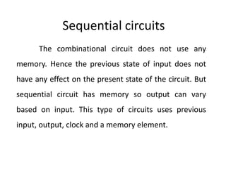
  • 1. Sequential circuits The combinational circuit does not use any memory. Hence the previous state of input does not have any effect on the present state of the circuit. But sequential circuit has memory so output can vary based on input. This type of circuits uses previous input, output, clock and a memory element.
  • 3. • Flip Flop • Flip flop is a sequential circuit which generally samples its inputs and changes its outputs only at particular instants of time and not continuously. Flip flop is said to be edge sensitive or edge triggered rather than being level triggered like latches.
  • 4. The NAND Gate SR Flip-Flop • The simplest way to make any basic single bit set- reset SR flip-flop is to connect together a pair of cross-coupled 2-input NAND gates as shown • To form a Set-Reset Bistable also known as an active LOW SR NAND Gate Latch, so that there is feedback from each output to one of the other NAND gate inputs. • This device consists of two inputs, one called the Set, S and the other called the Reset, R with two corresponding outputs Q and its inverse or complement Q (not-Q) as shown below.
  • 5. • Truth Table for this Set-Reset Function • State S R Q Q’ Description • Set 1 0 0 1 set Q’ » 1 1 1 0 1 no change • Reset 0 1 1 0 reset Q’ » 0 1 1 1 0 no change • Invalid 0 0 1 1 Invalid Condition
  • 6. • Clocked or Enabled S-R Flip Flop • It is basically S-R latch using NAND gates with an additional enable input. • It is also called as level triggered SR-FF. For this, circuit in output will take place if and only if the enable input (E) is made active. • In short this circuit will operate as an S-R latch if E = 1 but there is no change in the output if E = 0.
  • 9. Operation • Condition Operation S = R = 0 : No change If S = R = 0 then output of NAND gates 3 and 4 are forced to become 1. • Hence R' and S' both will be equal to 1. Since S' and R' are the input of the basic S-R latch using NAND gates, there will be no change in the state of outputs. • S = 0, R = 1, E = 1 Since S = 0, output of NAND-3 i.e. R' = 1 and E = 1 the output of NAND-4 i.e. S' = 0. • Hence Qn+1 = 0 and Qn+1 bar = 1. This is reset condition.
  • 10. • S = 1, R = 0, E = 1 Output of NAND-3 i.e. R' = 0 and output of NAND-4 i.e. S' = 1. • Hence output of S-R NAND latch is Qn+1 = 1 and Qn+1 bar = 0. This is the reset condition. • S = 1, R = 1, E = 1 As S = 1, R = 1 and E = 1, the output of NAND gates 3 and 4 both are 0 i.e. S' = R' = 0. • Hence the Race condition will occur in the basic NAND latch.
  • 11. JK Flip flop A JK flip-flop has two inputs similar to that of RS flip-flop. We can say JK flip-flop is a refinement of RS flip-flop. JK means Jack Kilby, a Texas instrument engineer who invented IC. The two inputs of JK Flip-flop is J (set) and K (reset). A JK flip-flop is nothing but a RS flip-flop along with two AND gates which are augmented to it.
  • 12. • The flip-flop is constructed in such a way that the output Q is ANDed with K and CP. • This arrangement is made so that the flip-flop is cleared during a clock pulse only if Q was previously 1. • Similarly Q’ is ANDed with J and CP, so that the flip-flop is cleared during a clock pulse only if Q’ was previously 1.
  • 13.
  • 14. Master Slave JK Flip Flop • Master slave JK FF is a cascade of two S-R FF with feedback from the output of second to input of first. • Master is a positive level triggered. But due to the presence of the inverter in the clock line, the slave will respond to the negative level. • Hence when the clock = 1 (positive level) the master is active and the slave is inactive. • Whereas when clock = 0 (low level) the slave is active and master is inactive.
  • 15. Circuit Diagram & Truthtable
  • 16. Operation • J = K = 0 (No change) When clock = 0, the slave becomes active and master is inactive. But since the S and R inputs have not changed, the slave outputs will also remain unchanged. Therefore outputs will not change if J = K =0. • J = 0 and K = 1 (Reset) Clock = 1 − Master active, slave inactive. Therefore outputs of the master become Q1 = 0 and Q1 bar = 1. That means S = 0 and R =1. • Clock = 0 − Slave active, master inactive. Therefore outputs of the slave become Q = 0 and Q bar = 1. • Again clock = 1 − Master active, slave inactive. Therefore even with the changed outputs Q = 0 and Q bar = 1 fed back to master, its output will be Q1 = 0 and Q1 bar = 1. That means S = 0 and R = 1. • Hence with clock = 0 and slave becoming active the outputs of slave will remain Q = 0 and Q bar = 1. Thus we get a stable output from the Master slave.
  • 17. • J = 1 and K = 0 (Set) Clock = 1 − Master active, slave inactive. Therefore outputs of the master become Q1 = 1 and Q1 bar = 0. That means S = 1 and R =0. • Clock = 0 − Slave active, master inactive. Therefore outputs of the slave become Q = 1 and Q bar = 0. • Again clock = 1 − then it can be shown that the outputs of the slave are stabilized to Q = 1 and Q bar = 0. • J = K = 1 (Toggle) Clock = 1 − Master active, slave inactive. Outputs of master will toggle. So S and R also will be inverted. • Clock = 0 − Slave active, master inactive. Outputs of slave will toggle. • These changed output are returned back to the master inputs. But since clock = 0, the master is still inactive. So it does not respond to these changed outputs. This avoids the multiple toggling which leads to the race around condition. The master slave flip flop will avoid the race around condition.
  • 18. Delay Flip Flop / D Flip Flop • Delay Flip Flop or D Flip Flop is the simple gated S-R latch with a NAND inverter connected between S and R inputs. • It has only one input. The input data is appearing at the output after some time. Due to this data delay between i/p and o/p, it is called delay flip flop. • S and R will be the complements of each other due to NAND inverter. Hence S = R = 0 or S = R = 1, these input condition will never appear. • This problem is avoid by SR = 00 and SR = 1 conditions.
  • 20. Operation • 1 E = 0 Latch is disabled. Hence no change in output. • 2 E = 1 and D = 0 If E = 1 and D = 0 then S = 0 and R = 1. Hence irrespective of the present state, the next state is Qn+1 = 0 and Qn+1 bar = 1. This is the reset condition. • 3 E = 1 and D = 1 If E = 1 and D = 1, then S = 1 and R = 0. This will set the latch and Qn+1 = 1 and Qn+1 bar = 0 irrespective of the present state.
  • 21. Toggle Flip Flop / T Flip Flop • Toggle flip flop is basically a JK flip flop with J and K terminals permanently connected together. • It has only input denoted by T as shown in the Symbol Diagram. The symbol for positive edge triggered T flip flop is shown in the Block Diagram.
  • 23. • Operation • T = 0, J = K = 0 The output Q and Q bar won't change. • T = 1, J = K = 1 Output will toggle corresponding to every leading edge of clock signal.