Downloaded 1,146 times

![STICK DIAGRAMS
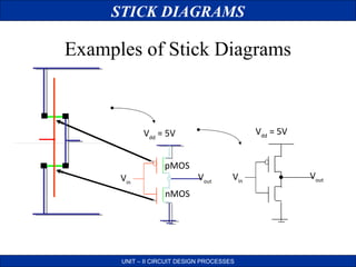
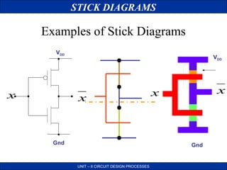
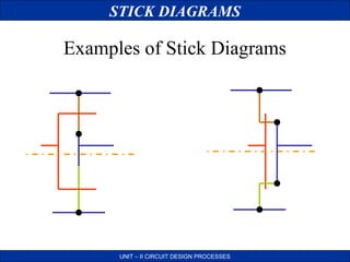
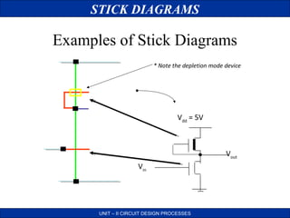
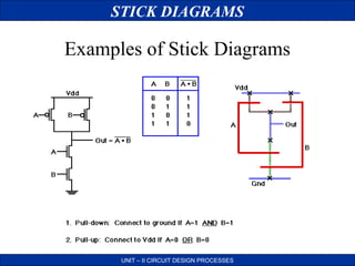
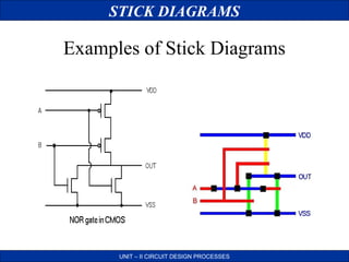
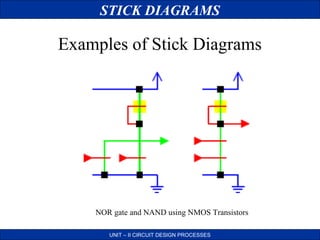
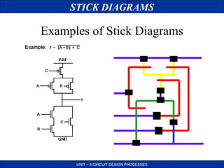
Examples of Stick Diagrams
f= [(xy) +z]’ using NMOS Transistors
UNIT – II CIRCUIT DESIGN PROCESSES](https://image.slidesharecdn.com/vlsicircuitdesignprocess-131101061939-phpapp01/85/VLSI-circuit-design-process-22-320.jpg)

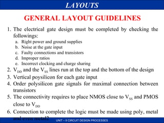


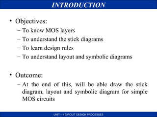
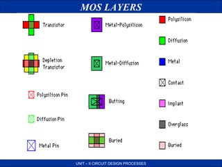
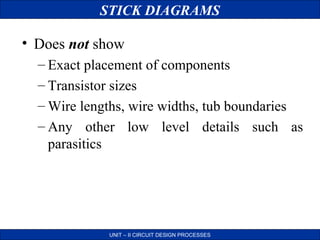
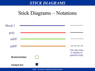
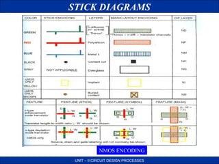
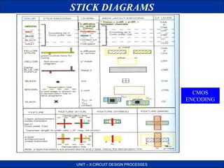
The document discusses circuit design processes and stick diagrams. It begins by introducing MOS layers and objectives of understanding stick diagrams, design rules, and layout. It then covers stick diagrams in depth, explaining that they show relative component placement and layer information through color codes as an interface between symbolic circuits and layouts. Examples of stick diagram rules, notations, and common MOS circuits are provided. Finally, it discusses design rules, explaining that they define feature sizes and spacings to interface between circuits and fabrication processes while allowing for manufacturing tolerances.