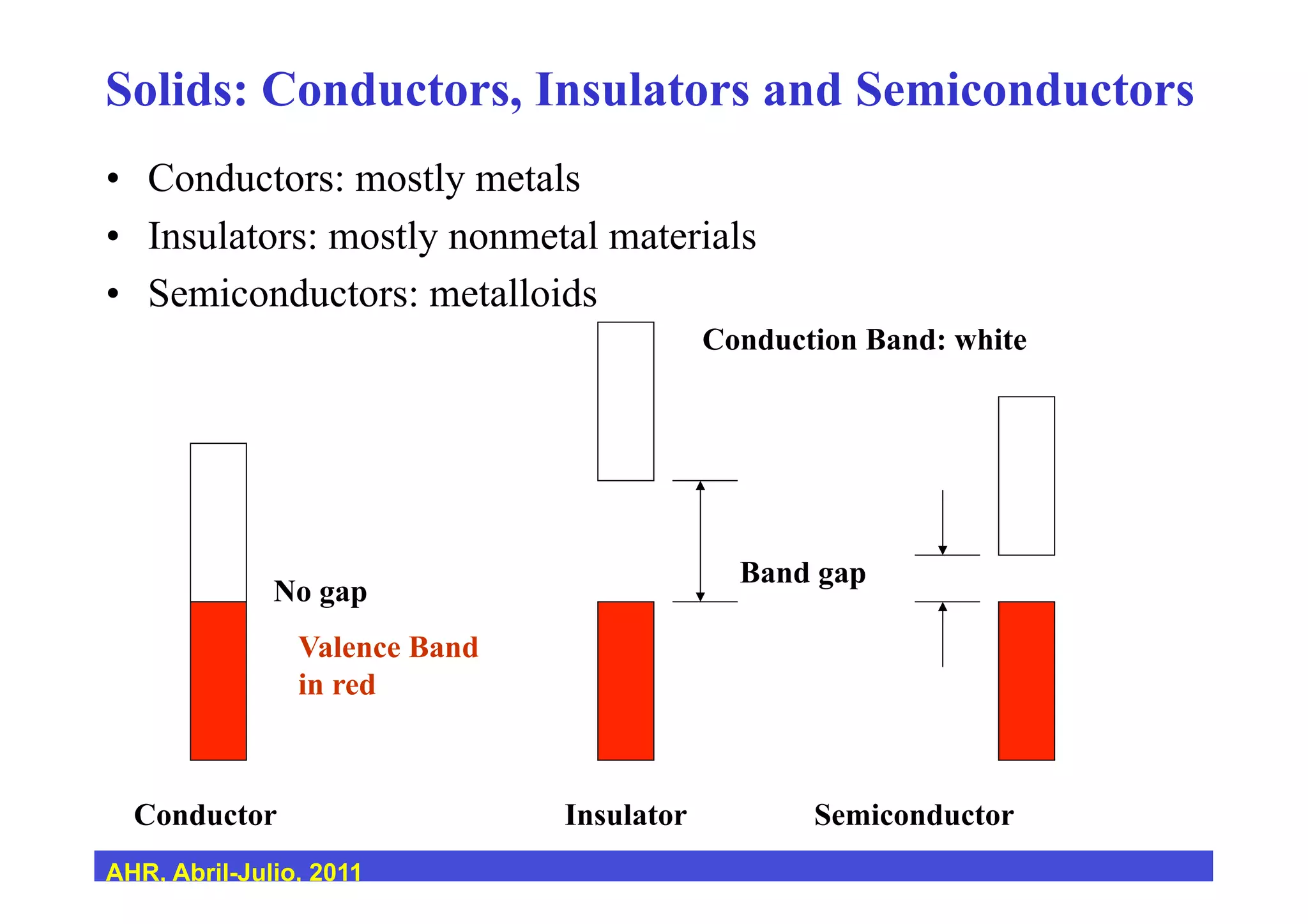
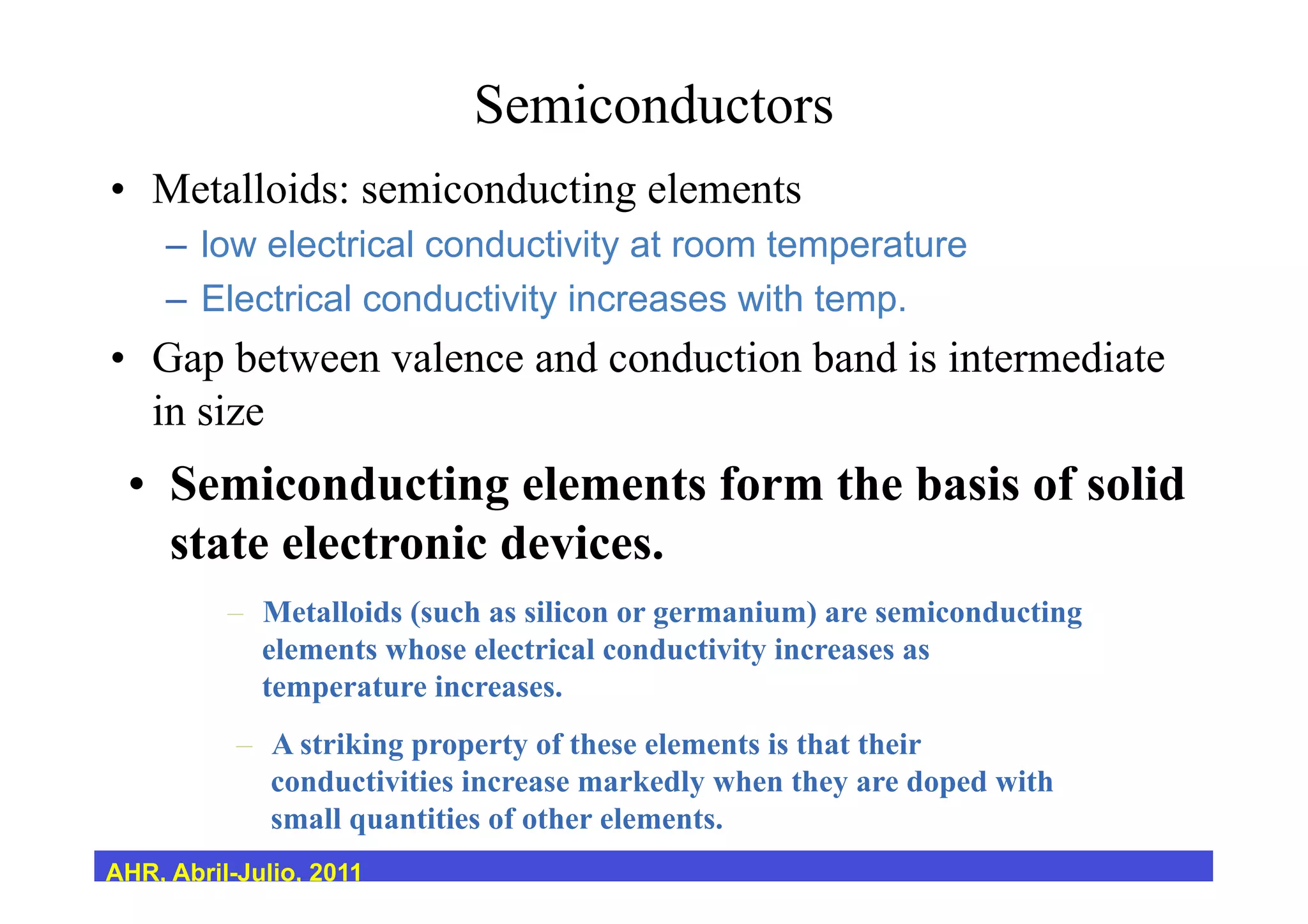
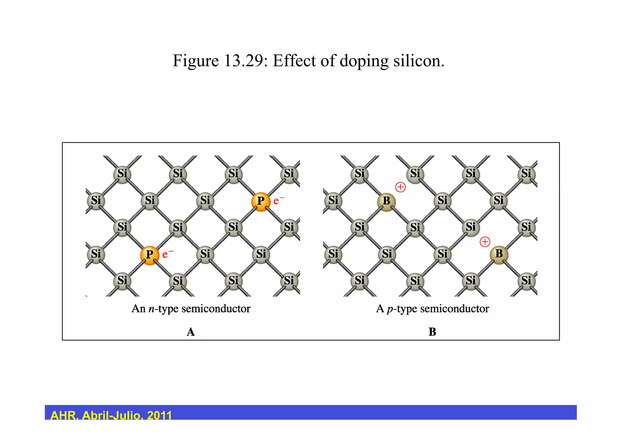
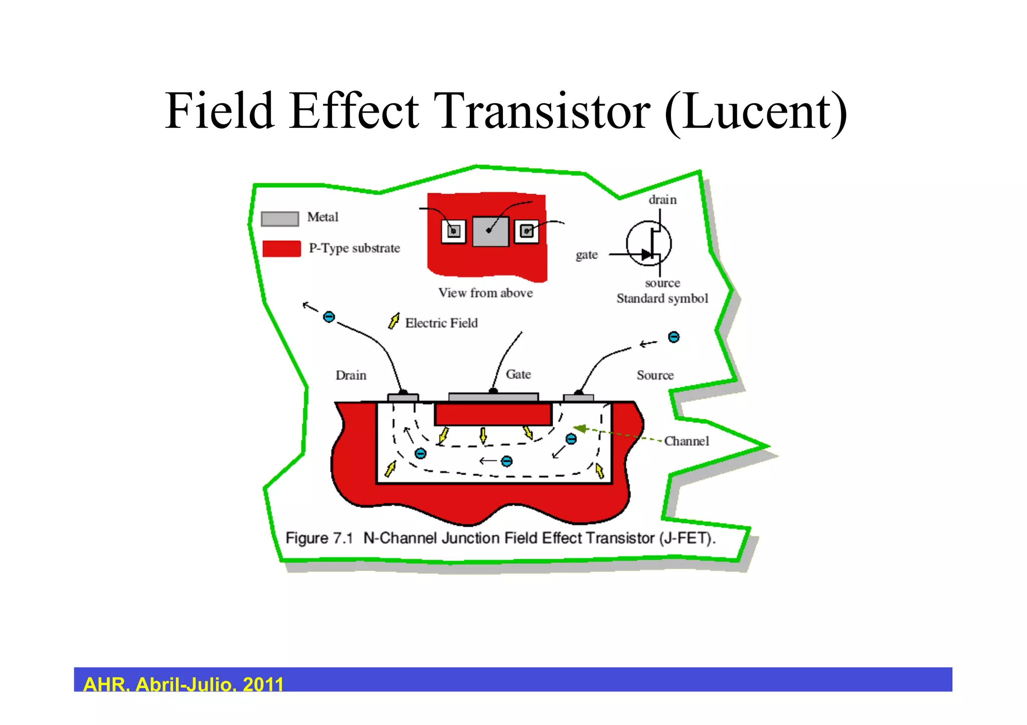
Solids: Conductors, Insulators and Semiconductors
•  Conductors: mostly metals
•  Insulators: mostly nonmetal materials
•  Semiconductors: metalloids
AHR, Abril-Julio, 2011
Conductor Insulator Semiconductor
Valence Band
in red
Conduction Band: white
Band gap
No gap
Sodium According to Band Theory
Conduction band:
empty 3s antibonding
Valence band:
full 3s bonding
No gap
AHR, Abril-Julio, 2011
Semiconductors
•  Metalloids: semiconducting elements
–  low electrical conductivity at room temperature
–  Electrical conductivity increases with temp.
•  Gap between valence and conduction band is intermediate
in size
•  Semiconducting elements form the basis of solid
state electronic devices.
–  Metalloids (such as silicon or germanium) are semiconducting
elements whose electrical conductivity increases as
temperature increases.
–  A striking property of these elements is that their
conductivities increase markedly when they are doped with
small quantities of other elements.
AHR, Abril-Julio, 2011
Semiconductors
•  Semiconducting elements form the basis of solid
state electronic devices.
–  When silicon is doped with phosphorus, it becomes an n-
type semiconductor, in which electric current is carried by
electrons.
–  When silicon is doped with boron, it becomes a p-type
semiconductor, in which an electrical current is
carried by positively charged holes
–  Joining a p-type semiconductor to an n-type
semiconductor produces a p-n junction, which can
function as a rectifier.
–  A rectifier is a device that allows current to flow in
one direction, but not the other.
AHR, Abril-Julio, 2011
Figure 13.29: Effect of doping silicon.
AHR, Abril-Julio, 2011
7
A p-n junction as a
rectifier.
AHR, Abril-Julio, 2011
SEMICONDUCTORS
•  Made from materials that have four valence electrons in
their outer orbits
•  Germanium and silicon are the most common
semiconductor materials used in solid-state devices
•  Silicon is preferred due to its ability to withstand heat
•  When refined into a pure form, the molecules arrange
themselves into a structure called a lattice structure
•  A pure semiconductor material such as silicon or
germanium has no special properties and will make a poor
conductive material.
AHR, Abril-Julio, 2011
•  To make semiconductor material useful for solid-state
components, it is doped with an impurity
•  This impurity could be indium or gallium, both of which
have only three valence (trivalent) electrons
•  With the doping of impurity, the lattice structure changes,
leaving a hole in the material where an electron could
reside.
•  Since it now lacks an electron, the material is no longer
electrically neutral, it now carries a net positive charge…
hence P-type material.
•  In a P-type material, designate the holes as the majority
carriers, and electrons the minority carriers
P-type MATERIAL
AHR, Abril-Julio, 2011
P-type MATERIAL
Lattice structure of a P-type material
AHR, Abril-Julio, 2011
•  Is made by doping semiconductor material with an
impurity that has five valence (pentavalent) electrons
such as arsenic or antimony
•  Now the lattice structure has an excess of electrons,
and a net negative charge… hence N-type material
•  These excessive electrons will enable free electron
movement under certain conditions, much like a
conductor.
•  In an N-type material, they designate the electrons
as the major carriers, and holes as the minority
carriers
N-type MATERIAL
AHR, Abril-Julio, 2011
N-type MATERIAL
Lattice structure of a N-type material
AHR, Abril-Julio, 2011
•  All solid-state devices are made from a combination
of P and N-type materials
•  The type of device formed is determined by how the
P and N-type materials are connected; the number of
layers; and thickness of layers
•  Examples:
SOLID-STATE DEVICES
The PN junction or
diode
The
transistor
AHR, Abril-Julio, 2011
•  In the nineteenth century, scientists were rarely
inventors: Samuel F.B. Morse, Alexander Graham
Bell, Thomas Alva Edison
•  In the twentieth century, scientists invaded the
domain of invention: John Fleming invented the
vacuum diode tube and Lee De Forest invented the
triode tube
•  The transistor can be viewed, as can the laser, as an
invention of physicists.
–  Source: Bunch and Hellemans, The Timetables of Technology,
Simon and Schuster, 1993
AHR, Abril-Julio, 2011
William B. Shockley (1910-1989)
•  Known as the Father of the Transistor
•  joined Bell Labs in 1936 in the vacuum tube
department (solid state physicist)
•  Moved to the semiconductor laboratory:
–  It has today occurred to me that an amplifier using
semiconductors rather than vacuum tubes is in principle
possible.
AHR, Abril-Julio, 2011
Walter Houser Brattain
•  Experimental physicist who also worked on vacuum
tubes
•  Joined Shockley and Bardeen in semiconductor
research.
AHR, Abril-Julio, 2011
John Bardeen (1908-1991)
•  Physicist, Naval Ordnance Laboratory 1941-1945
•  Research Physicist, Bell Telephone Laboratories 1945-1951 (theorist)
•  Professor of Electrical Engineering,
–  University of Illinois, 1951-1978
•  Nobel Prize in Physics: 1956 and 1972
•  transistor (1956) and superconductivity (1972)
–  I knew the transistor was important, but I never foresaw the
revolution in electronics it would bring.
AHR, Abril-Julio, 2011
Nobel Prize in 1956
•  Shockley, Brattain and Bardeen start
working with p- and n- type germanium
and silicon semiconductors in 1946
•  Bardeen and Brattain put together the
first transistor in December 1947:
–  a point-contact transistor consisting of a
single germanium crystal with a p- and an
n- zone. Two wires made contact with the
crystal near the junction between the two
zones like the whiskers of a crystal-
radio set.
AHR, Abril-Julio, 2011
•  Shockley immediately set out to define the effects that they
had observed, i.e., to explain the physics of transistors
•  A few months later, Shockley devised the junction
transistor, a true solid-state device which did not need the
whiskers of the point-contact transistor.
•  AT&T licensed the transistor very cheaply to other
manufacturers and waived patent rights for the use of
transistors in hearing aids, in the spirit of its founder,
Alexander Graham Bell
Shockley s sandwich
transistor
AHR, Abril-Julio, 2011
Manufacturing transistors on a chip
•  Shockley Semiconductor Laboratories,
Palo Alto, CA (1954)
–  the beginnings of Silicon Valley
•  Fairchild Semiconductors founded in Mountain
View, CA (1957) by eight Shockley employees
including Gordon Moore and Robert Noyce
•  Bell Labs had made several improvements in the
manufacturing of crystals of silicon and germanium
with the impurities needed to create semiconductors
AHR, Abril-Julio, 2011
Meanwhile….
•  Jack Kilby worked for Texas Instruments
•  Conceived of a manufacturing method that
allowed the miniaturization of electronic circuits
on semiconductor chips, called integrated circuits
or ICs.
•  Kilby had reduced the transistor to the size of a
match head
•  Texas Instruments sold these for $450.
AHR, Abril-Julio, 2011
And at Fairchild….
•  Noyce adapted a system called planar
manufacturing, in which all the transistors and
resistors were formed together on a silicon chip
with the metal wiring embedded in the silicon.
•  Noyce filed for a patent five months after TI
•  Lawsuit: TI claimed patent infringement; TI lost
but companies needed licenses from both
companies.
–  source: Shurkin, Engines of the Mind, 1984
AHR, Abril-Julio, 2011
Field Effect Transistor (Lucent)
AHR, Abril-Julio, 2011
•  Due to improvements in manufacturing, integrated
circuits became smaller and smaller
•  Gordon Moore observed that the number of
transistors on a chip seems to double every year….
–  Moore s Law: the number of transistors on a chip seems
to double every 18 months, while the price remains the
same.
–  Grosch s law for mainframes: every year, the power of
computers doubles while the price is cut in half
AHR, Abril-Julio, 2011
A Little Economic Sociology
•  No matter how rich you are working for
someone else, think of how rich you could be
if you worked for yourself!
•  People figured out quickly that one could bolt
from one company, and with enough science,
engineering and venture capital start a new
company down the street.
•  Silicon Valley grew and grew and grew!
–  source: Shurkin, Engines of the Mind, 1984
AHR, Abril-Julio, 2011
Bergin s musings….
•  The greatest deterrent to success is success!
•  Large companies tend to be conservative and
bureaucratic with lengthy approval processes which
stifle new ideas.
•  Small companies have no history, they need to take
risks and they have no stockholders to answer to:
Apple, Osborne, etc.
•  Starting technology companies became the new
gold rush (and it was in California!)
AHR, Abril-Julio, 2011
Intel
•  Noyce, Moore, and Andrew Grove leave Fairchild
and found Intel in 1968
–  focus on random access memory (RAM) chips
•  Question: if you can put transistors, capacitors,
etc. on a chip, why couldn t you put a central
processor on a chip?
•  Ted Hoff designs the Intel 4004, the first
microprocessor in 1969
–  based on Digital s PDP-8
AHR, Abril-Julio, 2011
Microcomputers
•  Ed Roberts founds Micro Instrumentation Telemetry
Systems (MITS) in 1968
•  Popular Electronics puts the MITS Altair on the
cover in January 1975 [nee PE-8, Intel 8080]
•  Les Solomon s 12 year old daughter, Lauren, was a
lover of Star Trek. He asked her what the name of
the computer on the Enterprise was. She said
computer but why don t you call it Altair because
that is where they are going tonight!
AHR, Abril-Julio, 2011
Altair 8800 Computer
Intel processors
•  CPU Year Data Memory MIPS
•  4004 1971 4 1K
•  8008 1972 8 16K
•  8080 1974 8 64K
•  8088 1980 8 1M .33
•  80286 1982 16 1M 3
•  80386 1985 32 4G 11
•  80486 1989 32 4G 41
•  Pentium 1993 64 4G 111
Inter-band absorption (direct gap)
Finite amount of electrons results in filled and empty states
In semiconductor, highest-energy filled states are in the valence band
Lowest unoccupied states are in the conduction band
E
k0 π/a 2π/a 3π/aa -2π/a -π/a
valence electrons
conduction electrons
filled
empty
Egap
Energy difference between valence and conduction band
is called the bandgap of the semiconductor
Material is called a semiconductor if Egap < 4eV, and insulator if Egap > 4eV
AHR, Abril-Julio, 2011
Energy levels in real semiconductors
In three dimensions, the dispersion relation depends on direction in the
crystal
source: Optical
Properties of
Semiconductor
Nanocrystals,
Gaponenko
AHR, Abril-Julio, 2011
Single atoms are surrounded by bound electrons
In solids: electrons in neighboring atoms can interact:
⇒ electron levels are modified, resulting in energy bands
In semiconductors the highest-energy band that is filled (occupied by electrons)
is the valence band, and the lowest unoccupied states are in the conduction band
strongest optical response if electron transitions can be induced
E
k0 π/a 2π/a 3π/a-2π/a -π/a
filled
empty
Egap valence
states
(usually filled)
conduction
states
(usually empty)
E
k
E
k
AHR, Abril-Julio, 2011
Direct-gap semiconductor: highest occupied and lowest unoccupied state occur at
k=0
Light can induce electronic transitions if
energy and momentum are conserved:
Efinal – Einitial = Ephot and Δk = ≈ 0
(Photon: long wavelength compared
to atomic spacing ⇒ kphot « π/a )
photk
E
k
Direct gap semiconductors
Photons with E < Egap have insufficient energy to kick a valence
electron into a conduction state ⇒ absorption starts at Ephot =
Egap
These band-band absorptions have the usual implications for n and κ
(recall Kramers-Kronig relations)
AHR, Abril-Julio, 2011
Indirect-gap semiconductor: highest occupied and lowest unoccupied state have
Δk≠0
Direct transitions possible for Δk≈0
⇒ strong direct interband absorption
occurs at E > Egap
Other possibility: momentum and
energy can be conserved by photon
absorption and simultaneous absorption or
emission of a phonon:
Indirect transitions possible with
assistance of a phonon
Shown here are optically induced transitions
- during phonon emission
a phonon is generated in the process
- during phonon absorption
a phonon is generated in the process
Egap
Egap
AHR, Abril-Julio, 2011
Excitons
Excitons are combined electron-hole states:
A free electron and a free hole (empty electronic state in the valence band)
exert Coulomb force on each other:
hydrogen-like bound states possible: excitonic states
e
h
Coulomb
force
n=3
n=2
n=1
E
k
Eb
Wave functions of electron and hole look similar to free electron and free hole
Note: exciton can move through crystal, i.e. not bound to specific atom!
Eb is the exciton
binding energy =
energy released upon
exciton formation, or
energy required for
exciton breakup
AHR, Abril-Julio, 2011
Excitonic absorption
Light can excite an electron from the valence band and generate an exciton
at energies slightly below the bandgap
⇒ see absorption at Ephot = Egap – Eb (absorption slightly below Egap)
Exciton binding energy on the order of a few meV
Thermal energy at room temperature: kT ~ 25 meV
⇒ exciton rapidly dissociates at room temperature
⇒ absorption lines broaden / disappear for higher temperatures
e
h
Coulomb
force
n=3
n=2
n=1
E
k
Eb
AHR, Abril-Julio, 2011
Optical transitions related to dopant atoms
Ga: 3 valence electrons
Si: 4 valence electrons
As: 5 valence electrons
AHR, Abril-Julio, 2011
Donor levels
Substitute Si atom with As atom (impurity atom in the Si lattice):
weakly bound extra valence electron
Low T: donors neutral, electron weakly bound
lew energy light can excite donor electron in to conduciton
band
Binding energy Ed similar to kT at room temperature
( RT ):
At room temperature the bound electron is quickly released
⇒ impurity mostly ionized at RT : Arsenic is a donor in Si
At RT such transitions are typically too broad to observe
Low T
RT
AHR, Abril-Julio, 2011
Acceptor levels
Substitute Si atom with Ga atom : empty electronic state just above the Si
valence band: at finite temperature, Si valence electron may fill acceptor level
⇒ location of unoccupied valence state (hole) can orbit the charged Ga dopant
Binding energy Ea similar to kT at room temperature ( RT ):
At room temperature the hole can leave the dopant,
producing a free charge
‘hole’ =
available
electron
state
AHR, Abril-Julio, 2011
Infrared absorption due to dopants
Dopant binding energies low: donor level related absorptions invisible at RT,
but observable at low temperatures
Example: direct valence band → acceptor level absorption in boron doped Si
Transition at ~40 meV ⇒ absorption at λ≈30 µm : infrared
AHR, Abril-Julio, 2011
Dopant related transitions
Possible dopant related transitions:
Typically visible at low T, but not clearly observable at RT
AHR, Abril-Julio, 2011
Free carrier absorption (1/2)
At RT, predominant dopant related absorption is free carrier absorption
in which a photon excites an electron into a higher lying state
Example: p-type semiconductors: filled states in the conduction band:
optical transitions possible at Ephot < Egap !
Free electrons:
absorption typically indirect
phonon-assisted transition
Free holes can make direct transitions
form the heavy-hole band
to the light-hole band
⇒ holes cause stronger free carrier
absorption than electrons
AHR, Abril-Julio, 2011
Free carrier absorption (2/2)
Free electron absorption can be described by the Drude model
Dopant levels in semiconductors range from ~1014 - 1018 /cm3
which is ~108 – 106 lower than free electron densities in metals
Plasma frequency of doped semiconductors 104 - 103 lower than of metals: IR
3
2
3
2
2
2
)(",1)('
ω
ω
τω
ω
ωε
ω
ω
ωε
Γ
=≈−≈
pp
r
p
r
2
2
2
2
)(")(
p
p
ccc λ
λ
ω
ω
ωε
ω
ωα
Γ
=
Γ
≅≅
At frequencies above plasma frequency,εr and α described by
Electron FCA up for lower energies
Free hole absorption less well defined
AHR, Abril-Julio, 2011
Band to band transition
AHR, Abril-Julio, 2011
Direct vs indirect gaps
AHR, Abril-Julio, 2011

Solids, Conductors, Insulators & Semiconductors

  • 1.
    Solids: Conductors, Insulatorsand Semiconductors •  Conductors: mostly metals •  Insulators: mostly nonmetal materials •  Semiconductors: metalloids AHR, Abril-Julio, 2011 Conductor Insulator Semiconductor Valence Band in red Conduction Band: white Band gap No gap
  • 2.
    Sodium According toBand Theory Conduction band: empty 3s antibonding Valence band: full 3s bonding No gap AHR, Abril-Julio, 2011
  • 3.
    Semiconductors •  Metalloids: semiconductingelements –  low electrical conductivity at room temperature –  Electrical conductivity increases with temp. •  Gap between valence and conduction band is intermediate in size •  Semiconducting elements form the basis of solid state electronic devices. –  Metalloids (such as silicon or germanium) are semiconducting elements whose electrical conductivity increases as temperature increases. –  A striking property of these elements is that their conductivities increase markedly when they are doped with small quantities of other elements. AHR, Abril-Julio, 2011
  • 4.
    Semiconductors •  Semiconducting elementsform the basis of solid state electronic devices. –  When silicon is doped with phosphorus, it becomes an n- type semiconductor, in which electric current is carried by electrons. –  When silicon is doped with boron, it becomes a p-type semiconductor, in which an electrical current is carried by positively charged holes –  Joining a p-type semiconductor to an n-type semiconductor produces a p-n junction, which can function as a rectifier. –  A rectifier is a device that allows current to flow in one direction, but not the other. AHR, Abril-Julio, 2011
  • 6.
    Figure 13.29: Effectof doping silicon. AHR, Abril-Julio, 2011
  • 7.
    7 A p-n junctionas a rectifier. AHR, Abril-Julio, 2011
  • 8.
    SEMICONDUCTORS •  Made frommaterials that have four valence electrons in their outer orbits •  Germanium and silicon are the most common semiconductor materials used in solid-state devices •  Silicon is preferred due to its ability to withstand heat •  When refined into a pure form, the molecules arrange themselves into a structure called a lattice structure •  A pure semiconductor material such as silicon or germanium has no special properties and will make a poor conductive material. AHR, Abril-Julio, 2011
  • 9.
    •  To makesemiconductor material useful for solid-state components, it is doped with an impurity •  This impurity could be indium or gallium, both of which have only three valence (trivalent) electrons •  With the doping of impurity, the lattice structure changes, leaving a hole in the material where an electron could reside. •  Since it now lacks an electron, the material is no longer electrically neutral, it now carries a net positive charge… hence P-type material. •  In a P-type material, designate the holes as the majority carriers, and electrons the minority carriers P-type MATERIAL AHR, Abril-Julio, 2011
  • 10.
    P-type MATERIAL Lattice structureof a P-type material AHR, Abril-Julio, 2011
  • 11.
    •  Is madeby doping semiconductor material with an impurity that has five valence (pentavalent) electrons such as arsenic or antimony •  Now the lattice structure has an excess of electrons, and a net negative charge… hence N-type material •  These excessive electrons will enable free electron movement under certain conditions, much like a conductor. •  In an N-type material, they designate the electrons as the major carriers, and holes as the minority carriers N-type MATERIAL AHR, Abril-Julio, 2011
  • 12.
    N-type MATERIAL Lattice structureof a N-type material AHR, Abril-Julio, 2011
  • 13.
    •  All solid-statedevices are made from a combination of P and N-type materials •  The type of device formed is determined by how the P and N-type materials are connected; the number of layers; and thickness of layers •  Examples: SOLID-STATE DEVICES The PN junction or diode The transistor AHR, Abril-Julio, 2011
  • 14.
    •  In thenineteenth century, scientists were rarely inventors: Samuel F.B. Morse, Alexander Graham Bell, Thomas Alva Edison •  In the twentieth century, scientists invaded the domain of invention: John Fleming invented the vacuum diode tube and Lee De Forest invented the triode tube •  The transistor can be viewed, as can the laser, as an invention of physicists. –  Source: Bunch and Hellemans, The Timetables of Technology, Simon and Schuster, 1993 AHR, Abril-Julio, 2011
  • 15.
    William B. Shockley(1910-1989) •  Known as the Father of the Transistor •  joined Bell Labs in 1936 in the vacuum tube department (solid state physicist) •  Moved to the semiconductor laboratory: –  It has today occurred to me that an amplifier using semiconductors rather than vacuum tubes is in principle possible. AHR, Abril-Julio, 2011
  • 16.
    Walter Houser Brattain • Experimental physicist who also worked on vacuum tubes •  Joined Shockley and Bardeen in semiconductor research. AHR, Abril-Julio, 2011
  • 17.
    John Bardeen (1908-1991) • Physicist, Naval Ordnance Laboratory 1941-1945 •  Research Physicist, Bell Telephone Laboratories 1945-1951 (theorist) •  Professor of Electrical Engineering, –  University of Illinois, 1951-1978 •  Nobel Prize in Physics: 1956 and 1972 •  transistor (1956) and superconductivity (1972) –  I knew the transistor was important, but I never foresaw the revolution in electronics it would bring. AHR, Abril-Julio, 2011
  • 18.
    Nobel Prize in1956 •  Shockley, Brattain and Bardeen start working with p- and n- type germanium and silicon semiconductors in 1946 •  Bardeen and Brattain put together the first transistor in December 1947: –  a point-contact transistor consisting of a single germanium crystal with a p- and an n- zone. Two wires made contact with the crystal near the junction between the two zones like the whiskers of a crystal- radio set. AHR, Abril-Julio, 2011
  • 19.
    •  Shockley immediatelyset out to define the effects that they had observed, i.e., to explain the physics of transistors •  A few months later, Shockley devised the junction transistor, a true solid-state device which did not need the whiskers of the point-contact transistor. •  AT&T licensed the transistor very cheaply to other manufacturers and waived patent rights for the use of transistors in hearing aids, in the spirit of its founder, Alexander Graham Bell Shockley s sandwich transistor AHR, Abril-Julio, 2011
  • 20.
    Manufacturing transistors ona chip •  Shockley Semiconductor Laboratories, Palo Alto, CA (1954) –  the beginnings of Silicon Valley •  Fairchild Semiconductors founded in Mountain View, CA (1957) by eight Shockley employees including Gordon Moore and Robert Noyce •  Bell Labs had made several improvements in the manufacturing of crystals of silicon and germanium with the impurities needed to create semiconductors AHR, Abril-Julio, 2011
  • 21.
    Meanwhile…. •  Jack Kilbyworked for Texas Instruments •  Conceived of a manufacturing method that allowed the miniaturization of electronic circuits on semiconductor chips, called integrated circuits or ICs. •  Kilby had reduced the transistor to the size of a match head •  Texas Instruments sold these for $450. AHR, Abril-Julio, 2011
  • 22.
    And at Fairchild…. • Noyce adapted a system called planar manufacturing, in which all the transistors and resistors were formed together on a silicon chip with the metal wiring embedded in the silicon. •  Noyce filed for a patent five months after TI •  Lawsuit: TI claimed patent infringement; TI lost but companies needed licenses from both companies. –  source: Shurkin, Engines of the Mind, 1984 AHR, Abril-Julio, 2011
  • 23.
    Field Effect Transistor(Lucent) AHR, Abril-Julio, 2011
  • 24.
    •  Due toimprovements in manufacturing, integrated circuits became smaller and smaller •  Gordon Moore observed that the number of transistors on a chip seems to double every year…. –  Moore s Law: the number of transistors on a chip seems to double every 18 months, while the price remains the same. –  Grosch s law for mainframes: every year, the power of computers doubles while the price is cut in half AHR, Abril-Julio, 2011
  • 25.
    A Little EconomicSociology •  No matter how rich you are working for someone else, think of how rich you could be if you worked for yourself! •  People figured out quickly that one could bolt from one company, and with enough science, engineering and venture capital start a new company down the street. •  Silicon Valley grew and grew and grew! –  source: Shurkin, Engines of the Mind, 1984 AHR, Abril-Julio, 2011
  • 26.
    Bergin s musings…. • The greatest deterrent to success is success! •  Large companies tend to be conservative and bureaucratic with lengthy approval processes which stifle new ideas. •  Small companies have no history, they need to take risks and they have no stockholders to answer to: Apple, Osborne, etc. •  Starting technology companies became the new gold rush (and it was in California!) AHR, Abril-Julio, 2011
  • 27.
    Intel •  Noyce, Moore,and Andrew Grove leave Fairchild and found Intel in 1968 –  focus on random access memory (RAM) chips •  Question: if you can put transistors, capacitors, etc. on a chip, why couldn t you put a central processor on a chip? •  Ted Hoff designs the Intel 4004, the first microprocessor in 1969 –  based on Digital s PDP-8 AHR, Abril-Julio, 2011
  • 28.
    Microcomputers •  Ed Robertsfounds Micro Instrumentation Telemetry Systems (MITS) in 1968 •  Popular Electronics puts the MITS Altair on the cover in January 1975 [nee PE-8, Intel 8080] •  Les Solomon s 12 year old daughter, Lauren, was a lover of Star Trek. He asked her what the name of the computer on the Enterprise was. She said computer but why don t you call it Altair because that is where they are going tonight! AHR, Abril-Julio, 2011
  • 29.
  • 30.
    Intel processors •  CPUYear Data Memory MIPS •  4004 1971 4 1K •  8008 1972 8 16K •  8080 1974 8 64K •  8088 1980 8 1M .33 •  80286 1982 16 1M 3 •  80386 1985 32 4G 11 •  80486 1989 32 4G 41 •  Pentium 1993 64 4G 111
  • 31.
    Inter-band absorption (directgap) Finite amount of electrons results in filled and empty states In semiconductor, highest-energy filled states are in the valence band Lowest unoccupied states are in the conduction band E k0 π/a 2π/a 3π/aa -2π/a -π/a valence electrons conduction electrons filled empty Egap Energy difference between valence and conduction band is called the bandgap of the semiconductor Material is called a semiconductor if Egap < 4eV, and insulator if Egap > 4eV AHR, Abril-Julio, 2011
  • 32.
    Energy levels inreal semiconductors In three dimensions, the dispersion relation depends on direction in the crystal source: Optical Properties of Semiconductor Nanocrystals, Gaponenko AHR, Abril-Julio, 2011
  • 33.
    Single atoms aresurrounded by bound electrons In solids: electrons in neighboring atoms can interact: ⇒ electron levels are modified, resulting in energy bands In semiconductors the highest-energy band that is filled (occupied by electrons) is the valence band, and the lowest unoccupied states are in the conduction band strongest optical response if electron transitions can be induced E k0 π/a 2π/a 3π/a-2π/a -π/a filled empty Egap valence states (usually filled) conduction states (usually empty) E k E k AHR, Abril-Julio, 2011
  • 34.
    Direct-gap semiconductor: highestoccupied and lowest unoccupied state occur at k=0 Light can induce electronic transitions if energy and momentum are conserved: Efinal – Einitial = Ephot and Δk = ≈ 0 (Photon: long wavelength compared to atomic spacing ⇒ kphot « π/a ) photk E k Direct gap semiconductors Photons with E < Egap have insufficient energy to kick a valence electron into a conduction state ⇒ absorption starts at Ephot = Egap These band-band absorptions have the usual implications for n and κ (recall Kramers-Kronig relations) AHR, Abril-Julio, 2011
  • 35.
    Indirect-gap semiconductor: highestoccupied and lowest unoccupied state have Δk≠0 Direct transitions possible for Δk≈0 ⇒ strong direct interband absorption occurs at E > Egap Other possibility: momentum and energy can be conserved by photon absorption and simultaneous absorption or emission of a phonon: Indirect transitions possible with assistance of a phonon Shown here are optically induced transitions - during phonon emission a phonon is generated in the process - during phonon absorption a phonon is generated in the process Egap Egap AHR, Abril-Julio, 2011
  • 36.
    Excitons Excitons are combinedelectron-hole states: A free electron and a free hole (empty electronic state in the valence band) exert Coulomb force on each other: hydrogen-like bound states possible: excitonic states e h Coulomb force n=3 n=2 n=1 E k Eb Wave functions of electron and hole look similar to free electron and free hole Note: exciton can move through crystal, i.e. not bound to specific atom! Eb is the exciton binding energy = energy released upon exciton formation, or energy required for exciton breakup AHR, Abril-Julio, 2011
  • 37.
    Excitonic absorption Light canexcite an electron from the valence band and generate an exciton at energies slightly below the bandgap ⇒ see absorption at Ephot = Egap – Eb (absorption slightly below Egap) Exciton binding energy on the order of a few meV Thermal energy at room temperature: kT ~ 25 meV ⇒ exciton rapidly dissociates at room temperature ⇒ absorption lines broaden / disappear for higher temperatures e h Coulomb force n=3 n=2 n=1 E k Eb AHR, Abril-Julio, 2011
  • 38.
    Optical transitions relatedto dopant atoms Ga: 3 valence electrons Si: 4 valence electrons As: 5 valence electrons AHR, Abril-Julio, 2011
  • 39.
    Donor levels Substitute Siatom with As atom (impurity atom in the Si lattice): weakly bound extra valence electron Low T: donors neutral, electron weakly bound lew energy light can excite donor electron in to conduciton band Binding energy Ed similar to kT at room temperature ( RT ): At room temperature the bound electron is quickly released ⇒ impurity mostly ionized at RT : Arsenic is a donor in Si At RT such transitions are typically too broad to observe Low T RT AHR, Abril-Julio, 2011
  • 40.
    Acceptor levels Substitute Siatom with Ga atom : empty electronic state just above the Si valence band: at finite temperature, Si valence electron may fill acceptor level ⇒ location of unoccupied valence state (hole) can orbit the charged Ga dopant Binding energy Ea similar to kT at room temperature ( RT ): At room temperature the hole can leave the dopant, producing a free charge ‘hole’ = available electron state AHR, Abril-Julio, 2011
  • 41.
    Infrared absorption dueto dopants Dopant binding energies low: donor level related absorptions invisible at RT, but observable at low temperatures Example: direct valence band → acceptor level absorption in boron doped Si Transition at ~40 meV ⇒ absorption at λ≈30 µm : infrared AHR, Abril-Julio, 2011
  • 42.
    Dopant related transitions Possibledopant related transitions: Typically visible at low T, but not clearly observable at RT AHR, Abril-Julio, 2011
  • 43.
    Free carrier absorption(1/2) At RT, predominant dopant related absorption is free carrier absorption in which a photon excites an electron into a higher lying state Example: p-type semiconductors: filled states in the conduction band: optical transitions possible at Ephot < Egap ! Free electrons: absorption typically indirect phonon-assisted transition Free holes can make direct transitions form the heavy-hole band to the light-hole band ⇒ holes cause stronger free carrier absorption than electrons AHR, Abril-Julio, 2011
  • 44.
    Free carrier absorption(2/2) Free electron absorption can be described by the Drude model Dopant levels in semiconductors range from ~1014 - 1018 /cm3 which is ~108 – 106 lower than free electron densities in metals Plasma frequency of doped semiconductors 104 - 103 lower than of metals: IR 3 2 3 2 2 2 )(",1)(' ω ω τω ω ωε ω ω ωε Γ =≈−≈ pp r p r 2 2 2 2 )(")( p p ccc λ λ ω ω ωε ω ωα Γ = Γ ≅≅ At frequencies above plasma frequency,εr and α described by Electron FCA up for lower energies Free hole absorption less well defined AHR, Abril-Julio, 2011
  • 45.
    Band to bandtransition AHR, Abril-Julio, 2011
  • 46.
    Direct vs indirectgaps AHR, Abril-Julio, 2011