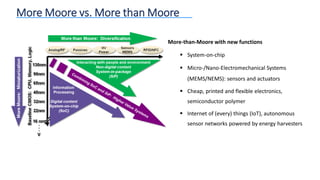
The document outlines the scope and topics covered in a course on advanced semiconductor devices. The course will consist of 12 lectures covering topics such as CMOS technology, advanced silicon devices, compound semiconductors, novel device platforms, and sensors and actuators. It will provide an introduction to semiconductor history and trends, as well as overview key fabrication techniques and characterization methods. The exam will be an oral exam where students can use their printed lecture notes.
This document provides information about the EC303 CMOS VLSI Design course at the National Institute of Technology Warangal. The course aims to teach students about MOSFET fabrication, CMOS inverter analysis and design, digital and analog circuit design using CMOS gates, and trends in CMOS technology. The syllabus covers topics such as MOSFET characteristics, inverters, digital circuits using techniques like pseudo NMOS and domino logic, analog circuits including amplifiers, and emerging technologies like FinFETs. Reading materials including textbooks on digital and analog CMOS IC design are also listed.
The document summarizes the history and evolution of semiconductor transistors from their inception to modern FinFET and GAA technologies. It traces transistors from early patents in the 1920s-1930s to the first working transistor in 1947. Key developments include the switch to silicon in the 1950s, the MOSFET in 1959, and planar processing techniques in the 1960s which led to MOSFET dominance by the 1970s. The document then discusses post-scaling innovations like strained silicon and high-k dielectrics in the 2000s. It introduces FinFETs which addressed short channel effects below 28nm with 3D tri-gate structures starting in 2007. Future technologies discussed include GAA which provides full gate control with nano-sheets to
This document provides a history of the MOSFET from its origins in the 1930s patents by Heil and Lilienfeld to its development through the 20th century. It describes key milestones like the invention of the BJT in 1947, the demonstration of the MOSFET in 1960, and the first integrated circuit in 1961. The document outlines technological advances that enabled Moore's Law like scaling of feature sizes from the 1970s to 2000s. It also discusses the physics challenges of scaling like short channel effects, leakage currents, and the transition to new transport models beyond drift-diffusion.
This document provides information about a VLSI Technology and Design course, including its objectives, outcomes, syllabus, and applications. The key points are:
- The course aims to provide in-depth knowledge of VLSI circuits and their design, including device technologies, fabrication processes, logic design, testing, and memory/subsystem design.
- After taking the course, students will be able to understand fabrication, analyze device properties, design logic gates, analyze parasitic effects, and explore testing needs.
- The syllabus covers MOS technologies, fabrication, electrical properties, inverters, circuit design processes, gates, delays, memory cells, and testing.
- Integrated circuits are widely used in
The document provides an overview of integrated circuit fabrication processes. It discusses the basic steps including wafer production, epitaxial growth, etching, masking, doping, diffusion, implantation, and metallization. It also describes the fabrication processes for MOSFETs including NMOS, PMOS and CMOS. BiCMOS fabrication is also summarized, which combines BJT and CMOS processes to achieve high speed and low power benefits.
The document provides an overview of semiconductor device fabrication processes. It discusses that silicon is the most common substrate used due to its insulating oxide properties and ease of growth. The Czochralski method is used to grow silicon crystals by pulling them slowly from molten silicon. Wafers are cut from ingots and polished in cleanrooms before fabrication begins using processes like lithography, etching, and doping. Photolithography is a key process that uses masks and light to selectively expose and develop photoresist on wafers. CMOS fabrication combines p-type and n-type MOSFETs and continues to shrink minimum feature sizes, currently at the 65nm level, bringing challenges of reliability, costs and process compatibility
This document provides an overview of VLSI (Very Large Scale Integration) and its applications. It discusses the history of integrated circuits from their inception in the late 1940s to today's advanced nanoscale technologies. Key topics covered include Moore's law of transistor scaling, digital circuit design challenges, CMOS fabrication processes, and examples of how VLSI is used in various electronic systems and devices.
This document discusses integrated circuit technology. It begins with an overview of the IC market breakdown by sector. It then discusses advantages of ICs such as smaller size, higher speed, lower power consumption compared to discrete components. The document provides a history of important IC inventions from 1904 to the present. It also discusses transistor scaling that has allowed achieving more complex ICs through reduced dimensions over time. Finally, it covers different IC design styles such as full custom, standard cell, gate array, and FPGA and their tradeoffs in terms of performance, cost, area, and time-to-market.
This document provides information about integrated circuit (IC) technology. It discusses the advantages of ICs over discrete components such as smaller size, higher speed, and lower power consumption. It outlines the early developments in IC technology from 1949 onwards. The document also discusses transistor scaling and how Moore's Law has allowed the semiconductor industry to achieve more complex ICs. Different IC circuit technologies such as BJT, CMOS, BiCMOS, SOI, and GaAs are briefly described. The scaling challenges at smaller technology nodes such as increased variability and static power are also mentioned.
VLSI stands for Very Large Scale Integration and refers to integrated circuits with over 100,000 transistors. The document discusses the history and progression of integration levels from SSI to VLSI to ULSI. It also describes the photolithography process used to etch circuit designs onto silicon wafers at the microscopic level needed for modern integrated circuits.
This document provides syllabus information for the Engineering Knowledge Test (EKT), which is aimed at testing basic engineering knowledge of candidates applying for Aeronautical Engineering courses. It outlines the structure and topics covered in the general engineering section and specialized sections for various disciplines, including Aeronautical Engineering (Mechanical). The general engineering section covers topics such as physics, chemistry, mathematics, computers, electrical engineering, electronics, and mechanical engineering. The Aeronautical Engineering (Mechanical) specialized section covers topics in flight mechanics/aerodynamics, thermodynamics, engineering materials, structures, and propulsion. The test contains both objective and subjective questions and passing both the general and specialized sections is required to qualify for further interviews.
The document discusses the history and structure of MOSFET transistors. It begins with the conception of transistors in 1947 and integrated circuits in 1958. MOSFETs became important building blocks as they require almost zero control current when idle. The document outlines the development of MOSFET logic gates in 1963, and the scaling of integration from SSI to VLSI. It describes full custom and gate array ASIC design approaches using prefabricated cells.
VLSI is the process of integrating millions of transistors on a single chip. It was invented in 1980 and allows for 20,000 to 1,000,000 transistors per chip. VLSI enables devices to be physically smaller, cheaper to produce, faster, more reliable and efficient. Integrated circuits are used in consumer electronics, computers, wireless devices, automotive electronics, aerospace, defense and more. Moore's Law predicts that the number of transistors on a chip will double every 18 months, allowing continued advancement and miniaturization of chips. Common processing technologies for VLSI include CMOS, Bipolar, BiCMOS, GaAs and SOI.
The document discusses CMOS VLSI design technology and future trends. It provides an overview of CMOS technology and basic MOSFET operation. It then discusses how nanotechnology and integrated tri-gate transistors can help address limitations of CMOS scaling by reducing feature sizes and parasitic leakage. The document concludes that continued CMOS scaling will eventually be limited and alternatives like nanotechnology may be needed to retain device characteristics at smaller sizes.
This document provides an overview of an "Analog VLSI Design" course. The goals of the course are to introduce principles of analog integrated circuit design and CMOS technology. Students will learn about CMOS layout design using CAD tools and complete a design project. The course covers topics including CMOS technology, resistors, capacitors, MOSFETs, current mirrors, amplifiers, and data converters. Assessment includes homework, a project, and a final exam.
This document provides an introduction to the VLSI Design course EEL3320. It discusses the evolution of integrated circuits from early computers to modern microprocessors containing billions of transistors. The course will cover CMOS device operation, circuit design, sequential elements, and design methodologies. Students will learn how to design and optimize digital circuits for cost, speed, power, and reliability. The document outlines the course content, textbooks, evaluation criteria, and instructor details.
The document summarizes the history of integrated circuit fabrication technology from the 1940s to 2000s. Some key events include:
- The invention of the transistor at Bell Labs in 1947 laid the foundation for integrated circuits.
- Jack Kilby at Texas Instruments built the first integrated circuit in 1958 combining resistors, capacitors and transistors on a silicon chip.
- In 1959, planar technology was developed allowing more complex circuits to be built on chips using insulating and conducting layers.
- The microprocessor was invented in 1971 combining processor and memory on a single chip, enabling the computer revolution. Feature sizes continued to shrink following Moore's Law, increasing transistor counts and capabilities of chips over the decades.
The document discusses future prospects for Moore's Law and continuing semiconductor scaling. It notes exponential trends in integrating more functions per chip, increased performance, and reduced costs. It then summarizes the state-of-the-art in CMOS technology in 2004 and some of the physical limits facing continued scaling, such as gate delays, switching energy, and manufacturing challenges. Alternative approaches like new materials, transistor structures, and integrated functions are discussed as potential ways to continue extending Moore's Law.
you can watch this Presentation from
https://www.youtube.com/watch?v=1LO0QPSk-L4&feature=youtu.be
*Contents:
1-What is Memristor?
2-Basic Operation
3-Why Memristor?
4-Memristor Fabrication
5- Memristor Modeling & Emulating
6-Applications of Memristors in
a) Memories
b) Logic and FPGA
c) Neural Networks
d) Analog circuits
Permanent Magnet Options: How To Select The Optimum Solution For Your Applica...John Ormerod
The objective of this presentation is give a flavor of the material options available and highlight some of the important factors and point out a few misconceptions when it comes to selecting the best magnet option.
- The document debunks several myths about memristors. It argues that the memristor is not a fundamental circuit element and that HP did not actually discover the memristor. HP's "memristor" device does not meet the strict mathematical definition.
- It also argues that memristive memory is unlikely to replace technologies like flash memory. Companies are supporting phase change memory rather than memristors for next-generation non-volatile memory.
- The document analyzes patent data and finds that companies like Samsung and Unity Semiconductor have more patents related to resistance memory technologies, while HP has none related to metal oxide memories.
Beyond CMOS technologies aim to overcome limitations of traditional CMOS devices. Evolutionary approaches include Silicon on Insulator (SOI), dual gate FETs, and SiGe structures. SOI provides electrical isolation and radiation hardness. Dual gate FETs reduce short channel effects. Carbon nanotubes and biomolecular/tactile computing are also discussed as potential future technologies, with biomolecular computing utilizing biological recognition through molecular shapes. Tactile computing relies on physical interactions rather than symbolic processing.
Dopants can tune resistance change random access memory (RRAM) device properties. The document discusses using density functional theory (DFT) to investigate doping effects. It summarizes investigations of switching kinetics in hafnium dioxide RRAM and the effects of hydrogen doping. Switching kinetics simulations found charge trapping contributes to filament formation and rupture. Hydrogen doping experiments improved RRAM yield and endurance, but the mechanism was unknown. DFT will be used to model hydrogen point defects and doped filaments to understand its effects on hafnium dioxide energetics.
The document summarizes recent advances in electromagnetic simulations software FEKO. It describes new solvers added including Finite Difference Time Domain (FDTD) and a hybrid Multilevel Fast Multipole Method (MLFMM)/Physical Optics (PO) method. It also covers extensions to Ray-Launching Geometrical Optics (RL-GO) such as automatic ray launching and curvilinear triangles. Improved interfaces to other tools and future extensions are briefly outlined.
The document provides information on IC technology, including Moore's Law, the cost of fabrication, what a silicon chip is, switches, semiconductors and doping, IC technologies, MOS transistors, fabrication technology, CMOS technology, BiCMOS, semiconductor fabrication processes like lithography, etching, deposition, chemical mechanical planarization, oxidation, ion implantation, and diffusion. It also discusses the basic processes for NMOS and CMOS fabrication, including starting with a silicon wafer and using masks and steps like oxidation, deposition, doping, and etching to build the transistors.
Viii. molecular electronics and nanoscienceAllenHermann
This document discusses molecular electronics and nanoscience. It begins by explaining why molecular electronics is an important area of research, as Moore's Law means devices will soon reach the molecular scale. It then describes two approaches to fabrication: top-down, continuing to shrink bulk semiconductor devices; and bottom-up, designing molecules with electronic function that can self-assemble. The document discusses various molecular systems and materials that could form the basis for single-molecule devices, including examples of molecules that could act as switches, sensors, or memory cells. It also reviews techniques for measuring conduction at the single-molecule level.
This document provides an overview of the CSE460: VLSI Design course. It discusses the history of transistors and integrated circuits. The transistor was invented in 1947 and acted as an electrically controlled switch. The first integrated circuit was developed in 1959, combining multiple transistors on a single chip. Moore's law, proposed in 1965, observed that the number of transistors on a chip doubles every two years. The document outlines different chip types, the chip design and fabrication process, and design methodologies like the top-down and bottom-up approaches.
A review on techniques and modelling methodologies used for checking electrom...nooriasukmaningtyas
The proper function of the integrated circuit (IC) in an inhibiting electromagnetic environment has always been a serious concern throughout the decades of revolution in the world of electronics, from disjunct devices to today’s integrated circuit technology, where billions of transistors are combined on a single chip. The automotive industry and smart vehicles in particular, are confronting design issues such as being prone to electromagnetic interference (EMI). Electronic control devices calculate incorrect outputs because of EMI and sensors give misleading values which can prove fatal in case of automotives. In this paper, the authors have non exhaustively tried to review research work concerned with the investigation of EMI in ICs and prediction of this EMI using various modelling methodologies and measurement setups.
6th International Conference on Machine Learning & Applications (CMLA 2024)ClaraZara1
6th International Conference on Machine Learning & Applications (CMLA 2024) will provide an excellent international forum for sharing knowledge and results in theory, methodology and applications of on Machine Learning & Applications.
KuberTENes Birthday Bash Guadalajara - K8sGPT first impressionsVictor Morales
K8sGPT is a tool that analyzes and diagnoses Kubernetes clusters. This presentation was used to share the requirements and dependencies to deploy K8sGPT in a local environment.
Advanced control scheme of doubly fed induction generator for wind turbine us...IJECEIAES
This paper describes a speed control device for generating electrical energy on an electricity network based on the doubly fed induction generator (DFIG) used for wind power conversion systems. At first, a double-fed induction generator model was constructed. A control law is formulated to govern the flow of energy between the stator of a DFIG and the energy network using three types of controllers: proportional integral (PI), sliding mode controller (SMC) and second order sliding mode controller (SOSMC). Their different results in terms of power reference tracking, reaction to unexpected speed fluctuations, sensitivity to perturbations, and resilience against machine parameter alterations are compared. MATLAB/Simulink was used to conduct the simulations for the preceding study. Multiple simulations have shown very satisfying results, and the investigations demonstrate the efficacy and power-enhancing capabilities of the suggested control system.
DEEP LEARNING FOR SMART GRID INTRUSION DETECTION: A HYBRID CNN-LSTM-BASED MODELgerogepatton
As digital technology becomes more deeply embedded in power systems, protecting the communication
networks of Smart Grids (SG) has emerged as a critical concern. Distributed Network Protocol 3 (DNP3)
represents a multi-tiered application layer protocol extensively utilized in Supervisory Control and Data
Acquisition (SCADA)-based smart grids to facilitate real-time data gathering and control functionalities.
Robust Intrusion Detection Systems (IDS) are necessary for early threat detection and mitigation because
of the interconnection of these networks, which makes them vulnerable to a variety of cyberattacks. To
solve this issue, this paper develops a hybrid Deep Learning (DL) model specifically designed for intrusion
detection in smart grids. The proposed approach is a combination of the Convolutional Neural Network
(CNN) and the Long-Short-Term Memory algorithms (LSTM). We employed a recent intrusion detection
dataset (DNP3), which focuses on unauthorized commands and Denial of Service (DoS) cyberattacks, to
train and test our model. The results of our experiments show that our CNN-LSTM method is much better
at finding smart grid intrusions than other deep learning algorithms used for classification. In addition,
our proposed approach improves accuracy, precision, recall, and F1 score, achieving a high detection
accuracy rate of 99.50%.
2. Scope of the course
▪ Introduction: Short history of semiconductor devices, More-Moore, More-than-Moore, semiconductor
industry, trends, prospects, overview of the course. (J. Volk)
▪ CMOS technology 1 - Bulk crystal and thin film deposition techniques: Crystal growth methods, physical
properties, PVD (sputtering, MBE, thermal/e-beam evaporation), CVD (MO-CVD, ALD), thermal oxidation,
strain in the layers, characterization methods (surface profiler, ellipsometry, 4-probe, Hall, DLTS). (J. Volk)
▪ CMOS technology 2 - Patterning: Photo-, EUV-, X-ray, e-beam lithography, etching (wet, dry, reactive ion)
annealing, rapid thermal annealing, wire bonding, wafer bonding, 2D/3D micromachining. (J. Volk)
▪ Advanced Si devices 1: MOS capacitor, accumulation/depletion/inversion, threshold voltage, defects
(interface and fix charges), C-V measurement, CCD, MOS-FET. (J. Volk)
▪ Advanced Si devices 2: Scaling of MOS, high-k dielectrics, Zener tunneling, leakage issue, hot carrier effects,
Strained MOS (Si, Ge, SiGe), UTB-SOI, FIN FET, tri-gate, NW transistor, prospects (ITRS). (J. Volk)
▪ Advanced Si devices 3: Memory devices (SRAM, DRAM, flash), 2D semiconductor devices, power devices, Si
solar cell. (J. Volk)
▪ Compound semiconductors - Physics and technology: Deposition techniques, band engineering,
heterojunctions (type I, II, III), band bending, p-n heterojunction, lattice mismatch, polar semiconductors,
2DEG at heterointerfaces. (J. Volk)
3. ▪ Compound semiconductor devices: Quantum well, LED (Blue, IR), laser diode, GaAS HEMT, GaN H-FET, MESFET,
high frequency noise. (J. Volk)
▪ Polymeric semiconductors: materials, polymer solar cell, OLED, pressure sensors, printed electronics,
perovskite solar cells. (J. Volk)
▪ Sensors and actuators: MEMS, physical, chemical, biological sensors, actuators, tactile sensors, robotic
applications, biointerfaces, artificial nose, skin. (J. Volk)
▪ Novel device platforms 1 - Spintronic devices: Giant magnetoresistance, spin valves, MRAMs, spin transfer
torque, STT RAM. (Gy. Mihály)
▪ Novel device platforms 2 - Resistive switching memories: Concept of memristors, resistors with memory,
electrochemical metallization cells, valence change memories, phase change memories. (A. Halbritter)
▪ Novel computing architectures - Brain inspired computing, analog memories with tunable plasticity, in memory
computing, resistive switching crossbar devices as artificial neural networks, spiking neural networks. (A.
Halbritter)
Scope of the course
12 lectures + 1 backup (Feb 12, 19, 26, March 4, 11, 18, 25, Apr 1, 8, 29, May 6, 13, 20)
4. Exam
• Oral exam in the exam period.
• Printed out lecture notes can be used.
• Emphasis is put on the level of understanding.
5. Semiconductors
▪ Electrical conductivity value: between metal and insulators
▪ Resistance falls as its temperature rises (metals are the opposite)
▪ Conductivity can be changed by impurities (Called doping if it is done intentionally. For Si:10-4-104 cm is common.)
▪ Medium energy forbidden band between conduction and valence band (band gap ~0.2-5eV)
Band diagrams of solids
6. Semiconductors
Solution of the Schrödinger’s equation on a crystal by Bloch’s theorem
First Brilluin zone of a fcc crystal Band structure of Si
For the basic understanding of semiconductor devices it is often enough to consider the band edges
(band diagram picture with effective masses).
7. Short hystory of the semiconductor devices
Discrete device
Point contact Transfer resistor (1947)
J. Bardeen, W. Brattain, W. Shockley
(Nobel price in 1956)
Ultra-large-scale integration (ULSI)
10 billion transistors fabricated by
14-nm technology
70 years
None of the fields developed as dynamically in the last 70 years as semiconductor industry!
8. Top car in 1937 vs middle-class car 10 years ago
Mercedes Benz 320 (1937)
• shown in Indiana Jones movie (Raiders of the Lost Ark)
• 3,200 ccm engine
• 77 HP
• 130 km/h
Mazda 5 (2007)
• (my car)
• 1,800 ccm engine
• 110 HP
• 180 km/h
70 years
Significant (+40-150%) but not so drastic enhancement in performance.
1,4-2,5 x
9. Apollo Guidance Computer (1969)
• on board each Apollo Command Module
(CM) and Apollo Lunar Module (LM)
• 2048 words of memory ~ 4kB RAM
• 78kB ROM
50 years
Enormous (1 million times) enhancement within 50 years!
Huawei P20 Lite (2019)
• my smart phone
• 4GB RAM
• 64GB ROM
X ~1M times
Top computer in 1969 vs today’s middle-class smartphone
10. Metal-Oxide* Field Effect Transistor (MOSFET)
• Atalla was investigating the surface passivation of Si; later he used thermal oxidation (Bell Labs)
• Atalla proposed to use MOS for FET, significantly reduced number of traps in the channel (compared to
previous transistors e.g. Ge) due to the high-quality oxide
• MOSEFT was invented and demonstrated by Mohamed Atalla and Dawon Kahng in 1959
• Became the basic component of central processing unit (CPU) and memory
Mohamed Atalla Dawon Kahng *oxide is referred to SiO2 in semiconductor technology
11. Integrated circuit (IC)
▪ Set of electronic circuits on one small flat piece (or "chip") of semiconductor material
(normally Si)
▪ Cheaper, faster, and less expensive than discrete transistors
▪ Dominated by MOSFETs
▪ First functional (hybrid) IC was demonstrated by Jack Kilby (Texas Instrument in 1958
(1/2 Nobel Price in Physics 2000). However, it used external wires making the mass
production troublesome
▪ Half year later Robert Noyce at Fairchild Semiconductor invented the first true
monolithic IC (all components on a single chip) using Cu contact lines and planar
process → suitable for mass production, ie. real technological breakthrough!
Robert Noyce (the Mayor of Silicon Valley) , American physicist, co-founder of
Fairchild Semiconductor in 1957 and Intel Corporation in 1968,
The Man Behind the Microchip: Robert Noyce and the Invention of Silicon Valley
Jack Kilby
Robert Noyce
12. More Moore: trends in CMOS technology
• Gordon Moore: The number of transistors in a dense integrated circuit doubles about every two years
• The progress followed/follows the Moore’s empirical law for several decades
• Closely related to the scaling of MOSFET
• Most forecasters, including Gordon Moore expect Moore's law will end by around 2025
13. More Moore: MOSFET downscaling
Miniaturization of transistor gate length at
different technology nodes and production years
• Progress is predicted by the International Technology Roadmap for Semiconductors (ITRS) which a set of
documents produced by a group of semiconductor industry experts.
2012 22-nm static random-access memory
(SRAM) is dwarfed by a 1978 SRAM contact
14. First 7 nm test-chip
More Moore: MOSFET downscaling
• Several innovations were needed to follow the More’s law
15. MOSFET scaling: what’s next?
• New device architectures: horizontal and vertical nanowires (NW) for gate-all-around (GAA) transistors
• New channel materials beyond Si: Ge-Si or Ge for p-MOS, III-V (InGaAs) for n-MOS (no novel 2D material or CNT on
the horizon, yet)
16. MOSFET scaling: economical aspects
• 3D integration and chip cooling rather than
size reduction
• Economical concerns: 450 mm wafer, EUV
lithography etc.? Cost per chip does not
decrease further.
ASML's EUV lithography machine may eventually look like
17. More Moore vs. More than Moore
More-than-Moore with new functions
▪ System-on-chip
▪ Micro-/Nano-Electromechanical Systems
(MEMS/NEMS): sensors and actuators
▪ Cheap, printed and flexible electronics,
semiconductor polymer
▪ Internet of (every) things (IoT), autonomous
sensor networks powered by energy harvesters
18. More than Moore: the revolution of the sensors
Smartphone applications
MEMS gyroscope