The document discusses the preparation and characterization of polycrystalline ZnO-In2O3 thin films using the spray pyrolysis method for gas sensing applications, particularly for detecting NH3 and CO2 gases. Techniques such as X-ray diffraction, scanning electron microscopy, and atomic force microscopy were employed to analyze the structural and morphological properties of the films, which exhibited an optical band gap of approximately 3.11 eV. The results indicate that these films show promise for low-cost gas sensors with better sensitivity to NH3 compared to CO2.
![ISSN (e): 2250 – 3005 || Vol, 04 || Issue, 12 || December – 2014 ||
International Journal of Computational
www.ijceronline.com Open Access Journal Page 15
Detecting of NH3, CO2 polluted gases by using ZnO- In2O3 thin
films
Dr. Shatha Shammon Batros1 ,
Dr. Ghada Sabah Karam2
1
Ministry of Science and Technology / Baghdad – Iraq
2
Al Mustansereya University / Baghdad -Iraq
I. INTRODUCTION
Metal oxide thin films like indium oxide and zinc doped indium oxide have unique characteristics such
as good conductivity, high optical transmittance over the visible wavelength region, excellent adhesion to
substrates and chemical stability and photochemical properties. These properties are resulted from their n-type
semiconductor behavior and wide band gaps. Therefore, indium oxide and zinc doped indium oxide are used in
a wide range of applications including solar energy conversion and photovoltaic devices, flat panel displays and
biocatalytic redox transformation. New applications require IZO films with lower resistivity and higher optical
transmissions over the visible wavelength region. In order to obtain optimal characteristic i.e. high transparency
and low sheet resistance, the parameters such as thickness of the film, dopant type and its amount and the other
deposition conditions have to be optimized. It is well known that the electrical and optical properties of
semiconducting oxides like In2O3 depend strongly on defect density created by external doping or disturbed
stoichiometry as well as their preparation and growth conditions [1-5].
However, high cost of In2O3 has motivated efforts to develop substitutes. Recently, zinc oxide (ZnO) is a
promising material in the above applications. It has a great interest in wide band gap semiconductors, because of
the ever increasing commercial desire for short wavelength light emitting devices. As a good candidate, ZnO
nano structured films have wide band gap (3.37 eV) [6] at room temperature (RT). The efficiency and
performance of any optical and electrical nano devices are directly determined by the properties of underlying
nanostructures, which are in turn greatly dependent on the crystallographic orientation, size, shape, and
morphology. A highly transparent ZnO films have been prepared by many different deposition techniques and
their corresponding deposition parameters play an important role in controlling the morphology and physical
properties of the nanostructures. Both physical deposition, including thermal evaporation, sputtering, spray
pyrolysis, metal organic chemical vapor deposition (MOCVD), pulsed laser deposition, molecular beam epitaxy
(MBE) [7-15], and chemical synthetic routes, including hydro thermal, sol-gel, electrochemical, chemical bath
deposition [16-26] have been successfully employed to prepare a wide variety of ZnO nanostructures.
Spray pyrolysis technology is a convenient for the deposition of semiconductor thin films and has the
several advantages in comparison with other deposition techniques such as low cost of the source materials,
producing high quality films using comparatively simple deposition equipment, moderate substrate
temperatures, deposition scaled for large area and uniform deposition with very thin layers with specific
composition, morphology, good adhesion between the deposited film and controlling the shape and sizes. The
morphology of the material depends on the thermal treatment [27].
Gas sensor play vital role in detecting, monitoring and controlling the presence of hazardous and
poisonous gases in the atmosphere at very low concentrations. Semiconductor gas sensors in the form of thin
films are highly sensitive and reliable, having a performance/price ratio comparable to that of microelectronic
components [28].
ABSTRACT
Polycrystalline ZnO-In2O3 thin films for gas sensor were prepared on to glass substrates by using
spray pyrolysis method from solution of 0.1 M ZnCl2 and 0.1M InCl3 at 300o
C temperature and 100
course of spray. A number of techniques including X-ray diffraction (XRD), atomic force microscope
(AFM) and scanning electron microscope (SEM) are used to study the morphology of ZnO-In2O3 thin
films. Polycrystalline structured of as-obtained films was confirmed by using these techniques.
Optical properties, and sensitivity of thin film to NH3, CO2 gases was also studied.
KEYWORDS: Thin films, crystalline structure, ZnO-IN2O3 thin films, sensors.](https://image.slidesharecdn.com/d0412015021-150113050942-conversion-gate02/85/Detecting-of-NH3-CO2-polluted-gases-by-using-ZnO-In2O3-thin-films-1-320.jpg)
![ISSN (e): 2250 – 3005 || Vol, 04 || Issue, 12 || December – 2014 ||
International Journal of Computational
www.ijceronline.com Open Access Journal Page 15
Detecting of NH3, CO2 polluted gases by using ZnO- In2O3 thin
films
Dr. Shatha Shammon Batros1 ,
Dr. Ghada Sabah Karam2
1
Ministry of Science and Technology / Baghdad – Iraq
2
Al Mustansereya University / Baghdad -Iraq
I. INTRODUCTION
Metal oxide thin films like indium oxide and zinc doped indium oxide have unique characteristics such
as good conductivity, high optical transmittance over the visible wavelength region, excellent adhesion to
substrates and chemical stability and photochemical properties. These properties are resulted from their n-type
semiconductor behavior and wide band gaps. Therefore, indium oxide and zinc doped indium oxide are used in
a wide range of applications including solar energy conversion and photovoltaic devices, flat panel displays and
biocatalytic redox transformation. New applications require IZO films with lower resistivity and higher optical
transmissions over the visible wavelength region. In order to obtain optimal characteristic i.e. high transparency
and low sheet resistance, the parameters such as thickness of the film, dopant type and its amount and the other
deposition conditions have to be optimized. It is well known that the electrical and optical properties of
semiconducting oxides like In2O3 depend strongly on defect density created by external doping or disturbed
stoichiometry as well as their preparation and growth conditions [1-5].
However, high cost of In2O3 has motivated efforts to develop substitutes. Recently, zinc oxide (ZnO) is a
promising material in the above applications. It has a great interest in wide band gap semiconductors, because of
the ever increasing commercial desire for short wavelength light emitting devices. As a good candidate, ZnO
nano structured films have wide band gap (3.37 eV) [6] at room temperature (RT). The efficiency and
performance of any optical and electrical nano devices are directly determined by the properties of underlying
nanostructures, which are in turn greatly dependent on the crystallographic orientation, size, shape, and
morphology. A highly transparent ZnO films have been prepared by many different deposition techniques and
their corresponding deposition parameters play an important role in controlling the morphology and physical
properties of the nanostructures. Both physical deposition, including thermal evaporation, sputtering, spray
pyrolysis, metal organic chemical vapor deposition (MOCVD), pulsed laser deposition, molecular beam epitaxy
(MBE) [7-15], and chemical synthetic routes, including hydro thermal, sol-gel, electrochemical, chemical bath
deposition [16-26] have been successfully employed to prepare a wide variety of ZnO nanostructures.
Spray pyrolysis technology is a convenient for the deposition of semiconductor thin films and has the
several advantages in comparison with other deposition techniques such as low cost of the source materials,
producing high quality films using comparatively simple deposition equipment, moderate substrate
temperatures, deposition scaled for large area and uniform deposition with very thin layers with specific
composition, morphology, good adhesion between the deposited film and controlling the shape and sizes. The
morphology of the material depends on the thermal treatment [27].
Gas sensor play vital role in detecting, monitoring and controlling the presence of hazardous and
poisonous gases in the atmosphere at very low concentrations. Semiconductor gas sensors in the form of thin
films are highly sensitive and reliable, having a performance/price ratio comparable to that of microelectronic
components [28].
ABSTRACT
Polycrystalline ZnO-In2O3 thin films for gas sensor were prepared on to glass substrates by using
spray pyrolysis method from solution of 0.1 M ZnCl2 and 0.1M InCl3 at 300o
C temperature and 100
course of spray. A number of techniques including X-ray diffraction (XRD), atomic force microscope
(AFM) and scanning electron microscope (SEM) are used to study the morphology of ZnO-In2O3 thin
films. Polycrystalline structured of as-obtained films was confirmed by using these techniques.
Optical properties, and sensitivity of thin film to NH3, CO2 gases was also studied.
KEYWORDS: Thin films, crystalline structure, ZnO-IN2O3 thin films, sensors.](https://image.slidesharecdn.com/d0412015021-150113050942-conversion-gate02/75/Detecting-of-NH3-CO2-polluted-gases-by-using-ZnO-In2O3-thin-films-1-2048.jpg)
![Detecting of NH3, CO2 polluted..
www.ijceronline.com Open Access Journal Page 16
Flow controller
tap
hot plate
Thermocouple
Temperature controller
Blower or
compressor
Chamber
Nozzle
Aqueous
solution
Substrate
Ventilator
In the present investigation , pyrolysis methods has been used to prepared a polycrystalline ZnO-In2O3
thin films, the structural characterization from XRD,SEM and AFM were studied .Optical properties, and
Sensing properties also was calculated for NH3 , CO2 gas.
II-EXPEREMENTAL
Chemical spray pyrolysis is one of the major techniques used to deposit a wide variety of materials
including metal or alloy oxides. Generally, spray pyrolysis deposition system which is mainly consists of the
following four sections: (a) the reactants and carrier gas assembly connected to the spray nozzle at the entrance
of the reaction chamber, (b) the reaction chamber in which there is a resistive heater used to heat the substrate to
the required temperature for thin film deposition, (c) the temperature controller that monitors the deposition
temperature and controls the desired substrate temperature and (d) the exhausting gas module, as it shown in
figure (1). The substrate temperature was measured using a K-type thermocouple to an accuracy of ± 1 K. The
film were prepared on clean glass substrates, the slides first cleaned in distilled water in order to remove the
impurities and residuals from their surfaces, followed by rinsing in chromatic acid (for two day), to introduce
functional groups called nucleation and /or epitaxial centers, which formed the basis for layer films growth.
Then the samples were washed repeatedly in deionized water, and finally put in ultrasonic agitation with
distilled water for 15 min then dried. The solution used for the preparation the films investigated here had the
following amounts: the mixture of 1.1425 gm of ZnCl2 and 0.88212 gm of InCl3 at (50:50) molar ratio, at
molarities 0.1M for both solutions. The glass substrate temperature was 300o
C. The atomization of the solution
into a spray of fine droplets was carried out by the spray nozzle with 1 mm inner diameter, with the help of
compressed air as carrier gas. During the course of spray (100 course), the substrate temperature was monitored
using a thermocouple with the help of digital millimeter. The slides then were placed on the surface of a
substrate heater when sprayed. The nozzle-to-substrate distance was 25 cm.
Figure (1): Spray Pyrolysis System
III- RESULTS AND DISCUSSION
3.1 The structure and morphology of films :
Typical XRD pattern for ZnO - In2O3 films prepared by pyrolysis method is presented as in figure (2) . As
exhibited in figure (2) the films show a crystalline structure. Diffraction peaks at 2θ= 31.592o
and 34.357o
were
assigned to اhexagonal ZnO planes (100) and (002) respectively) based on comparison with JCPDS standard
[28]. In the same pattern can be observed at 2θ= 35.981o
and, the reflection of (400) planes of In2O3 cubic
structure [29], this results are the same with the other research [28,30]. Table (1) refers to the structural
parameters to the prepared samples.](https://image.slidesharecdn.com/d0412015021-150113050942-conversion-gate02/85/Detecting-of-NH3-CO2-polluted-gases-by-using-ZnO-In2O3-thin-films-2-320.jpg)
![Detecting of NH3, CO2 polluted..
www.ijceronline.com Open Access Journal Page 17
Figure (2) XRD pattern of ZnO-In2O3 sample prepared by pyrolysis method
Table (1): Values of some structure parameters of ZnO-In2O3 thin film
FWHMhkld(Ao
)2Theta(deg)Sample
0.61541002.8297731.592ZnO
0.85040022.6080734.357ZnO
0.78894002.4949935.981In2O3
From the XRD patterns it is possible to evaluate the average grain size (D) of the ZnO-In2O3 thin films by using
the Well –known Deby- Scherer's formula [31].
D=Kλ/βcosθ,………………………….(1)
Where, the constant K is a constant of the order unity, λ is the wavelength of X-rays (1.4506Ao
) for CuKα), θ
is the Bragg's angle and β is the full width at half maximum. The dislocation density (δ) has been evaluated from
Williamson and Smallman's formula [31].
δ=1/D2
lines /m2
…………….....………(2)
The micro strain (ε) is obtained using the relation [31].
ε=β cos θ/4………………........………..(3)
All these parameters are calculated and presented in Table 2.
Table (2) structural parameters of ZnO-In2O3 thin films
Micro strain (ε) x10-3
Density (δ) x1015
Lines/m2
Grain Size (D)X10
nm
Samples
2.5895.09414.010ZnO (100)
3.5549.59410.209ZnO (002)
3.2789.59411,059In2O3 (400)
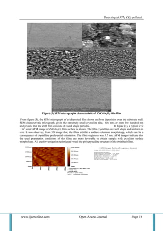
The surface morphology of the thin films was also investigated. SEM and AFM characteristic photographs
are shown in figure (3) and (4).
ZnO(100)
)
ZnO(002)
In2O3(400)](https://image.slidesharecdn.com/d0412015021-150113050942-conversion-gate02/85/Detecting-of-NH3-CO2-polluted-gases-by-using-ZnO-In2O3-thin-films-3-320.jpg)
![Detecting of NH3, CO2 polluted..
www.ijceronline.com Open Access Journal Page 20
3.3 Response to gases vapor
The experimental arrangement for sensitivity measurement for NH3, CO2 gases vapor is shown in figure (8).
Nitrogen gas was purged for 20 min to clean the sample environment, examined gases (NH3, CO2) was injected
by micro-syringe into test chamber and sensing characteristics of the sensor was then observed. The change in
electrical resistance of a sensor was measured by electrometer. The time taken by the sensor for all of resistance
was considered as response time of a sensor. The ratio of measured resistance before and after exposing the
sample surface to gas vapor gives the value of sensitivity [26], as it calculated from the equation (4). Figure (9)
shows the sensitivity of the sensor to gases.
S=│R (air) - R(gas)│/ R(air) …………………..….(4)
The sensing properties were studied at low concentrations (9 ppm) of gases vapor. The optioned results in
pyrolysis methods are promising for the preparation of sensitive and low cost gas sensor operating in room
temperatures. It can be fabricating sensor to detect variety of gases.
Figure (8) Experimental arrangement system for gas detecting
a=NH3b=CO2
Figure (7) Plot of (αhν)2
versus (hν) curve of ZnO -In2O3 thin film](https://image.slidesharecdn.com/d0412015021-150113050942-conversion-gate02/85/Detecting-of-NH3-CO2-polluted-gases-by-using-ZnO-In2O3-thin-films-6-320.jpg)
![Detecting of NH3, CO2 polluted..
www.ijceronline.com Open Access Journal Page 21
Figure (9:a,b) Sensitivity vs. time of ZnO-In2O3 thin film to NH3, CO2 gases
IV- CONCLUSION
Polycrystalline ZnO-In2O3 thin film sensor for NH3, CO2 gases has been prepared in pyrolysis method
successfully. The films have been characterized by x-ray diffraction, SEM microscopic and AFM microscopic.
From the optical properties of thin films we observe the optical gap which is about 3.11eV. The sensitivity of
the sensor to NH3, CO2 has been obtained at room temperature. The ratio of sensitivity of NH3 is better than CO2
vapor. This result obtained in pyrolysis methods are promising for the preparation of sensitive and low cost
NH3, CO2 sensor operating in room temperatures.
REFERENCES
[1] M. Wirtz J. Kluczik, M. Rivera, J. Am. Chem. Soc. 2000, 122, 1047–1056.
[2] C. A. Martinez, J. D. Stewart, Curr. Org. Chem. 2000, 4, 263–268.
[3] C. G. Granquist, Appl. A: Solids Surf. 1993, 57, 19–22.
[4] G. Haacke, J. Appl. Phys. 1976, 47, 4086–4089.
[5] C. Liu, T. Matsutani, N. Yamamato, M. Kiuchi, Europhys. Lett. 2002, 59, 606–610.
[6] Y. Zhizhen, M. Dewei, H. Junhui, J Crystal Growth 2003, 256, 78.
[7] Debabrata Pradhan, Shrey Sindhwani, K. T. Leung, Nanos-cale Res Lett 2010, 5, 1727.
[8] P. Puspharajah, S. Radhakrishna, J Mater Sci 1997, 32, 3001.
[9] G. Zhang, M. Adachi, S. Ganjil, A. Nakamura, J. Temmyo, Y. Matsui, Jpn. J. Appl. Phys. Part 2, 2007, 46, L730.
[10] C. Gorla, N. Emanetoglu, S. Liang, W. Mayo, Y. Lu, M. Wraback, H. Shen, J Appl Phys 2000,85, 2595.
[11] B. Sang, K. Kushiya, D. Okumura, O. Yamase, Sol Energy Mater Sol Cells 2001, 67, 237.
[12] M. Lorenz, E.M. Kaidashev, A. Rahm, Th. Nobis, J. Lenzner, G. Wagner, D. Spemann, H. Hochmuth, M. Grundmann, Appl.
Phys. Lett. 2005, 86, 143113.
[13] YR. Ryu, S. Zhu, JD. Budai, HR. Chandrasekhar, PF. Miceli, HW. White, Appl Phys Lett 2000, 88, 201.
[14] Y. Segawa, A. Ohtomo, M. Koinuma, ZK. Tang, P. Yu, GKL. Wong, Phys Stat Sol (b) 1997,202, 669.
[15] HB. Kang, K. Nakamara, SH. Lim, D. Shindo, Jpn J Appl Phys. 1998, 37, 781.
[16] C. Wang, B. Mao, E. Wang, Z. Kang, C. Tian, Solid State Commun. 2007, 141, 620.
[17] B. Liu, H.C. Zeng, Chem Mater 2007, 19, 5824.
[18] Y. Sun, N. George Ndifor-Angwafor, D.J. Riley, M.N.R. Ashfold, Chem. Phys. Lett. 2006, 431, 352.
[19] S. Kar, A. Dev, S. Chaudhuri, J. Phys. Chem. B 2006, 110, 17848.
[20] S.K.N. Ayudhya, P. Tonto, O. Mekasuwandumrong, V. Pa-varajarn, P. Praserthdam, Cryst. Growth Des. 2006, 6, 2446.
[21] C.V. Santilli, S.H. Pulcinelli, M.S. Tokumoto, V. Briois, J. Eur. Ceramic Soc. 2007, 27, 3691.
[22] P. Bhattacharyya, P.K. Basu, H. Saha, S. Basu, Sens. Actua-tors B Chem. B 2007,124, 62.
[23] S. Peulon, D. Lincot, Adv. Mater. 1996, 8, 166.
[24] W. Peng, S. Qu, G. Cong, Z. Wang, Cryst. Growth Des. 2006, 6, 1518.
[25] B. Cao and W. Cai, J. Phys. Chem. C 2008,112, 680.
[26] L. Znaidi, GJAA. Soler Illia, S. Benyahia, C. Sanchez, AV. Kanaev, Thin Solid Films, 2003, 428, 257.
[27] Li Wang, Yong Pu, Wenqing Fang, Jiangnan Dai, Changda Zheng, Chunlan Mo, Chuanbin Xiong and Fengyi Jiang, Thin Solid
Films, 2005,491, 323.
[28] K K Makhija, Arabinda Ray, R M Patel U B Trivedi And H N Kapse, Bell . Mater, Sci,. vol 28, no.1 2005, pp. 9-17.
[29] ICDD 1997 JCPDS International center for diffraction data A rights reserved PCPDFWIN v.1.30.
[30] R. Sarhaddi, N. Shahtahmasebi, M. Rezaee Rokn-Abadi, M.M. Bagheri-Mohagheghi, "Effect of post-annealing temperature on
nano-structure and energyband gap of indium tin oxide (ITO) nano-particles synthesized by polymerizing–complexing sol–gel
method" ,. physics E 43,(2010), 452-457
[31]. K.Girija, S.Thirumalairajan, S.M.Mohan, J.Chandrasekaran, "Structral, Morphological And Optical Studies Of Cdse Thin Films
From Ammonia Bath", Chalocogenide Letters Vol.6.No.8, August 2009, p.351-357.](https://image.slidesharecdn.com/d0412015021-150113050942-conversion-gate02/85/Detecting-of-NH3-CO2-polluted-gases-by-using-ZnO-In2O3-thin-films-7-320.jpg)


![Ultra smooth and lattice relaxed zn o thin films [eid]](https://cdn.slidesharecdn.com/ss_thumbnails/ultra-smoothandlatticerelaxedznothinfilmseid-141105101210-conversion-gate02-thumbnail.jpg?width=640&height=640&fit=bounds)


