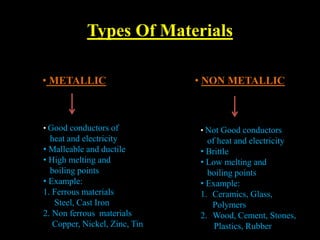
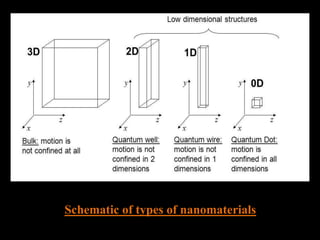
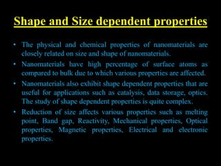
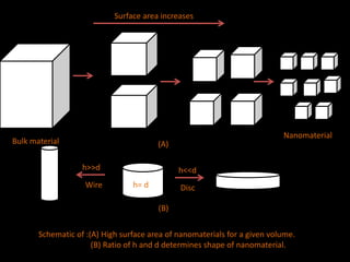
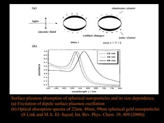
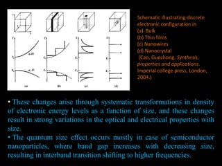
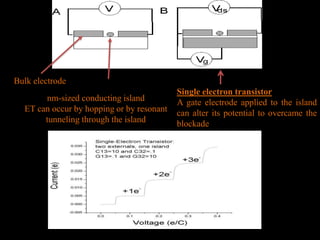
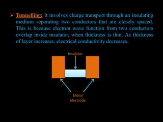
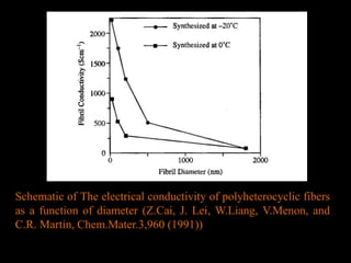
This document discusses the classification and properties of nanomaterials. It begins by describing the different types of nanomaterials based on dimensionality - zero-dimensional, one-dimensional, two-dimensional, and three-dimensional. It then explains how the physical and chemical properties of nanomaterials, such as melting point, band gap, mechanical strength, and optical absorption, are dependent on their size and shape due to increased surface area and quantum effects. The document concludes by discussing how electrical conductivity and other electronic properties are also influenced by the nanoscale dimensions.
In this presentation, you can find the general description of the Polymer Nano-Composites. About the Properties, they incorporate the Composite material.
The processing techniques of Polymer Nano-Composites as well.
In this presentation, you can find the general description of the Polymer Nano-Composites. About the Properties, they incorporate the Composite material.
The processing techniques of Polymer Nano-Composites as well.
Carbon Nanotubes(CNTs) | Characterisation and Purification methodsNitesh Sharma
Carbon nanotubes are one of the emerging materials developed in recent two decades. This report summarises the information of carbon nanotubes with their various synthesis techniques to produce CNTs. Different structures have been discussed like single-shell tubes, multi-shell tubes, bundles and cones. Notable state of the art characterization techniques like SEM, TEM, Raman Spectroscopy, Fourier Transform Infrared Spectroscopy, EDS, EDX, HRTEM has been also briefly discussed to study their structure- property correlation in this candidate material. Properties such as low dimensability, high surface-to-volume ratio is observed in carbon nanotubes. Unique mechanical, optical, electrical and electrochemical properties for carbon nanotubes are elaborately discussed here. Carbon nanotubes are advanced materials having tubular structure with nanometre diameter and large length/diameter ratio. Other properties such as density, stability is important for CNTs. Finally, prospects for carbon nanotubes are considered for carbon nanotubes.
LARGE PARTICLE REINFORCED COMPOSITE ,,,An Overview
Seminar done as a part of METALLURGY AND MATERIAL SCIENCE.
Good PPT to study,
included most of the points to study
HASEEB KM
S3 ME
MUTHOOT INSTITUTE OF TECHNOLOGY AND SCIENCE, COCHIN
It describes how different properties of materials changes when reduced to nano. Property includes electrical, optical, mechanical, magnetic, thermal etc.
The nanoscience is study of production of material of size as small as nanometer size, in practice a material should be of size between 1nm to 100nm at least one of three dimensions to be called a nanomaterial. The properties of material different from its bulk counterpart when it reduced its dimensions to nanoscale. Here some fundamentals about nanoscience, nanotechnology, properties and materials is discussed.
In this presentation, basics of solar cells, what is piezoelectricity and its application, followed by basics of thermoelectricity and its application would be discussed.
Zone melting is a key technique for single crystal growth fabrication. Zone melting is a group of techniques used to purify an element or compound and control its composition. This presentation will discuss the basics of the zone melting technique and with help of 2-3 research papers, the examples of zone melting would be explained. Single crystal growth is a quite useful technique used in various applications in the field of metallurgy as well as nanomaterials synthesis. The technique is used for the removal of unwanted impurities from the material, control the discontinuities in impurity distribution, and also maintaining uniform doping of the impurity in the material.
A key vacuum deposition technique for making highly homogenous and high-performance solid-state thin films and materials is Chemical vapor deposition. The types of CVD systems and their key applications would also be discussed in this presentation. It is a key bottom-up processing technique, widely used in graphene fabrication, also the fabrication of various oxides, nitrides is possible, with this technique.
the presentation gives brief description about magnetic nanoparticles, types of magnetic nanoparticles, magnetic nanocomposite and application of magnetic nanoparticles.
Carbon nanotubes are the next generation materials and in this presentation the application of Carbon nanotubes as fuel cell materials have been discussed.
Nanocomposite materials based on metal nanoparticles, metal oxide nanoparticles and magnetic nanoparticles have been discussed in this presentation. Hope the presentation is useful, you can request for download if you find the content useful.
An interesting phenomenon of Sub-Bragg diffreaction in 2D photonic crystals would be discussed here.
I would like to acknowledge Dr. R.V Nair, IIT Ropar for providing knowledge about such an interesting topic.
Welcome to WIPAC Monthly the magazine brought to you by the LinkedIn Group Water Industry Process Automation & Control.
In this month's edition, along with this month's industry news to celebrate the 13 years since the group was created we have articles including
A case study of the used of Advanced Process Control at the Wastewater Treatment works at Lleida in Spain
A look back on an article on smart wastewater networks in order to see how the industry has measured up in the interim around the adoption of Digital Transformation in the Water Industry.
Cosmetic shop management system project report.pdfKamal Acharya
Buying new cosmetic products is difficult. It can even be scary for those who have sensitive skin and are prone to skin trouble. The information needed to alleviate this problem is on the back of each product, but it's thought to interpret those ingredient lists unless you have a background in chemistry.
Instead of buying and hoping for the best, we can use data science to help us predict which products may be good fits for us. It includes various function programs to do the above mentioned tasks.
Data file handling has been effectively used in the program.
The automated cosmetic shop management system should deal with the automation of general workflow and administration process of the shop. The main processes of the system focus on customer's request where the system is able to search the most appropriate products and deliver it to the customers. It should help the employees to quickly identify the list of cosmetic product that have reached the minimum quantity and also keep a track of expired date for each cosmetic product. It should help the employees to find the rack number in which the product is placed.It is also Faster and more efficient way.
NO1 Uk best vashikaran specialist in delhi vashikaran baba near me online vas...Amil Baba Dawood bangali
Contact with Dawood Bhai Just call on +92322-6382012 and we'll help you. We'll solve all your problems within 12 to 24 hours and with 101% guarantee and with astrology systematic. If you want to take any personal or professional advice then also you can call us on +92322-6382012 , ONLINE LOVE PROBLEM & Other all types of Daily Life Problem's.Then CALL or WHATSAPP us on +92322-6382012 and Get all these problems solutions here by Amil Baba DAWOOD BANGALI
#vashikaranspecialist #astrologer #palmistry #amliyaat #taweez #manpasandshadi #horoscope #spiritual #lovelife #lovespell #marriagespell#aamilbabainpakistan #amilbabainkarachi #powerfullblackmagicspell #kalajadumantarspecialist #realamilbaba #AmilbabainPakistan #astrologerincanada #astrologerindubai #lovespellsmaster #kalajaduspecialist #lovespellsthatwork #aamilbabainlahore#blackmagicformarriage #aamilbaba #kalajadu #kalailam #taweez #wazifaexpert #jadumantar #vashikaranspecialist #astrologer #palmistry #amliyaat #taweez #manpasandshadi #horoscope #spiritual #lovelife #lovespell #marriagespell#aamilbabainpakistan #amilbabainkarachi #powerfullblackmagicspell #kalajadumantarspecialist #realamilbaba #AmilbabainPakistan #astrologerincanada #astrologerindubai #lovespellsmaster #kalajaduspecialist #lovespellsthatwork #aamilbabainlahore #blackmagicforlove #blackmagicformarriage #aamilbaba #kalajadu #kalailam #taweez #wazifaexpert #jadumantar #vashikaranspecialist #astrologer #palmistry #amliyaat #taweez #manpasandshadi #horoscope #spiritual #lovelife #lovespell #marriagespell#aamilbabainpakistan #amilbabainkarachi #powerfullblackmagicspell #kalajadumantarspecialist #realamilbaba #AmilbabainPakistan #astrologerincanada #astrologerindubai #lovespellsmaster #kalajaduspecialist #lovespellsthatwork #aamilbabainlahore #Amilbabainuk #amilbabainspain #amilbabaindubai #Amilbabainnorway #amilbabainkrachi #amilbabainlahore #amilbabaingujranwalan #amilbabainislamabad
Hierarchical Digital Twin of a Naval Power SystemKerry Sado
A hierarchical digital twin of a Naval DC power system has been developed and experimentally verified. Similar to other state-of-the-art digital twins, this technology creates a digital replica of the physical system executed in real-time or faster, which can modify hardware controls. However, its advantage stems from distributing computational efforts by utilizing a hierarchical structure composed of lower-level digital twin blocks and a higher-level system digital twin. Each digital twin block is associated with a physical subsystem of the hardware and communicates with a singular system digital twin, which creates a system-level response. By extracting information from each level of the hierarchy, power system controls of the hardware were reconfigured autonomously. This hierarchical digital twin development offers several advantages over other digital twins, particularly in the field of naval power systems. The hierarchical structure allows for greater computational efficiency and scalability while the ability to autonomously reconfigure hardware controls offers increased flexibility and responsiveness. The hierarchical decomposition and models utilized were well aligned with the physical twin, as indicated by the maximum deviations between the developed digital twin hierarchy and the hardware.
Hybrid optimization of pumped hydro system and solar- Engr. Abdul-Azeez.pdffxintegritypublishin
Advancements in technology unveil a myriad of electrical and electronic breakthroughs geared towards efficiently harnessing limited resources to meet human energy demands. The optimization of hybrid solar PV panels and pumped hydro energy supply systems plays a pivotal role in utilizing natural resources effectively. This initiative not only benefits humanity but also fosters environmental sustainability. The study investigated the design optimization of these hybrid systems, focusing on understanding solar radiation patterns, identifying geographical influences on solar radiation, formulating a mathematical model for system optimization, and determining the optimal configuration of PV panels and pumped hydro storage. Through a comparative analysis approach and eight weeks of data collection, the study addressed key research questions related to solar radiation patterns and optimal system design. The findings highlighted regions with heightened solar radiation levels, showcasing substantial potential for power generation and emphasizing the system's efficiency. Optimizing system design significantly boosted power generation, promoted renewable energy utilization, and enhanced energy storage capacity. The study underscored the benefits of optimizing hybrid solar PV panels and pumped hydro energy supply systems for sustainable energy usage. Optimizing the design of solar PV panels and pumped hydro energy supply systems as examined across diverse climatic conditions in a developing country, not only enhances power generation but also improves the integration of renewable energy sources and boosts energy storage capacities, particularly beneficial for less economically prosperous regions. Additionally, the study provides valuable insights for advancing energy research in economically viable areas. Recommendations included conducting site-specific assessments, utilizing advanced modeling tools, implementing regular maintenance protocols, and enhancing communication among system components.
2. Types Of Materials
• METALLIC • NON METALLIC
• Good conductors of
heat and electricity
• Malleable and ductile
• High melting and
boiling points
• Example:
1. Ferrous materials
Steel, Cast Iron
2. Non ferrous materials
Copper, Nickel, Zinc, Tin
• Not Good conductors
of heat and electricity
• Brittle
• Low melting and
boiling points
• Example:
1. Ceramics, Glass,
Polymers
2. Wood, Cement, Stones,
Plastics, Rubber
3. Types of Nanomaterials
• Zero dimensional (0D) – In this all dimensions are reduced to nm
range, movement of electron is restricted all three x, y, z directions.
Eg: Quantum dots, nanoparticles.
• One dimensional (1D)- In this two dimensions are reduced to nm
range and one dimension remains large and electron is allowed to
move along this dimension. Eg: Nanowires, Nanorods.
• Two dimensional (2D)- In this one dimension is confined to nm range
and two dimensions remain large and electron is allowed to move
along these two directions. Eg: Nanowells, Nanofilms, Nanocoatings.
• Three dimensional (3D)- In this there is no confinement in
nanorange and electron movement is allowed in all three x, y, z
directions. Eg: Bulk nanomaterials, Nanopowders.
5. Shape and Size dependent properties
• The physical and chemical properties of nanomaterials are
closely related on size and shape of nanomaterials.
• Nanomaterials have high percentage of surface atoms as
compared to bulk due to which various properties are affected.
• Nanomaterials also exhibit shape dependent properties that are
useful for applications such as catalysis, data storage, optics.
The study of shape dependent properties is quite complex.
• Reduction of size affects various properties such as melting
point, Band gap, Reactivity, Mechanical properties, Optical
properties, Magnetic properties, Electrical and electronic
properties.
6. Bulk material
Nanomaterial
Surface area increases
(A)
h>>d
h= d
h<<d
Wire Disc
(B)
Schematic of :(A) High surface area of nanomaterials for a given volume.
(B) Ratio of h and d determines shape of nanomaterial.
9. Melting point dependence on size
• • Start from an energy balance; assume the change in internal en
• (∆U) and change in entropy per unit mass during melting are
• independent of temperature
• Start from an energy balance; assume the change in internal energy
(∆U) and change in entropy per unit mass during melting are
independent of temperature
Lr
To
/
2
∆ = Deviation of melting point from the bulk value
To = Bulk melting point
= Surface tension coefficient for a liquid-solid interface
= Particle density
r = Particle radius
L = Latent heat of fusion
10. • Lowering of the melting point is proportional to 1/r
• can be as large as couple of hundred degrees when the
particle size gets below 10 nm!
• Most of the time, the surface tension coefficient is unknown;
by measuring the melting point as a function of radius, can
be estimated.
• Note: For nanoparticles embedded in a matrix, melting point
may be lower or higher, depending on the strength of the
interaction between the particle and matrix.
11. Band Gap
• Band gap is the energy separation between Conduction band and valence
band.
• In bulk materials, there are 1023 atoms on surface, large no. of atoms means
large energy states, so band gap is less.
• As we go in nanorange, no. of atoms decrease to 10-1000 atoms, so energy
states decrease, band gap is more.
Eg
Bulk material
Eg
Nanomaterial
12. Mechanical Properties
• The mechanical properties of nanomaterials increase with
decrease in size, because smaller the size, lesser is the
probability of finding imperfections such as dislocations,
vacancies, grain boundaries.
• Strength of material improves significantly as the particle size
decrease due to perfect defect free surface.
• Hardness and yield strength of material also increases as
particle size is decreased.
• Elastic modulus and toughness of material also increases as
particle size is decreased.
13. Optical Properties
• The reduction of material dimension has pronounced effect on
optical properties.
• Size dependence is due to:
Surface Plasmon Resonance (SPR)
Quantum size effects
14. Surface Plasmon Resonance (SPR)
• SPR is process which takes place when there is coherent
oscillation of conduction band electrons upon interaction with
an electromagnetic field.
• It takes place when size of nanoparticle is smaller than
wavelength of incident radiations.
• It occurs mostly in case of metal nanoparticles such as gold
nanoparticles.
Figure: Schematic of
Plasmon oscillation for a
sphere, showing the
displacement of the
conduction electron charge
cloud relative to the nuclei.
15. Surface plasmon absorption of spherical nanoparticles and its size dependence.
(a) Excitation of dipole surface plasmon oscillation
(b) Optical absorption spectra of 22nm, 48nm, 99nm spherical gold nanoparticles
(S Link and M.A. El- Sayed, Int. Rev. Phys. Chem. 19, 409 (2000))
16. • Electric field of incoming light wave causes polarization of free
electrons w.r.t to heavier ionic core of spherical nanoparticle. A net
charge difference is seen at nanoparticle surface, which acts as a
restoring force . In this manner a dipolar oscillation of electrons is
created with period T.
• SPR is dipolar excitation of entire particle between negatively
charged free electrons and positively charged lattice.
• The value of SPR depends on free electron density and dielectric
medium surrounding the nanoparticle.
• SPR effect occurs in noble metal nanoparticles, which gives rise to
sharp and intense absorption band in visible range (shown in fig (b)).
Plasmon band red shifts with increasing particle size. The increase of
both absorption wavelength and peak width with increasing particle
size can be clearly seen from figure.
• The color of nanoparticle depends on both size and shape of
nanoparticle. Eg: Spherical shape gold nanoparticle gives red color,
flat gold nanoparticles give blue color.
17. Quantum size effects
• The unique optical properties of nanomaterials also arise due
to quantum size effects.
• When size of nanocrystal is smaller than De-Broglie
wavelength, electrons and holes are spatially confined and
electric dipoles are formed, discrete energy levels are also
formed.
• Similar to particle in box, energy separation between adjacent
levels increases with decreasing dimensions.
18. AA
• These changes arise through systematic transformations in density
of electronic energy levels as a function of size, and these changes
result in strong variations in the optical and electrical properties with
size.
• The quantum size effect occurs mostly in case of semiconductor
nanoparticles, where band gap increases with decreasing size,
resulting in interband transition shifting to higher frequencies.
Schematic illustrating discrete
electronic configuration in
(a) Bulk
(b) Thin films
(c) Nanowires
(d) Nanocrystal
(Cao, Guozhong. Synthesis,
properties and applications.
Imperial college press, London,
2004.)
19. Magnetic properties
• Magnetic properties of nanomaterials differ to that of bulk.
• For a ferromagnetic material, total energy is
Etot = Eexc + Eani + Edem + Eapp
Eexc = Exchange energy, Eani = Anisotropic energy
Edem = Demagnetization energy
Eapp = Energy due to applied magnetic field
Etot = M.H
• For nanomaterials, important consideration is interaction among
exchange energy, anisotropic energy and demagnetization energy.
• For small grain sizes, exchange forces are dominant due to strong
coupling causing all spins in neighbouring atoms to align.
20. • There exists a small diameter, below which material will be
single domain
2
0
9
S
B
Cri
M
D
where
γB = 4(AK1)1/2
A = Exchange stiffness
K1 = Anisotropic constant
µ0 = Permittivity of free space
Ms = Saturation magnetization
K1
K1
•Example : critical diameter for Co is 70 nm, Fe is 15 nm
• As size of particle becomes smaller than critical diameter,
magnetization becomes unstable and loss of magnetization takes
place and ferromagnetic material becomes superparamagnetic.
21. • The coercive field of ferromagnetic material increases with
decreasing particle size, with maxima within the critical diameter
range. If further particle size decreases, coercive field
significantly reduces until the magnetization becomes unstable
due to superparamagnetic behaviour. At this stage hysteresis loop
is completely removed. Eg: Nanoscale amorphous Fe-Ni-Co
compounds with 10-15nm grain size shows no hysteresis.
• Magnetization reversal also becomes insignificant when size of
particle decreases.
• As size of particle decreases, saturation magnetization increases.
Eg: for Zn Ferrite, saturation magnetization increases for particle
of size 20 nm. This enhancement of magnetization restricts the
rotation of magnetization vector by thermal motion, which is
helpful in magnetic recording applications.
22. Electrical and Electronic Properties
• Size plays an important role in electrical properties and is
based on 4 mechanisms:
Surface scattering
Change of electronic structure
Quantum transport
Effect of microstructure
23. Surface scattering
• Electrical conductivity of metals is described by various electron
scattering phenomenon and total resistivity is combination of
individual and independent scattering known as Matthiessen’s rule.
ρT = ρTh + ρD
where ρTh is thermal resistivity, ρD is defect resistivity
• Impurity atoms, defect such as vacancies, grain boundaries disrupt
electric potential of lattice and cause electron scattering.
• Considering individual electrical resistivity inversely proportional to
the respective mean free path (λ) between collisions, the
Matthiessen’s rule can be written as:
1/λT=1/ λTh+1/ λD
24. • Reduction in material’s dimensions will increase crystal perfection
or reduction of defects, which would result in a reduction in defect
scattering and, thus a reduction in resistivity and conductivity
increases.
• In nanowires and thin films, the surface scattering of electrons
results in reduction of electrical conductivity. When the critical
dimension is smaller than the mean free path, motion of electron
will undergo elastic and inelastic scattering.
Elastic scattering: electron reflects same way as photon reflects
from mirror. Both momentum and energy is conserved. Direction of
motion of electron is parallel to surface. Electrical conductivity is
same as bulk materials.
Inelastic scattering: In this electron mean free path is terminated
by impinging on surface. The electron loses its kinetic energy and
electrical conductivity decreases.
25. Change of Electronic structure
• Reduction in characteristic dimension below a critical size, i.e.
below De Broglie wavelength results in change of electronic
structure, leading to widening of band gap. Such a change results
in reduced electrical conductivity.
• Some metal nanowires undergo transition to become
semiconductors and semiconductors might become insulators
when their diameters are reduced below a critical diameter.
26. Quantum transport
• It includes Ballistic conduction, Coulomb blockade and tunnelling.
Ballistic conduction: It occurs when length of conductor is
smaller than electron mean free path. In this case, each transverse
waveguide mode or conducting channel contributes G0 = 2e2h =
12.9kΩ-1
• In ballistic transport there is no energy dissipation and no elastic
scattering takes place. When elastic scattering occurs, transmission
coefficients and electrical conductance is reduced. The ballistic
transport was first reported in Carbon nanotubes (CNTs).
27. Coulomb blockade: It occurs when length of contact
resistance is larger than resistance of nanostructures and total
capacitance of object is so small that adding a single electron
requires significant energy.
• Metal or semiconductor nanocrystals exhibit quantum effects
that give rise to discrete charging of metal particles. Such a
electron configuration permits one to pick up electric charge
one electron at a time at specific voltage values. This Coulomb
blockade behaviour is also known as Coulombic staircase and
finds use in Single electron transistors (SETs).
• Electron can move from one energy level to another when it
has charging energy e2/2C.
28. Bulk electrode
nm-sized conducting island
ET can occur by hopping or by resonant
tunneling through the island
Single electron transistor
A gate electrode applied to the island
can alter its potential to overcame the
blockade
29. Tunnelling: It involves charge transport through an insulating
medium seperating two conductors that are closely spaced.
This is because electron wave function from two conductors
overlap inside insulator, when thickness is thin. As thickness
of layer increases, electrical conductivity decreases.
Metal
electrode
Insulator
30. Effect of microstructure
• Electrical conductivity may change due to formation of
ordered microstructure, when size is reduced to nm range.
• For example, polymer fibers demonstrated an increase in
electron conductivity.
• When polymer size is reduced to nm size, polymers are
aligned parallel to the axis of the fibers, which results in
increased contribution of intramolecular conduction and
reduced intramolecular conduction.
• A drastic increase in electrical conductivity was found at 500
nm.
• Smaller the diameter, better alignment of polymers and thus
higher the electrical conductivity.
31. Schematic of The electrical conductivity of polyheterocyclic fibers
as a function of diameter (Z.Cai, J. Lei, W.Liang, V.Menon, and
C.R. Martin, Chem.Mater.3,960 (1991))
32. Introduction to Nanoplasmonics
• Nanoplasmonics is the study of optical phenomenon (control and
monitoring of localization of optical energy) in nanoscale vicinity of
metal surfaces (2-20 nm).
• This field is thought to be new, but numerous examples of its basic
principles can be found from as long as 4th Century AD.
• Lycurgus cup from British museum is a fascinating object, its glass
looks green in reflected light (eg, if we click picture with flash) and
ruby red in transmitted light (picture taken with light behind the
object). It was found that this dichroic glass contains nanocrystals of
gold-silver alloy in less than 1% of cup. These metallic
nanoparticles can both absorb and scatter light, intensity of light
transmitted depends on viewing and incident angles.
33. Lycurgus cup, taken from nature photonics,
2007(Stockman, Mark I. "Nanoplasmonics:
The physics behind the applications." Phys.
Today 64.2 (2011): 39-44.)
34. • A remarkable property of such systems is ability to keep optical
energy on nanoscale due to modes called surface plasmons (SPs).
• Plasmons is 3D crystal of positively charged ions with delocalized
electron gas moving in periodic potential of ion grid.
• Surface plasmons are the plasmons confined to surface and interact
strongly with light.
• The existence of SPs depend on the fact that dielectric function (εm)
has a negative real part i.e. Reεm < 0 and these occur when losses
are small enough Imεm << -Reεm .
Figure: Schematic of
Plasmon oscillation for a
sphere, showing the
displacement of the
conduction electron charge
cloud relative to the nuclei.
35. Important terms in Nanoplasmonics
• Quality factor: It determines how many oscillation a SP undergo before it
decays and also measure increase in local field amplitude when SPs are in
resonance.
• Modal volume: It is the volume in which SP is localized and is usually of
the order of volume of nanoparticle, about 10nm3.
• Oscillatory strength (f): It is equal number of conduction electrons in a
particle, ~ 105 , for a quantum dot f =1. Absorption is directly propotional
to f, while scattering is propotional to square of f., so plasmonic
nanoparticles are efficient scatterers and absorbers.
• Lifetime of SP is (2γ)-1
)
(
2
)
(
2
m
m
m
e
I
R
Q
where γ is decay rate of plasmonic field
36. Hot spots
• It is a very important phenomenon in Nanoplasmonics.
• On nm scale, every plane wave looks like a uniform plane
wave, however when light is incident on nanoplasmonic
particles, it gives rise to an inhomogenous distribution of
intense and highly localized electric fields. These intensity
spikes are known as hot spots.
• Hot spots arise due to:
Surface plasmon resonance (SPR)
Constructive interference of fields from different SPs.
Specific geometries such as sharp tip or narrow gaps.
37. Application of Nanoplasmonics
• Biomedical applications
Linking specific antibody to metal surface, tumor cells can be
targetted and imaged before pathologic changes occur. HIV
virus can be detected with Ag nanoparticles.
• Sensing
To monitor glucose level of diabetics, another sensing
application is based on red shift of localized SP resonances in
response to covering metal surface with analyte molecules.
• Plasmonic integrated circuits
• Waveguides