Download as PDF, PPTX
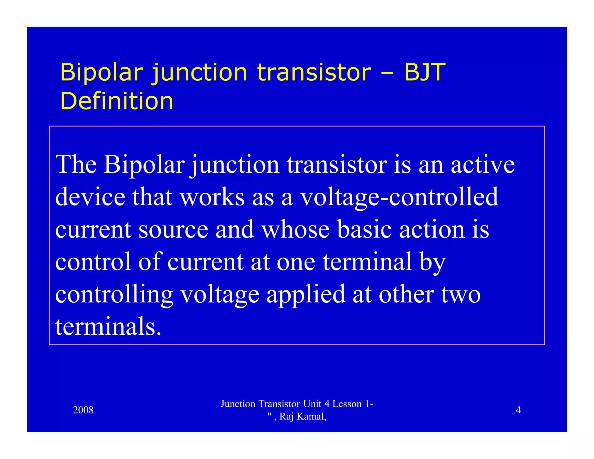
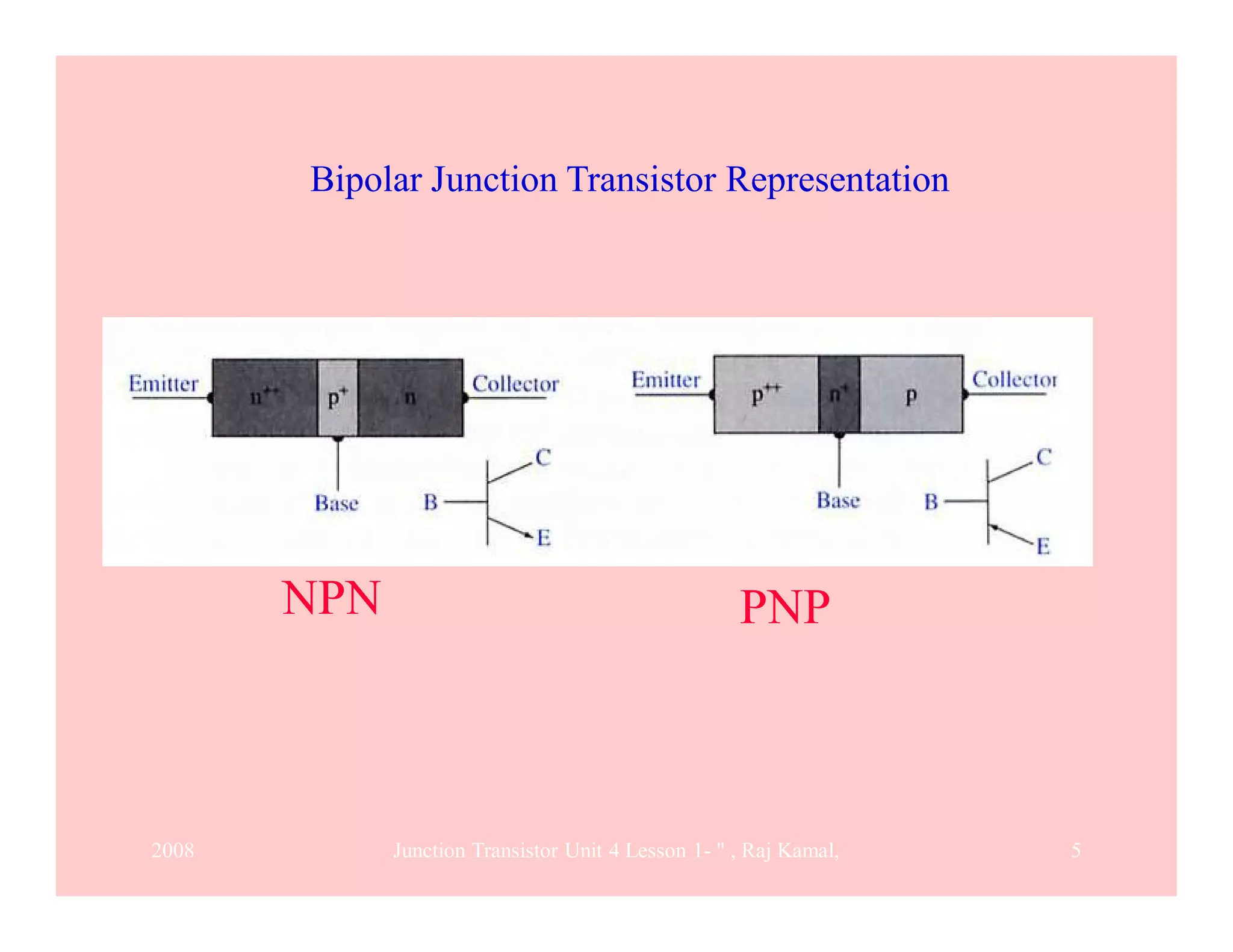
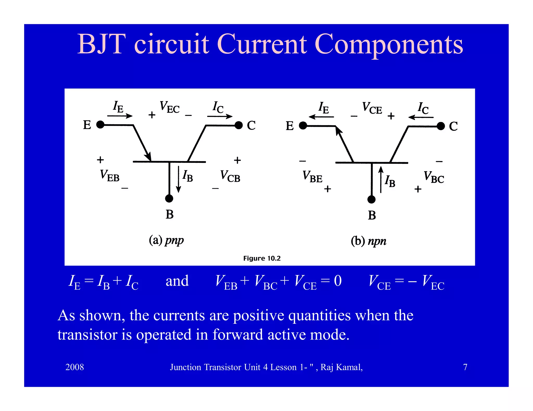
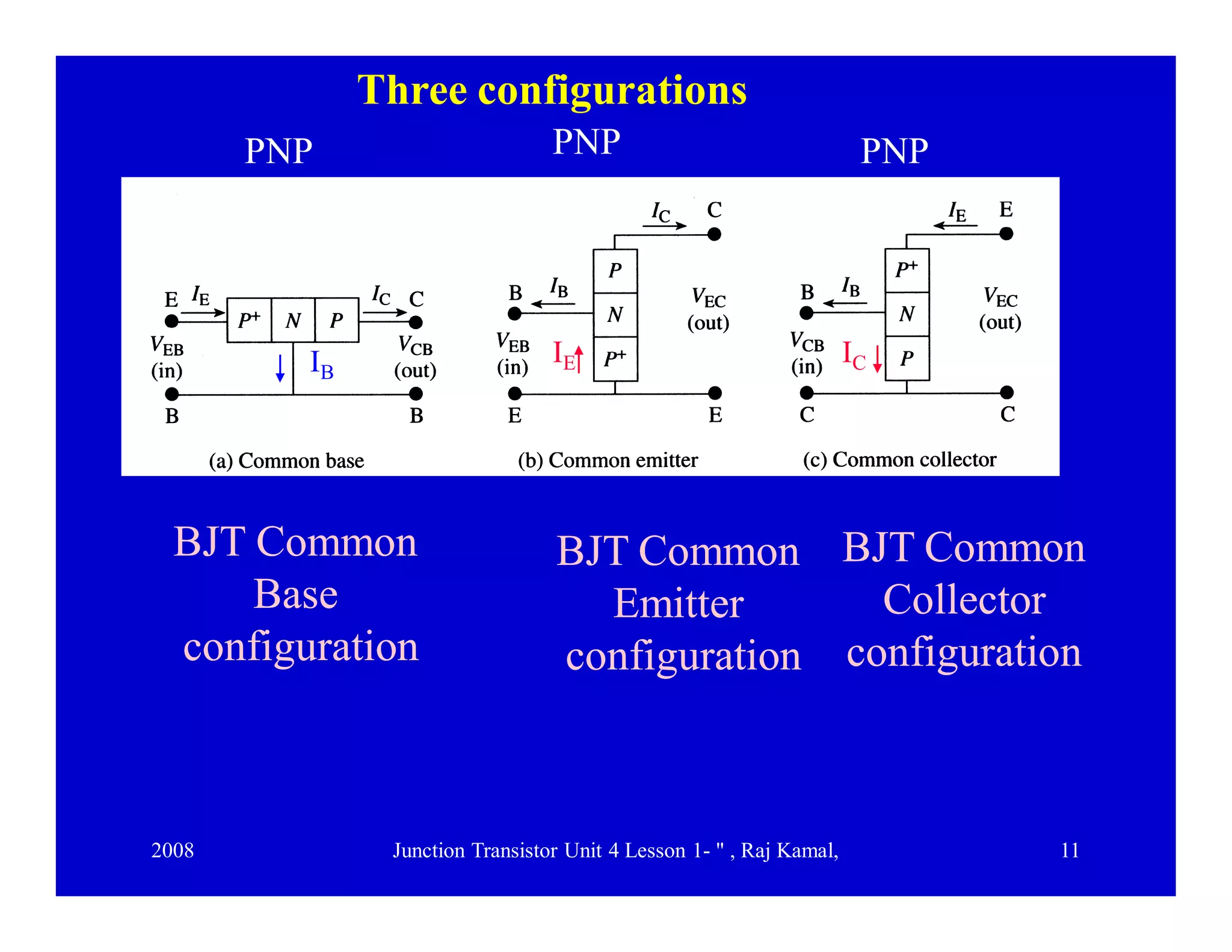
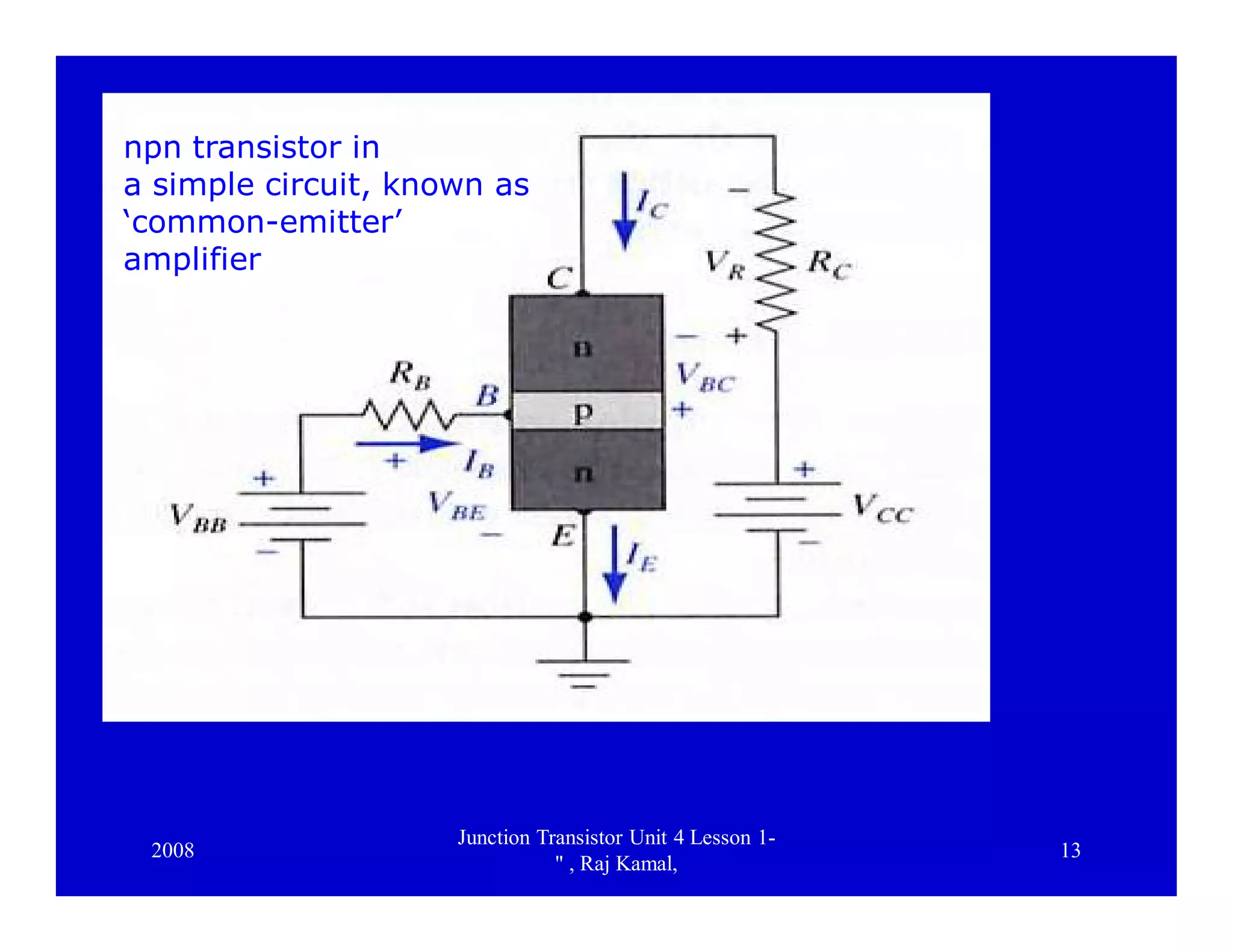
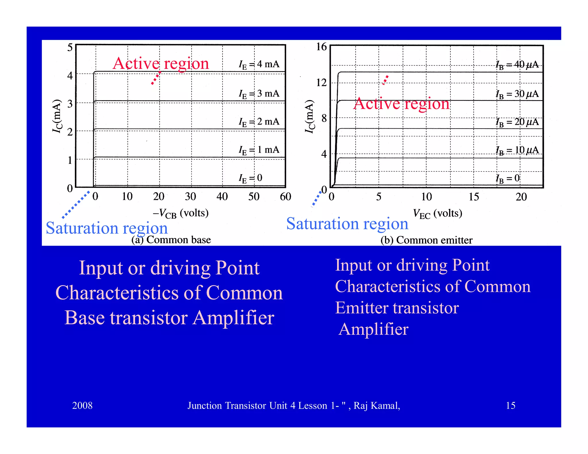
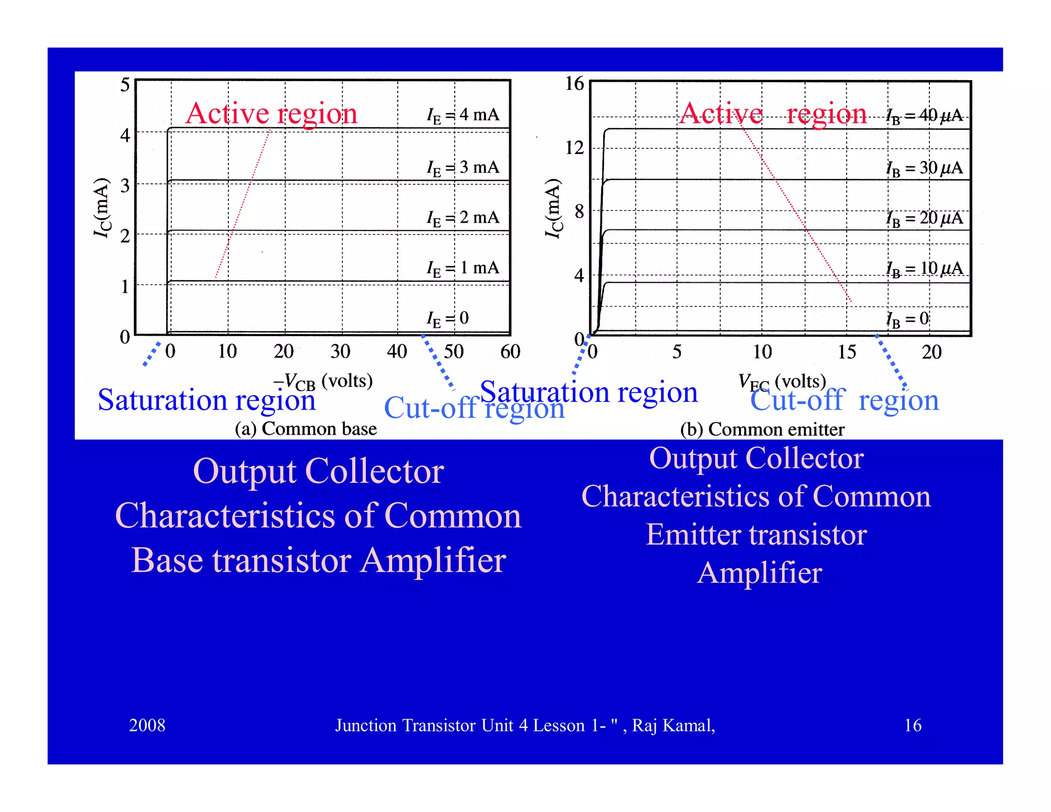

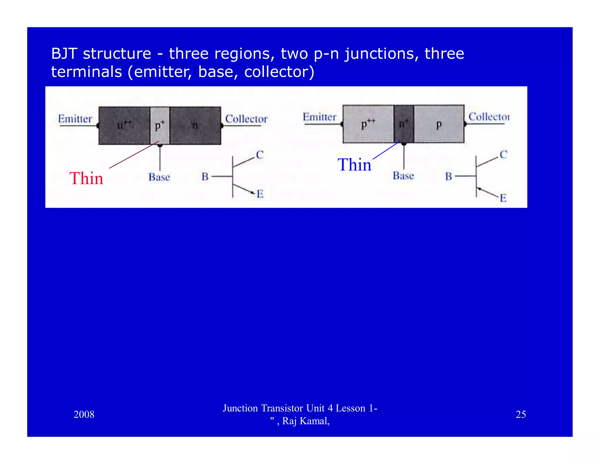


The document provides an overview of junction transistors, specifically focusing on bipolar junction transistors (BJTs), their definitions, characteristics, and different configurations such as common base, common emitter, and common collector. It discusses the modes of operation including forward biasing, reverse biasing, and the different regions of operation: cut-off, saturation, and active. Key aspects of BJT construction and current components in circuits are also highlighted.


