AVR_Course_Day2 what is pcb
•
9 likes•1,419 views

This is a microcontroller course for atmega328 (the chip used in Arduino Uno) explained very simply .
Report
Share
Report
Share

Recommended
Pcb design powerpoint
This document provides guidelines for PCB design, including key principles of current flow, coupling, and stackup goals. It discusses protection devices, power generation, routing traces, vias, copper pours, grounding, decoupling capacitors, component selection, circuit mounting, and layout programs. Manufacturers for PCB ordering are also listed.
PCB DESIGN - Introduction to PCB Design Manufacturing
This PPT Gives information about:
1. PCB computer aided manufacturing,
2. Panelization,
3. Copper patterning,
4. Subtractive, additive and semi-additive processes Patterning 5. method by volume,
6. Large volume,
7. Small volume,
8. Hobbyist,
9. Chemical etching
PCB Designing
Sorry to say but the college spelling is wrong actually "technology" word is missing. Its by mistake.
A presentation on printed circuit board designing. A brief discussion on pcb fabrication. Basic steps involved in it.
PPT ON PCB DESIGN INTERNSHIP
This document provides details about Sujoy Halder's internship training in PCB design from July 1, 2021 to August 3, 2021 at Internshala Training. It includes an introduction to printed circuit boards covering materials, components, and manufacturing processes. It also describes the use of EAGLE software for schematic capture and PCB layout. Specific topics covered include surface mount technology, routing, heat dissipation, and creating a power supply board. Sujoy received a certificate of completion after scoring 51% on the final assessment.
PCB Designing
PCBs are non-conductive boards that hold electronic components and allow electricity to flow through circuitry etched onto their surfaces, and they have been used since the 1940s in devices like radios, computers, and appliances; PCBs can be single sided, double sided, or multilayered and come in rigid, flexible, or rigid-flex styles to suit different applications; They connect components like resistors, capacitors, and ICs through pads and traces on one or more metal layers.
Printed circuit board
PCBs are non-conductive boards that hold electronic components connected by copper traces. They minimize wiring and space in electronic circuits. PCBs can be single sided, double sided, or multi-layered. Components include active parts like transistors and ICs or passive parts like resistors and capacitors. PCBs are designed then mass produced through processes like etching, drilling, and assembly. They are widely used in applications such as medical devices, military systems, aerospace equipment, and telecommunications infrastructure.
PCB Fabrication Process by Sierra Assembly
Step by step guide which will help to understand the PCB fabrication process. PCB manufacturing and assembly must be conducted in a clean environment that is free of contaminants. This is important to produce good quality boards that offer unfailing service for years.
Pcb designing
A printed circuit board (PCB) is a non-conductive laminated substrate that mechanically supports and electrically connects electronic components using copper tracks, pads and other features etched onto copper sheets. PCBs have evolved from early point-to-point wiring to modern surface mount and multilayer board designs. Key aspects of PCBs include the substrate material (often FR-4 fiberglass), copper patterning process (subtractive or additive), drilling of holes, plating, solder mask and the assembly of electronic components. Modern PCB design utilizes computer-aided manufacturing systems to efficiently layout, simulate and produce circuit boards.
pcb
This document discusses printed circuit boards (PCBs). It provides an introduction and overview of what a PCB is, the need for PCBs, types of PCBs including general, trace, single layer and double layer, and the design process for trace PCBs. It also outlines some advantages like lower costs for mass production and reduced wiring, and disadvantages such as difficulty repairing or redesigning a PCB. Finally, it provides some examples of PCB applications.
How does your Stack-up, stack up?
In this webinar, you'll learn:
Why your stackup is critical to overall design success
Key elements that comprise PCB board stack-ups (power planes, balance, flex / rigid-flex, etc)
Material selection tips and guidelines
Considerations for determining the optimal layer count
Determining impedance targets and how your stack-up affects your ability to meet your impedance goals
How to leverage your stackup to ensure design accuracy and good signal quality with your CAD system
An overview of embedding components and the costs/benefits
Printed circuit Board Description
The document discusses printed circuit boards (PCBs) and their evolution and classifications. It explains that PCBs provide electrical connections between circuit components using conductive tracks on a non-conductive substrate. Early electronic designs used point-to-point wiring but PCBs allowed for more reliable connections. Basic PCB types include single-sided, double-sided, and multilayer boards. More advanced types include rigid-flex boards, which combine rigid and flexible areas to fit devices. Proper PCB design is important to address issues like signal interference at high frequencies.
Pcb manufacturing
This document provides an overview of printed circuit board (PCB) manufacturing. It discusses various stages of the PCB manufacturing process including laminate fabrication, copper deposition, photolithography, etching, drilling, surface finishing techniques like solder masking and hot air leveling. It also covers different types of PCBs like single sided, double sided, multilayer and flexible PCBs. Various material options for PCB substrates and their properties are described. Manufacturing processes for different PCB components are outlined.
Introduction to PCB Design
A printed circuit board (PCB) is a non-conductive board that mechanically supports and electrically connects electronic components using copper tracks etched onto laminated sheets. PCBs can be single-sided, double-sided, or multilayer. They were first developed in the 1930s and are used to build circuit board assemblies, with common types including single-sided, double-sided, and multilayer boards.
PCB Layout Fundamentals
These are the slides from the very popular webcast 'PCB Layout Fundaments'. View it, download it or share it with a friend! By Analog Devices, Inc.
Rs 422
RS-422 is a telecommunications standard for binary serial communications between devices such as computers and printers. It uses a balanced four-wire system with two wires for transmitting from the data terminal equipment to the data communications equipment and two wires for transmitting in the opposite direction. RS-422 has advantages over RS-232 such as higher data rates, longer cable lengths, and better noise rejection, though it is only unidirectional and less common.
Pcb designing
This document discusses printed circuit board (PCB) design. It begins with an introduction to PCBs, describing how they mechanically support and electrically connect electronic components using conductive tracks on insulating substrates. It then discusses the basic materials that make up PCBs like copper foil and plating. The document outlines the main fabrication steps for PCBs which include setting up, imaging, etching, drilling, masking, and electrical testing. It also describes the characteristics of through-hole and surface mount technology. The etching and assembly processes are explained in more detail. Finally, the document provides an overview of PCB design and routing software like EAGLE and includes an example of a power supply board.
Package fabrication technolog ynew
This document discusses package fabrication technology. It begins by defining packaging as the technology required between an integrated circuit and the system level. There are three main levels of packaging - chip, board, and system level. The major functions of packaging are signal distribution, power distribution, heat dissipation, and protection from mechanical, chemical and electromagnetic stresses. Package fabrication technologies include refractory ceramic and molded plastic, and are either through-hole or surface mount. Key aspects covered include chip-to-package interconnections using wire bonding, TAB, flip chip, and chip-on-board approaches. 3D packaging technology is also summarized.
Printed board circuit design (Pcb) PPT
The document discusses printed circuit board (PCB) design. It begins by introducing PCBs and their history. It then describes the main types of PCBs and basic PCB terminology. The document outlines the general PCB design process from schematic design to routing to generating output files for fabrication. It provides guidelines for component placement and introduces PCB design rules to ensure sufficient spacing and avoid electrical issues. Finally, it briefly summarizes the key topics covered in the document.
Pcb layout
This document provides an overview of printed circuit boards (PCBs), including what they are, common materials, types, parts, pros and cons, layout issues, electromagnetic interference (EMI), and design process. PCBs electrically connect electronic components using conductive tracks laminated onto a non-conductive substrate. Key topics covered include signal routing, component placement, layer stacking, and techniques to reduce EMI such as ground plane segmentation and trace spacing. The conclusion emphasizes minimizing inductance to reduce emissions through optimal component placement and shortest possible high-speed signal routes.
Current mode circuits & voltage mode circuits
This document discusses current mode and voltage mode circuits. It begins by defining voltage mode and current mode circuits, noting that the definitions are not entirely precise as every circuit has both voltages and currents. It then provides examples of current mode circuits including the bipolar junction transistor and current mirror. It discusses how current mode and voltage mode signaling works for interconnects in integrated circuits. It notes several advantages of current mode circuits including lower power consumption and higher speed. It also discusses differences between the two modes and reasons for switching to current mode circuits such as easier compensation and better operation in continuous and discontinuous conduction modes. Potential disadvantages of current mode are also outlined like current sensing challenges and subharmonic oscillations.
pcb layers in layout
This document discusses the different types of layers used in a printed circuit board (PCB) layout. It describes 11 layers: the global layer defines component boundaries; the top and bottom layers are where components are mounted; inner layers separate top and bottom layers in multilayer PCBs; solder mask layers protect copper traces; solder paste layers define solder areas; silk screen layers contain text and markings; assembly layers define component shapes; and drill layers specify hole diameters. Each layer serves a distinct purpose in the PCB design and manufacturing process.
PCB designing and Manufacturing
You fill find all the basics you need to know about PCB and its types and also all information regarding the manufacturing process
Introduction to Hardware Design Using KiCAD
This presentation provides brief introduction about Hardware design basics. This also briefs about Hardware Design Process like Hardware Architecture Design, Schematics Design, PCB Layout Design. Introduction about KiCAD, open source EDA automation suite.
Design for Manufacturing (DFM) and Why it Matters
Prevent time-to-market delays by identifying manufacturing issues before they become a costly mistake. It’s not uncommon for designs to be submitted to manufacturing only to have problems identified that require design reworking and re-submission. This results in lost production time, schedule delays, and recurring tooling costs. What if you could identify DFM problems as you design and fix them when they happen? We will help show you how to spot and fix troublesome DFM issues in-design before they ever become a problem.
Based on on-demand webinar. Watch full recording here: https://resources.ema-eda.com/webinars/on-demand-webinar-design-for-manufacturing-dfm-and-why-it-matters
Introduction to PCB Design (Eagle)
A class to introduce students to designing Printed Circuit Boards (PCBs) using the Eagle software. Reflow soldering with stencil and solder paste will also be covered. This class was originally held by me at One Maker Group.
The lesson should take approximately 6 hours to complete.
The example designs used in this class can be found in the repo here. https://github.com/yeokm1/intro-to-pcb-design-eagle
PCB Terminologies in PCB designing
This document provides definitions for many common terms related to printed circuit boards (PCBs). It begins with an introduction to PCB terminology and includes a glossary defining terms like active components, analog circuits, arrays, back drilling, board types, buried vias, CAD, CAM files, coatings, components, connectors, copper weight, cutouts, daughter boards, decals, digital circuits, and more. The glossary offers concise explanations of over 50 important PCB and electronics manufacturing terms.
Designing process of printed circuit boards
Most key element in electronic circuits and equipment’s is the Printed Circuit Board which connects electronic components with conductive lines printed
Types of PCB Designing Layers
The document discusses three types of printed circuit board (PCB) layers: single sided, double sided, and multiple layers. Single sided PCBs were the original invention and provide a mechanical base for components, though they have limitations with large numbers of connections. Double sided PCBs allow connections on both sides and through holes, addressing complexity issues. Multiple layer PCBs build on double sided by adding internal layers for power and ground, enabling even more complex and compact circuits in a smaller space.
AVR_Course_Day1 basic electronics
This is a microcontroller course for atmega328 (the chip used in Arduino Uno) explained very simply .
More Related Content
What's hot
pcb
This document discusses printed circuit boards (PCBs). It provides an introduction and overview of what a PCB is, the need for PCBs, types of PCBs including general, trace, single layer and double layer, and the design process for trace PCBs. It also outlines some advantages like lower costs for mass production and reduced wiring, and disadvantages such as difficulty repairing or redesigning a PCB. Finally, it provides some examples of PCB applications.
How does your Stack-up, stack up?
In this webinar, you'll learn:
Why your stackup is critical to overall design success
Key elements that comprise PCB board stack-ups (power planes, balance, flex / rigid-flex, etc)
Material selection tips and guidelines
Considerations for determining the optimal layer count
Determining impedance targets and how your stack-up affects your ability to meet your impedance goals
How to leverage your stackup to ensure design accuracy and good signal quality with your CAD system
An overview of embedding components and the costs/benefits
Printed circuit Board Description
The document discusses printed circuit boards (PCBs) and their evolution and classifications. It explains that PCBs provide electrical connections between circuit components using conductive tracks on a non-conductive substrate. Early electronic designs used point-to-point wiring but PCBs allowed for more reliable connections. Basic PCB types include single-sided, double-sided, and multilayer boards. More advanced types include rigid-flex boards, which combine rigid and flexible areas to fit devices. Proper PCB design is important to address issues like signal interference at high frequencies.
Pcb manufacturing
This document provides an overview of printed circuit board (PCB) manufacturing. It discusses various stages of the PCB manufacturing process including laminate fabrication, copper deposition, photolithography, etching, drilling, surface finishing techniques like solder masking and hot air leveling. It also covers different types of PCBs like single sided, double sided, multilayer and flexible PCBs. Various material options for PCB substrates and their properties are described. Manufacturing processes for different PCB components are outlined.
Introduction to PCB Design
A printed circuit board (PCB) is a non-conductive board that mechanically supports and electrically connects electronic components using copper tracks etched onto laminated sheets. PCBs can be single-sided, double-sided, or multilayer. They were first developed in the 1930s and are used to build circuit board assemblies, with common types including single-sided, double-sided, and multilayer boards.
PCB Layout Fundamentals
These are the slides from the very popular webcast 'PCB Layout Fundaments'. View it, download it or share it with a friend! By Analog Devices, Inc.
Rs 422
RS-422 is a telecommunications standard for binary serial communications between devices such as computers and printers. It uses a balanced four-wire system with two wires for transmitting from the data terminal equipment to the data communications equipment and two wires for transmitting in the opposite direction. RS-422 has advantages over RS-232 such as higher data rates, longer cable lengths, and better noise rejection, though it is only unidirectional and less common.
Pcb designing
This document discusses printed circuit board (PCB) design. It begins with an introduction to PCBs, describing how they mechanically support and electrically connect electronic components using conductive tracks on insulating substrates. It then discusses the basic materials that make up PCBs like copper foil and plating. The document outlines the main fabrication steps for PCBs which include setting up, imaging, etching, drilling, masking, and electrical testing. It also describes the characteristics of through-hole and surface mount technology. The etching and assembly processes are explained in more detail. Finally, the document provides an overview of PCB design and routing software like EAGLE and includes an example of a power supply board.
Package fabrication technolog ynew
This document discusses package fabrication technology. It begins by defining packaging as the technology required between an integrated circuit and the system level. There are three main levels of packaging - chip, board, and system level. The major functions of packaging are signal distribution, power distribution, heat dissipation, and protection from mechanical, chemical and electromagnetic stresses. Package fabrication technologies include refractory ceramic and molded plastic, and are either through-hole or surface mount. Key aspects covered include chip-to-package interconnections using wire bonding, TAB, flip chip, and chip-on-board approaches. 3D packaging technology is also summarized.
Printed board circuit design (Pcb) PPT
The document discusses printed circuit board (PCB) design. It begins by introducing PCBs and their history. It then describes the main types of PCBs and basic PCB terminology. The document outlines the general PCB design process from schematic design to routing to generating output files for fabrication. It provides guidelines for component placement and introduces PCB design rules to ensure sufficient spacing and avoid electrical issues. Finally, it briefly summarizes the key topics covered in the document.
Pcb layout
This document provides an overview of printed circuit boards (PCBs), including what they are, common materials, types, parts, pros and cons, layout issues, electromagnetic interference (EMI), and design process. PCBs electrically connect electronic components using conductive tracks laminated onto a non-conductive substrate. Key topics covered include signal routing, component placement, layer stacking, and techniques to reduce EMI such as ground plane segmentation and trace spacing. The conclusion emphasizes minimizing inductance to reduce emissions through optimal component placement and shortest possible high-speed signal routes.
Current mode circuits & voltage mode circuits
This document discusses current mode and voltage mode circuits. It begins by defining voltage mode and current mode circuits, noting that the definitions are not entirely precise as every circuit has both voltages and currents. It then provides examples of current mode circuits including the bipolar junction transistor and current mirror. It discusses how current mode and voltage mode signaling works for interconnects in integrated circuits. It notes several advantages of current mode circuits including lower power consumption and higher speed. It also discusses differences between the two modes and reasons for switching to current mode circuits such as easier compensation and better operation in continuous and discontinuous conduction modes. Potential disadvantages of current mode are also outlined like current sensing challenges and subharmonic oscillations.
pcb layers in layout
This document discusses the different types of layers used in a printed circuit board (PCB) layout. It describes 11 layers: the global layer defines component boundaries; the top and bottom layers are where components are mounted; inner layers separate top and bottom layers in multilayer PCBs; solder mask layers protect copper traces; solder paste layers define solder areas; silk screen layers contain text and markings; assembly layers define component shapes; and drill layers specify hole diameters. Each layer serves a distinct purpose in the PCB design and manufacturing process.
PCB designing and Manufacturing
You fill find all the basics you need to know about PCB and its types and also all information regarding the manufacturing process
Introduction to Hardware Design Using KiCAD
This presentation provides brief introduction about Hardware design basics. This also briefs about Hardware Design Process like Hardware Architecture Design, Schematics Design, PCB Layout Design. Introduction about KiCAD, open source EDA automation suite.
Design for Manufacturing (DFM) and Why it Matters
Prevent time-to-market delays by identifying manufacturing issues before they become a costly mistake. It’s not uncommon for designs to be submitted to manufacturing only to have problems identified that require design reworking and re-submission. This results in lost production time, schedule delays, and recurring tooling costs. What if you could identify DFM problems as you design and fix them when they happen? We will help show you how to spot and fix troublesome DFM issues in-design before they ever become a problem.
Based on on-demand webinar. Watch full recording here: https://resources.ema-eda.com/webinars/on-demand-webinar-design-for-manufacturing-dfm-and-why-it-matters
Introduction to PCB Design (Eagle)
A class to introduce students to designing Printed Circuit Boards (PCBs) using the Eagle software. Reflow soldering with stencil and solder paste will also be covered. This class was originally held by me at One Maker Group.
The lesson should take approximately 6 hours to complete.
The example designs used in this class can be found in the repo here. https://github.com/yeokm1/intro-to-pcb-design-eagle
PCB Terminologies in PCB designing
This document provides definitions for many common terms related to printed circuit boards (PCBs). It begins with an introduction to PCB terminology and includes a glossary defining terms like active components, analog circuits, arrays, back drilling, board types, buried vias, CAD, CAM files, coatings, components, connectors, copper weight, cutouts, daughter boards, decals, digital circuits, and more. The glossary offers concise explanations of over 50 important PCB and electronics manufacturing terms.
Designing process of printed circuit boards
Most key element in electronic circuits and equipment’s is the Printed Circuit Board which connects electronic components with conductive lines printed
Types of PCB Designing Layers
The document discusses three types of printed circuit board (PCB) layers: single sided, double sided, and multiple layers. Single sided PCBs were the original invention and provide a mechanical base for components, though they have limitations with large numbers of connections. Double sided PCBs allow connections on both sides and through holes, addressing complexity issues. Multiple layer PCBs build on double sided by adding internal layers for power and ground, enabling even more complex and compact circuits in a smaller space.
What's hot (20)
Viewers also liked
AVR_Course_Day1 basic electronics
This is a microcontroller course for atmega328 (the chip used in Arduino Uno) explained very simply .
AVR_Course_Day7 timers counters and interrupt programming
This is a microcontroller course for atmega328 (the chip used in Arduino Uno) explained very simply .
AVR_Course_Day5 avr interfaces
This is a microcontroller course for atmega328 (the chip used in Arduino Uno) explained very simply .
AVR_Course_Day4 introduction to microcontroller
This is a microcontroller course for atmega328 (the chip used in Arduino Uno) explained very simply .
AVR_Course_Day8 motor drive and pwm techniques
The document discusses various topics related to motor drive and PWM techniques. It covers DC motors, including their parameters and speed control using PWM. It also discusses stepper motors, including their basics, components, types, driving modes for unipolar and bipolar stepper motors, and drive circuits. PWM modes for 8-bit and 16-bit controllers are explained for both DC and stepper motor control applications.
Electronics ppt
Circuit components used in robotics include passive devices like resistors, capacitors, and inductors. Active devices include batteries, diodes, LEDs, photodiodes, and transistors. Semiconductor components act as switches to control electric current or voltage. Transistors can be used as amplifiers, switches, and regulators.
AVR_Course_Day6 external hardware interrupts and analogue to digital converter
The document discusses external hardware interrupts and analog to digital converters (ADCs) for AVR microcontrollers. It covers:
1. External interrupt registers and programming, describing how to enable/disable interrupts using SREG and EIMSK registers.
2. ADC features of AVRs, including its 10-bit resolution, registers like ADMUX for selecting channels and references, and ADCSRA for control.
3. Programming ADC using polling or interrupts in C, with examples provided. ADC polling requires waiting for conversion to complete by checking ADIF, while interrupts use ADIE.
Introduction to Basic Electronics
What is electronics?
Electronics is the science of how to control electric energy, which the electrons have a fundamental role.
This presentation gives a brief explanation about what is electronics and each of the part of the electronic components.
AVR_Course_Day3 c programming
This document provides an overview of the C programming language. It discusses C basics, the differences between C and C++, and various C concepts like data types, variables, operators, input/output, decision and loop statements, functions, arrays, pointers, and preprocessor directives. It also covers topics like the preprocessor, compiler, linker, program structure, and integrated development environments. The document is presented as a slideshow with explanatory text and examples to illustrate key C programming concepts.
AVR Fundamentals
1. Calibrate the line sensor readings by taking multiple samples while turning left and right to determine the minimum and maximum values.
2. Continuously read the line sensor position and calculate the proportional, integral, and derivative terms based on the error from the center.
3. Determine the difference in motor powers needed to turn toward the center based on the PID values, without allowing negative powers.
4. Set the motor speeds based on the power difference to steer toward the center line.
Basics of Electronics
Resistors are used to limit current or divide voltage and can generate heat. Capacitors store energy in the form of charge and are measured in Farads. Diodes only conduct current in one direction, while transistors can amplify or switch electronic signals and have emitter, base, and collector terminals.
BASIC ELECTRONICS
Combination of electronic parts, wires connected between power sources. It's like a physical program. It's also like setting up dominoes in sequence.
Basic electronics and electrical first year engineering
The document provides information on p-n junction diodes and their characteristics:
- A p-n junction is formed at the boundary between p-type and n-type semiconductor materials. When joined, electrons and holes diffuse across the junction forming a depletion region.
- Diodes can be forward or reverse biased by applying an external voltage. In forward bias, current flows through the majority carriers. In reverse bias, the depletion region widens preventing majority carrier flow, but some minority carrier current still flows.
- The V-I characteristics of a diode show regions of forward conduction, reverse saturation current, and breakdown. Key parameters are forward voltage drop, reverse breakdown voltage, and dynamic resistance.
Hardware interfacing basics using AVR
Hardware interfacing basics using AVR ATMega16L:
* Hardware Interfacing concept.
* GPIO for simple I/O.
* Polling vs. Interrupts.
* Timer.
* PWM (Pulse Width Modulation).
* Communication protocols (UART, SPI, I2C).
* ADC (Analog to Digital Converter).
Diagonalization Linear Algebra Notes
The document discusses the benefits of exercise for mental health. Regular physical activity can help reduce anxiety and depression and improve mood and cognitive functioning. Exercise has also been shown to boost self-esteem and can serve as a healthy way to manage stress.
Optical fiber communication (Unit 5) notes written by Spoorti Arun Kumar (AP,...
The document repeatedly lists the URL www.citystudentsgroup.com without providing any other context or information. It is unclear what this URL is for or what purpose listing it multiple times serves. The summary is limited due to the lack of substantive information contained within the source material.
Optical fiber communication (Unit 1) notes written by Spoorti Arun Kumar (AP,...
This document provides contact information for two professors, Arun Kumar G M.Tech and Spoorti J Jainar, who teach optical fiber communication. It lists their names, titles, departments and institutions. It also provides their email addresses and phone numbers for feedback and suggestions regarding their optical fiber communication course.
Arduino Autonomous Robot
This document describes the design and implementation of an autonomous robot named Optimus Subprime. Key features include ultrasonic sensors and infrared technology for collision avoidance navigation and data sampling. The robot uses an H-bridge circuit to control bi-directional DC motors for driving and steering. Sensors measure temperature, humidity, and light intensity for data collection, though radio frequency technology was not used for transmission. The design was simulated, prototyped, and tested, with results showing autonomous driving and decision-making but some difficulties avoiding collisions due to sensor limitations.
Pull up & pull-down resistors
This document discusses using pull-up and pull-down resistors with a microcontroller input pin connected to a switch. Without a resistor, the pin would float high when the switch is open. A pull-up resistor connects the pin to the power supply through a resistor, keeping it high when open but pulling it low when the switch closes. A pull-down connects the pin to ground through a resistor instead, pulling it low when open but high when the switch closes. The resistor prevents shorts and allows clean high/low signals on the input pin.
Viewers also liked (20)
AVR_Course_Day7 timers counters and interrupt programming
AVR_Course_Day7 timers counters and interrupt programming
AVR_Course_Day6 external hardware interrupts and analogue to digital converter
AVR_Course_Day6 external hardware interrupts and analogue to digital converter
Basic electronics and electrical first year engineering
Basic electronics and electrical first year engineering
Optical fiber communication (Unit 5) notes written by Spoorti Arun Kumar (AP,...
Optical fiber communication (Unit 5) notes written by Spoorti Arun Kumar (AP,...
Optical fiber communication (Unit 1) notes written by Spoorti Arun Kumar (AP,...
Optical fiber communication (Unit 1) notes written by Spoorti Arun Kumar (AP,...
Similar to AVR_Course_Day2 what is pcb
PCB
A printed circuit board (PCB) is used in electronics to build electronic devices. It provides a place to mount components and electrical connections between them. PCBs are made of copper foil conducting layers typically coated with a green solder mask. They contain components, pads, traces, and top/bottom metal layers. PCBs must be mounted to a chassis or other PCB/socket and may attach to heat sinks. Their design involves generating films, shearing raw materials, drilling holes, applying copper, photosensitive materials, stripping, etching, solder mask, solder coat, and silkscreening.
WelcomePCB
This document provides an overview of printed circuit board (PCB) design. It defines a PCB as a board that mechanically supports and electrically connects electronic components using conductive tracks and pads. The document describes the different types of PCBs, including single-sided, double-sided, and multi-layer boards. It outlines the key steps in PCB design, including designing the circuit, placing components, routing wires, and manufacturing. Common PCB design software and features like schematic capture and component placement are also summarized.
PCB
The document discusses the process of printed circuit board (PCB) design, fabrication, and installation. It covers:
- The key components of a PCB including pads, traces, vias, and layers
- The PCB fabrication process including film generation, drilling, electroplating, imaging, etching, solder mask application, and silkscreening
- How components are attached to the board through surface mount or through-hole methods and the importance of carefully soldering to avoid shorts
PCB Designing by Sumit Talukder.pptx
There is a ppt presentation on the process of PCB Designing . That will help others to made their own ppt in this topic. They can use it as a guidance but it is advised not to copy from this. There might be many topics that was not covered in this ppt. So, you can improve that in your own ppt
Pcbpresentationdraft
The document discusses printed circuit boards (PCBs), including what they are, why they are used, and how they are designed and manufactured. A PCB contains conductive tracks that connect electronic components embedded in a non-conductive substrate. PCBs make circuits portable, reliable, and compact compared to wire wrap or point-to-point construction. Designing a PCB involves using EDA software to lay out the circuit schematic, place components, route wires between them, and generate manufacturing files to produce the board. The manufacturing process and costs can vary depending on the board size and urgency needed.
Printed Circuit Board
A printed circuit board (PCB) connects circuit components through alternating conducting and insulating layers on a board. PCBs make circuits compact, reliable, and affordable compared to other construction methods like wire wrap. Designing a PCB involves using EDA software to create a schematic, place components, route wires between them, and generate manufacturing files to send to a PCB fabricator. While PCBs have an initial higher cost than other methods, they allow for portable and reliable circuits.
Importance of PCB assembly in Various Industries | Suntronic Inc |
PCB assembly is crucial across industries for integrating electronic components into functional systems. In consumer electronics, it enables compact designs and mass production of devices like smartphones. In automotive, it powers vital systems like ECUs and infotainment. In aerospace and defense, it ensures reliability in avionics and radar systems. Healthcare relies on it for precise medical devices, and industrial automation benefits from efficient control systems. Overall, PCB assembly drives innovation, reliability, and efficiency across diverse sectors
Suntronic is a leading Electronics Manufacturing Services (EMS) provider with facilities in Houston and Dallas focused on delivering design and manufacturing services to Oil and Gas, industrial controls, communications, infrastructure, and OEM’s. Founded in 1995, we base our business off of the fundamentals of providing highest quality, exceptional customer services, state of the art equipment and technical expertise.
At Suntronic we offer full-range manufacturing services which include quick-turn 24-hour prototype, pilot-run/pre-production to full production printed circuit board assemblies, complex system level assembly/integration, test services, cable & wire harness assemblies, and box builds. Our expertise in complex designs for mission critical environments helps us drive the success of the clients we serve.
Custom printed circuit boards
BUY $1.75 OFFER FOR TWO LAYER PCB. For Custom Printd circuit, printed circuit board suppliers,circuit board material Canada-Synergise PCB.
Internet of Things, TYBSC IT, Semester 5, Unit V
Moving to Manufacture: What Are You Producing? Designing Kits, Designing Printed circuit boards, Software Choices, The Design Process, Manufacturing Printed Circuit Boards, Etching Boards, Milling Boards. Assembly, Testing, Mass-Producing the Case and Other Fixtures, Certification, Costs, Scaling Up Software, Deployment, Correctness and Maintainability, Security, Performance, User Community. Ethics: Characterizing the Internet of Things, Privacy, Control, Disrupting Control, Crowdsourcing, Environment, Physical Thing, Electronics, Internet Service, Solutions, The Internet of Things as Part of the Solution, Cautious Optimism, The Open Internet of Things Definition.
Jsk urja pcb ppt
JSK Innovative Technology Pvt Ltd is an ISO certified electronics company that specializes in home automation products like LED drivers. It discusses the PCB design and manufacturing process, including types of PCB boards, materials used, design software, manufacturing steps, and surface mount vs through-hole assembly techniques. The document provides details on each stage of the PCB design and production process.
PCB designing and tools
This document provides an overview of PCB designing basics and tools. It defines a PCB as a printed circuit board that physically supports and wires surface-mounted and through-hole components using a FR-4 panel with copper foil laminated on one or both sides. The basic steps in PCB design are: 1) schematic capture, 2) component placement, and 3) routing and exporting output files in Gerber or ODB format. Popular PCB design tools mentioned include Cadence Allegro, Mentor Graphics PADS, Altium PCB Designer, and Eagle PCB Design.
Lecture 5 Fabrication files -outputs.pptx
This document discusses the outputs and files generated during the electric circuit design and PCB manufacturing process. It describes:
1. The different types of outputs like assembly drawings, pick and place files, composite drawings, and reports.
2. The fabrication files and outputs used in the manufacturing process like composite drill drawings, Gerber files, and NC drill files.
3. The differences between artwork files used for PCB etching and Gerber files used for PCB milling. It provides details on the PCB etching and milling processes.
pcb design
This document provides an overview of printed circuit board (PCB) design and describes the steps involved in creating a PCB using EAGLE tutorial software. It discusses what a PCB is, how PCBs work through drilling, patterning, lamination and coating processes. It outlines reasons for learning PCB design like creating robust embedded devices. The document then details developing the functional design by identifying components, designing the schematic, and laying out the PCB design and routing. It provides guidance on component selection including through-hole, surface mount packages, and decoupling capacitors.
Printed circuit board(pcb)
The presentation is about the heart and soul of any electronic equipment without which the engineering wont reach anywhere. Yes, I am talking about PCB which has made the dream come true.
INTRODUCTION TO PCB
The document provides information about designing a printed circuit board (PCB) using the KiCAD software. It begins with an overview of KiCAD, an open source electronic design automation software suite for schematic capture and PCB layout. It then describes the four main steps to designing a PCB in KiCAD: 1) creating schematic diagrams using the Eeschema editor, 2) associating components using Cvpcb, 3) laying out the PCB using Pcbnew, and 4) generating output files using Gerbview. The document concludes with an example of using KiCAD to design an astable multivibrator circuit using a 555 timer integrated circuit.
PCBDesign.pdf
This document provides an overview of the process for designing a printed circuit board (PCB). It discusses:
1) Why PCBs are used by outlining benefits like repeatability, lower parasitics, and smaller form factors.
2) The basic cross-section of a PCB.
3) The main steps in the design process which are to design the schematic, select components, place components on the board, route signals and power planes, and send the final design to a manufacturer for assembly.
Printed circuit Board in Electronics.pptx
This document discusses different types of printed circuit boards (PCBs). It describes single-sided, double-sided, and multi-layer PCBs. It also covers rigid PCBs, flexible PCBs, and rigid-flex PCBs. For each type, it provides examples of common uses and lists advantages. Key parts of PCBs are also defined, including pads, traces, layers, silk screens, and solder masks.
GabunaMary-Joy-D.Procedures-in-making-PCB.pptx
A printed circuit board mechanically supports and electrically connects electronic components using conductive copper tracks etched onto a non-conductive substrate. PCBs have pre-designed copper tracks that reduce wiring and faults from loose connections. Designing a PCB requires considering the size, shape, and position of components as well as space for heat dissipation, accessibility, and grouping different circuit types. PCB layout is performed manually or using CAD software, though manual routing allows better organization and repair access compared to autorouting. Excess copper is removed through etching using chemicals like ferric chloride, then holes are drilled and components are mounted and soldered to complete the circuit board.
How to make PCB
The document describes the manufacturing process for a 6-layer printed circuit board (PCB). It involves laminating copper layers and prepreg dielectric layers to build up the stack, then drilling holes and depositing copper on inner layers through electroless plating. External layers are imaged and electroplated to add copper traces. The PCB is then etched, tinned, and has solder mask and finishes applied before testing and assembly. Close collaboration between designers and fabricators is important to optimize the process for impedance and yields.
Complete overview of the circuit board fabrication procedure
Paul Eisle was the first man to create the printed circuit board in the year 1936. However, it was in the 1950s that the US Defense Industry started integrating PCBs in the bomb detonator mechanisms. This made way for the wide application of PCBs throughout the world. These days, PCBs are widely used in almost all finished products like automobiles, personal computers and cellular telephones.
Similar to AVR_Course_Day2 what is pcb (20)
Importance of PCB assembly in Various Industries | Suntronic Inc |
Importance of PCB assembly in Various Industries | Suntronic Inc |
Complete overview of the circuit board fabrication procedure
Complete overview of the circuit board fabrication procedure
Recently uploaded
Harnessing WebAssembly for Real-time Stateless Streaming Pipelines
Traditionally, dealing with real-time data pipelines has involved significant overhead, even for straightforward tasks like data transformation or masking. However, in this talk, we’ll venture into the dynamic realm of WebAssembly (WASM) and discover how it can revolutionize the creation of stateless streaming pipelines within a Kafka (Redpanda) broker. These pipelines are adept at managing low-latency, high-data-volume scenarios.
哪里办理(csu毕业证书)查尔斯特大学毕业证硕士学历原版一模一样
原版一模一样【微信:741003700 】【(csu毕业证书)查尔斯特大学毕业证硕士学历】【微信:741003700 】学位证,留信认证(真实可查,永久存档)offer、雅思、外壳等材料/诚信可靠,可直接看成品样本,帮您解决无法毕业带来的各种难题!外壳,原版制作,诚信可靠,可直接看成品样本。行业标杆!精益求精,诚心合作,真诚制作!多年品质 ,按需精细制作,24小时接单,全套进口原装设备。十五年致力于帮助留学生解决难题,包您满意。
本公司拥有海外各大学样板无数,能完美还原海外各大学 Bachelor Diploma degree, Master Degree Diploma
1:1完美还原海外各大学毕业材料上的工艺:水印,阴影底纹,钢印LOGO烫金烫银,LOGO烫金烫银复合重叠。文字图案浮雕、激光镭射、紫外荧光、温感、复印防伪等防伪工艺。材料咨询办理、认证咨询办理请加学历顾问Q/微741003700
留信网认证的作用:
1:该专业认证可证明留学生真实身份
2:同时对留学生所学专业登记给予评定
3:国家专业人才认证中心颁发入库证书
4:这个认证书并且可以归档倒地方
5:凡事获得留信网入网的信息将会逐步更新到个人身份内,将在公安局网内查询个人身份证信息后,同步读取人才网入库信息
6:个人职称评审加20分
7:个人信誉贷款加10分
8:在国家人才网主办的国家网络招聘大会中纳入资料,供国家高端企业选择人才
ACEP Magazine edition 4th launched on 05.06.2024
This document provides information about the third edition of the magazine "Sthapatya" published by the Association of Civil Engineers (Practicing) Aurangabad. It includes messages from current and past presidents of ACEP, memories and photos from past ACEP events, information on life time achievement awards given by ACEP, and a technical article on concrete maintenance, repairs and strengthening. The document highlights activities of ACEP and provides a technical educational article for members.
Eric Nizeyimana's document 2006 from gicumbi to ttc nyamata handball play
this notes have been created
by Eric36 at nyamata ttc
after readings
pe book for y2sme .
Iron and Steel Technology Roadmap - Towards more sustainable steelmaking.pdf
Iron and Steel Technology towards Sustainable Steelmaking
Modelagem de um CSTR com reação endotermica.pdf
Modelagem em função de transferencia. CSTR não-linear.
2008 BUILDING CONSTRUCTION Illustrated - Ching Chapter 02 The Building.pdf
2008 BUILDING CONSTRUCTION Illustrated - Ching Chapter 02 The Building
Presentation of IEEE Slovenia CIS (Computational Intelligence Society) Chapte...
Presentation of IEEE Slovenia CIS (Computational Intelligence Society) Chapte...University of Maribor
Slides from talk presenting:
Aleš Zamuda: Presentation of IEEE Slovenia CIS (Computational Intelligence Society) Chapter and Networking.
Presentation at IcETRAN 2024 session:
"Inter-Society Networking Panel GRSS/MTT-S/CIS
Panel Session: Promoting Connection and Cooperation"
IEEE Slovenia GRSS
IEEE Serbia and Montenegro MTT-S
IEEE Slovenia CIS
11TH INTERNATIONAL CONFERENCE ON ELECTRICAL, ELECTRONIC AND COMPUTING ENGINEERING
3-6 June 2024, Niš, SerbiaLiterature Review Basics and Understanding Reference Management.pptx
Three-day training on academic research focuses on analytical tools at United Technical College, supported by the University Grant Commission, Nepal. 24-26 May 2024
Recycled Concrete Aggregate in Construction Part II
Using recycled concrete aggregates (RCA) for pavements is crucial to achieving sustainability. Implementing RCA for new pavement can minimize carbon footprint, conserve natural resources, reduce harmful emissions, and lower life cycle costs. Compared to natural aggregate (NA), RCA pavement has fewer comprehensive studies and sustainability assessments.
Recycled Concrete Aggregate in Construction Part III
Using recycled concrete aggregates (RCA) for pavements is crucial to achieving sustainability. Implementing RCA for new pavement can minimize carbon footprint, conserve natural resources, reduce harmful emissions, and lower life cycle costs. Compared to natural aggregate (NA), RCA pavement has fewer comprehensive studies and sustainability assessments.
Casting-Defect-inSlab continuous casting.pdf
Casting-Defect-inSlab continuous casting. Casting-Defect-inSlab continuous casting. Casting-Defect-inSlab continuous casting. Casting-Defect-inSlab continuous casting. Casting-Defect-inSlab continuous casting. Casting-Defect-inSlab continuous casting. Casting-Defect-inSlab continuous casting. Casting-Defect-inSlab continuous casting
Optimizing Gradle Builds - Gradle DPE Tour Berlin 2024
Sinan from the Delivery Hero mobile infrastructure engineering team shares a deep dive into performance acceleration with Gradle build cache optimizations. Sinan shares their journey into solving complex build-cache problems that affect Gradle builds. By understanding the challenges and solutions found in our journey, we aim to demonstrate the possibilities for faster builds. The case study reveals how overlapping outputs and cache misconfigurations led to significant increases in build times, especially as the project scaled up with numerous modules using Paparazzi tests. The journey from diagnosing to defeating cache issues offers invaluable lessons on maintaining cache integrity without sacrificing functionality.
CHINA’S GEO-ECONOMIC OUTREACH IN CENTRAL ASIAN COUNTRIES AND FUTURE PROSPECT
The rivalry between prominent international actors for dominance over Central Asia's hydrocarbon
reserves and the ancient silk trade route, along with China's diplomatic endeavours in the area, has been
referred to as the "New Great Game." This research centres on the power struggle, considering
geopolitical, geostrategic, and geoeconomic variables. Topics including trade, political hegemony, oil
politics, and conventional and nontraditional security are all explored and explained by the researcher.
Using Mackinder's Heartland, Spykman Rimland, and Hegemonic Stability theories, examines China's role
in Central Asia. This study adheres to the empirical epistemological method and has taken care of
objectivity. This study analyze primary and secondary research documents critically to elaborate role of
china’s geo economic outreach in central Asian countries and its future prospect. China is thriving in trade,
pipeline politics, and winning states, according to this study, thanks to important instruments like the
Shanghai Cooperation Organisation and the Belt and Road Economic Initiative. According to this study,
China is seeing significant success in commerce, pipeline politics, and gaining influence on other
governments. This success may be attributed to the effective utilisation of key tools such as the Shanghai
Cooperation Organisation and the Belt and Road Economic Initiative.
TIME DIVISION MULTIPLEXING TECHNIQUE FOR COMMUNICATION SYSTEM
Time Division Multiplexing (TDM) is a method of transmitting multiple signals over a single communication channel by dividing the signal into many segments, each having a very short duration of time. These time slots are then allocated to different data streams, allowing multiple signals to share the same transmission medium efficiently. TDM is widely used in telecommunications and data communication systems.
### How TDM Works
1. **Time Slots Allocation**: The core principle of TDM is to assign distinct time slots to each signal. During each time slot, the respective signal is transmitted, and then the process repeats cyclically. For example, if there are four signals to be transmitted, the TDM cycle will divide time into four slots, each assigned to one signal.
2. **Synchronization**: Synchronization is crucial in TDM systems to ensure that the signals are correctly aligned with their respective time slots. Both the transmitter and receiver must be synchronized to avoid any overlap or loss of data. This synchronization is typically maintained by a clock signal that ensures time slots are accurately aligned.
3. **Frame Structure**: TDM data is organized into frames, where each frame consists of a set of time slots. Each frame is repeated at regular intervals, ensuring continuous transmission of data streams. The frame structure helps in managing the data streams and maintaining the synchronization between the transmitter and receiver.
4. **Multiplexer and Demultiplexer**: At the transmitting end, a multiplexer combines multiple input signals into a single composite signal by assigning each signal to a specific time slot. At the receiving end, a demultiplexer separates the composite signal back into individual signals based on their respective time slots.
### Types of TDM
1. **Synchronous TDM**: In synchronous TDM, time slots are pre-assigned to each signal, regardless of whether the signal has data to transmit or not. This can lead to inefficiencies if some time slots remain empty due to the absence of data.
2. **Asynchronous TDM (or Statistical TDM)**: Asynchronous TDM addresses the inefficiencies of synchronous TDM by allocating time slots dynamically based on the presence of data. Time slots are assigned only when there is data to transmit, which optimizes the use of the communication channel.
### Applications of TDM
- **Telecommunications**: TDM is extensively used in telecommunication systems, such as in T1 and E1 lines, where multiple telephone calls are transmitted over a single line by assigning each call to a specific time slot.
- **Digital Audio and Video Broadcasting**: TDM is used in broadcasting systems to transmit multiple audio or video streams over a single channel, ensuring efficient use of bandwidth.
- **Computer Networks**: TDM is used in network protocols and systems to manage the transmission of data from multiple sources over a single network medium.
### Advantages of TDM
- **Efficient Use of Bandwidth**: TDM all
International Conference on NLP, Artificial Intelligence, Machine Learning an...
International Conference on NLP, Artificial Intelligence, Machine Learning and Applications (NLAIM 2024) offers a premier global platform for exchanging insights and findings in the theory, methodology, and applications of NLP, Artificial Intelligence, Machine Learning, and their applications. The conference seeks substantial contributions across all key domains of NLP, Artificial Intelligence, Machine Learning, and their practical applications, aiming to foster both theoretical advancements and real-world implementations. With a focus on facilitating collaboration between researchers and practitioners from academia and industry, the conference serves as a nexus for sharing the latest developments in the field.
Recently uploaded (20)
Harnessing WebAssembly for Real-time Stateless Streaming Pipelines
Harnessing WebAssembly for Real-time Stateless Streaming Pipelines
BPV-GUI-01-Guide-for-ASME-Review-Teams-(General)-10-10-2023.pdf
BPV-GUI-01-Guide-for-ASME-Review-Teams-(General)-10-10-2023.pdf
Eric Nizeyimana's document 2006 from gicumbi to ttc nyamata handball play
Eric Nizeyimana's document 2006 from gicumbi to ttc nyamata handball play
Iron and Steel Technology Roadmap - Towards more sustainable steelmaking.pdf
Iron and Steel Technology Roadmap - Towards more sustainable steelmaking.pdf
2008 BUILDING CONSTRUCTION Illustrated - Ching Chapter 02 The Building.pdf
2008 BUILDING CONSTRUCTION Illustrated - Ching Chapter 02 The Building.pdf
Presentation of IEEE Slovenia CIS (Computational Intelligence Society) Chapte...
Presentation of IEEE Slovenia CIS (Computational Intelligence Society) Chapte...
Literature Review Basics and Understanding Reference Management.pptx
Literature Review Basics and Understanding Reference Management.pptx
Recycled Concrete Aggregate in Construction Part II
Recycled Concrete Aggregate in Construction Part II
Recycled Concrete Aggregate in Construction Part III
Recycled Concrete Aggregate in Construction Part III
Optimizing Gradle Builds - Gradle DPE Tour Berlin 2024
Optimizing Gradle Builds - Gradle DPE Tour Berlin 2024
CHINA’S GEO-ECONOMIC OUTREACH IN CENTRAL ASIAN COUNTRIES AND FUTURE PROSPECT
CHINA’S GEO-ECONOMIC OUTREACH IN CENTRAL ASIAN COUNTRIES AND FUTURE PROSPECT
TIME DIVISION MULTIPLEXING TECHNIQUE FOR COMMUNICATION SYSTEM
TIME DIVISION MULTIPLEXING TECHNIQUE FOR COMMUNICATION SYSTEM
International Conference on NLP, Artificial Intelligence, Machine Learning an...
International Conference on NLP, Artificial Intelligence, Machine Learning an...
AVR_Course_Day2 what is pcb
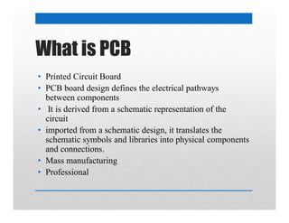
- 1. What is PCB • Printed Circuit Board • PCB board design defines the electrical pathways between components • It is derived from a schematic representation of the circuit • imported from a schematic design, it translates the schematic symbols and libraries into physical components and connections. • Mass manufacturing • Professional
- 2. Materials of PCB • Conducting layers are typically made of thin copper foil. • The board is typically coated with a solder mask that is green in color. Other colors that are normally available are blue and red. • Unwanted copper is removed from the substrate after etching leaving only the desired copper routes or pathways
- 3. Parts of PCB • Components • Pads • Routes • Vias • Top Metal Layer • Bottom Metal Layer
- 4. Manufacturing process 1. Film generation. 2. Shear raw material. 3. Apply image (toner transfer, photosensitive, silkscreen Or CNC). 4. Strip & etch. 5. Solder mask 6. Silkscreen overlay 7. drilling. 8. Soldering.
- 5. Design layers • A PCB design package allows the designer to define and design on multiple layers • Many of these are physical layers such as: • top layer. • Bottom layer • And some are special layers such as: • Solder & Paste Mask Layers • Silkscreen or Top Overlay Layers • Drill guides