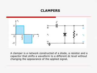
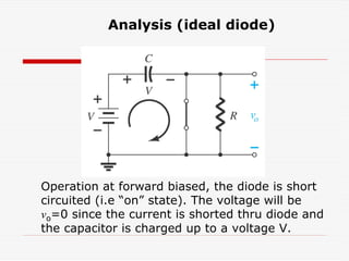
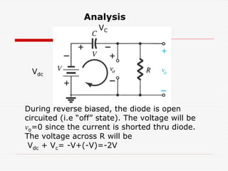
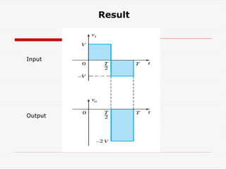
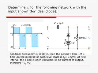
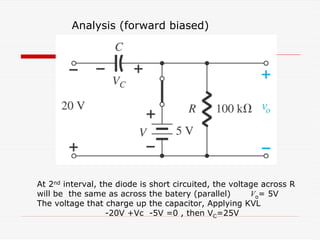
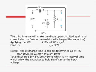
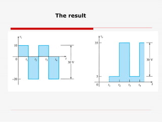
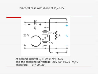
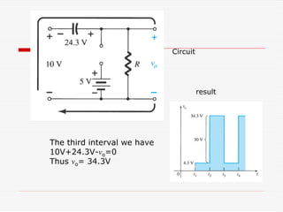
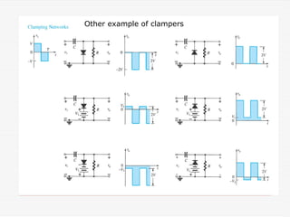
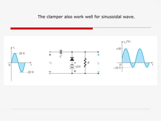
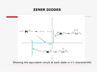
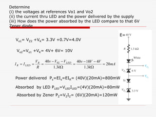
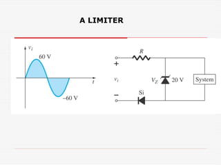
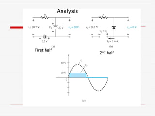
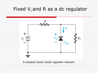
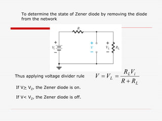
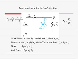
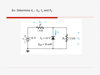
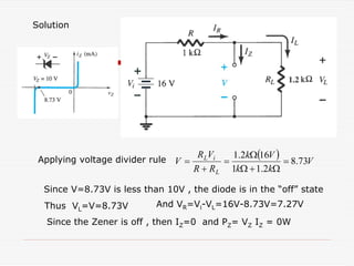
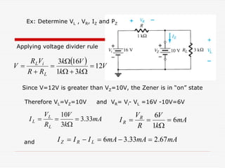
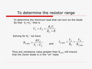
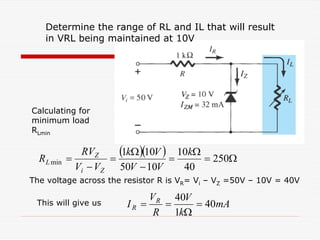
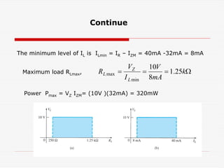
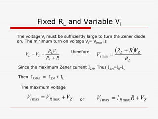
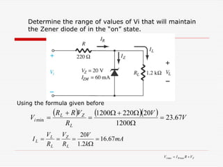
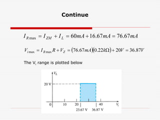
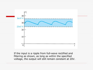
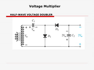
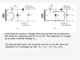
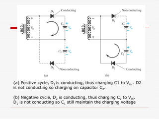
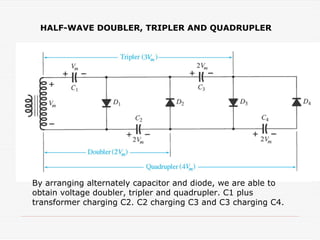
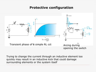
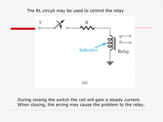
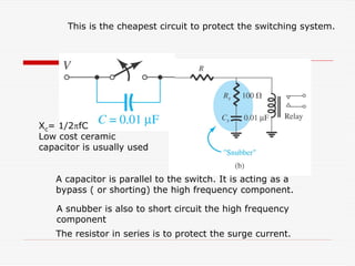
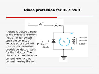
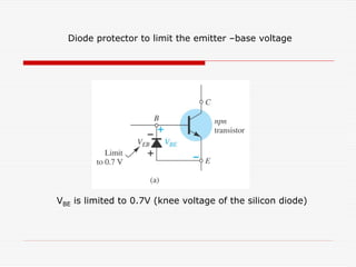
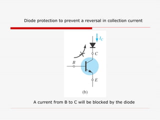
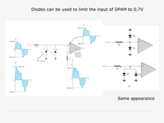
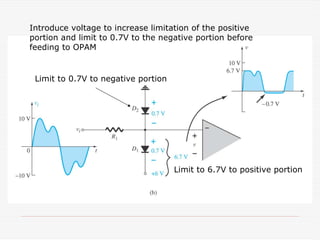
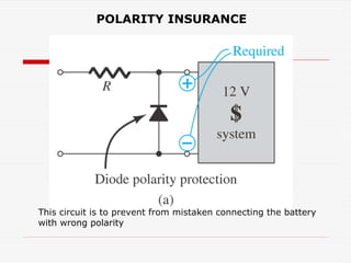
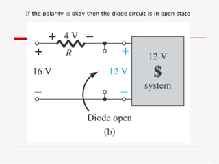
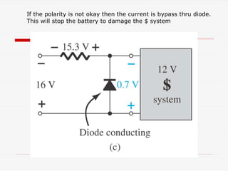
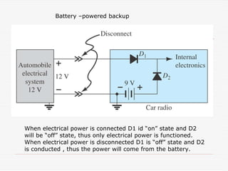
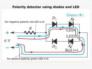
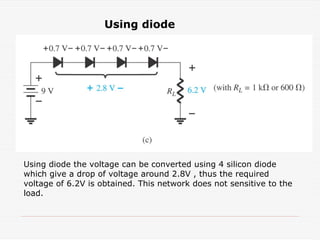
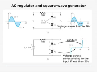
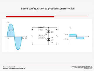
CLAMPERS
A clamper is a network constructed of a diode, a resistor and a
capacitor that shifts a waveform to a different dc level without
changing the appearance of the applied signal.
Operation at forward biased, the diode is short
circuited (i.e “on” state). The voltage will be
vo=0 since the current is shorted thru diode and
the capacitor is charged up to a voltage V.
Analysis (ideal diode)
Analysis
During reverse biased, the diode is open
circuited (i.e “off” state). The voltage will be
vo=0 since the current is shorted thru diode.
The voltage across R will be
Vdc + Vc= -V+(-V)=-2V
Vdc
VC
Result
Input
Output
Determine vo for the following network with the
input shown (for ideal diode).
Solution: Frequency is 1000Hz, then the period will be 1/f =
1ms ,so the interval for each level state is t1= 0.5ms. At first
interval the diode is open circuited, so no current at output,
therefore vo =0
Analysis (forward biased)
At 2nd interval, the diode is short circuited, the voltage across R
will be the same as across the batery (parallel) Vo= 5V
The voltage that charge up the capacitor, Applying KVL
-20V +Vc -5V =0 , then VC=25V
The third interval will make the diode open circuited again and
current start to flow in the resistor (discharged the capacitor).
Applying the KVL +10V +25V – vo=0
Give us vo= 35V
Noted : the discharge time is can be determined as t= RC
RC=100kΩ x 0.1mF= 0.01s= 10ms
Total discharge 5t= 5x10ms=50ms which is >>interval time
which allow the capacitor to hold significantly the input
voltage.
The result
Practical case with diode of Vk=0.7V
At second interval vo = 5V-0.7V= 4.3V
and the charging up voltage -20V-5V +0.7V+Vc=0
Therefore Vc= 24.3V
The third interval we have
10V+24.3V-vo=0
Thus vo= 34.3V
Circuit
result
Other example of clampers
The clamper also work well for sinusoidal wave.
ZENER DIODES
Showing the equivalent circuit at each state in V-I characteristic
Determine
(i) the voltages at references Vo1 and Vo2
(ii) the current thru LED and the power delivered by the supply
(iii) How does the power absorbed by the LED compare to that 6V
Zener diode
Vo1= VZ2 +VK= 3.3V +0.7V=4.0V
Vo2=Vo1 +VK= 4V+ 6V= 10V
mA
k
V
V
v
k
V
V
v
R
V
I
I LED
R
LED
R 20
3
.
1
4
10
40
3
.
1
40 02
=
Ω
−
−
=
Ω
−
−
=
=
=
Power delivered Ps=EIs=EIR= (40V)(20mA)=800mW
E=
Absorbed by LED PLED=VLEDILED=(4V)(20mA)=80mW
Absorbed by Zener PZ=VZIZ= (6V)(20mA)=120mW
A LIMITER
Analysis
First half
2nd half
Fixed Vi and R as a dc regulator
A simplest Zener diode regulator network
To determine the state of Zener diode by removing the diode
from the network
Thus applying voltage divider rule
L
i
L
L
R
R
V
R
V
V
+
=
=
If V> VZ, the Zener diode is on.
If V< VZ, the Zener diode is off.
Zener equivalent for the “on” situation
Since Zener is directly parallel to RL , then VL=VZ
Zener current , applying Kirchoff’s current law IR = IZ + IL
Thus IZ = IR – IL
And Power PZ= VZ IZ
L
L
L
R
V
I =
R
V
V
R
V
I L
i
R
R
−
=
=
Ex: Determine VL , VR, IZ and PZ
Solution
( ) V
k
k
V
k
R
R
V
R
V
L
i
L
73
.
8
2
.
1
1
16
2
.
1
=
Ω
+
Ω
Ω
=
+
=
Applying voltage divider rule
Since V=8.73V is less than 10V , the diode is in the “off” state
Thus VL=V=8.73V And VR=Vi-VL=16V-8.73V=7.27V
Since the Zener is off , then IZ=0 and PZ= VZ IZ = 0W
Ex: Determine VL , VR, IZ and PZ
( ) V
k
k
V
k
R
R
V
R
V
L
i
L
12
3
1
16
3
=
Ω
+
Ω
Ω
=
+
=
mA
mA
mA
I
I
I L
R
Z 67
.
2
33
.
3
6 =
−
=
−
=
mA
k
V
R
V
I
L
L
L 33
.
3
3
10
=
Ω
=
=
Applying voltage divider rule
Since V=12V is greater than VZ=10V, the Zener is in “on” state
Therefore VL=VZ=10V and VR= Vi- VL =16V -10V=6V
mA
k
V
R
V
I R
R 6
1
6
=
Ω
=
=
and
To determine the resistor range
Z
i
Z
L
V
V
RV
R
−
=
min
R
R
V
R
V
V
L
i
L
Z
L
+
=
=
min
min
L
Z
L
L
L
R
V
R
V
I =
=
To determine the minimum load that can turn on the diode
So that VL=VZ ‘ that is
Solving for RL ‘ we have
and
Thus any resistance value greater than RLmin will ensure
that the Zener diode is in the “on” state
To determine the resistor range
R
V
I R
R =
min
min
L
Z
L
I
V
R =
Once the diode is in the “on” state, the voltage across R
remains fixed at
VR= Vi - VZ
And IR remains fixed at
The Zener current IZ = IR - IL
But the IZ is limited by the manufacturer IZM , then
ILmin = IR - IZM
And the maximum load resistance as
mA
k
V
R
V
I R
R 40
1
40
=
Ω
=
=
( )( ) Ω
=
Ω
=
−
Ω
=
−
= 250
40
10
10
50
10
1
min
k
V
V
V
k
V
V
RV
R
Z
i
Z
L
The voltage across the resistor R is VR= Vi – VZ =50V – 10V = 40V
Determine the range of RL and IL that will result
in VRL being maintained at 10V
Calculating for
minimum load
RLmin
This will give us
Ω
=
=
= k
mA
V
I
V
R
L
Z
L 25
.
1
8
10
min
max
The minimum level of IL is ILmin = IR – IZM = 40mA -32mA = 8mA
Maximum load RLmax,
Continue
Power Pmax = VZ IZM= (10V )(32mA) = 320mW
Fixed RL and Variable Vi
R
R
V
R
V
V
L
i
L
Z
L
+
=
=
( )
L
Z
L
i
R
V
R
R
V
+
=
min
Z
R
i V
V
V +
= max
max Z
R
i V
R
I
V +
= max
max
The voltage Vi must be sufficiently large to turn the Zener diode
on. The minimum turn on voltage Vi= Vimin is
therefore
Since the maximum Zener current IZM, Thus IZM=IR-IL
Then IRMAX = IZM + IL
The maximum voltage
or
Determine the range of values of Vi that will maintain
the Zener diode of in the “on” state.
( ) ( )( ) V
V
R
V
R
R
V
L
Z
L
i 67
.
23
1200
20
220
1200
min =
Ω
Ω
+
Ω
=
+
=
mA
k
V
R
V
R
V
I
L
Z
L
L
L 67
.
16
2
.
1
20
=
Ω
=
=
=
Z
R
i V
R
I
V +
= max
max
Using the formula given before
mA
mA
mA
I
I
I L
ZM
R 67
.
76
67
.
16
60
max =
+
=
+
=
( )( ) V
V
k
mA
V
R
I
V Z
R
i 87
.
36
20
22
.
0
67
.
76
max
max =
+
Ω
=
+
=
Continue
The Vi range is plotted below
If the input is a ripple from full-wave rectified and
filtering as shown, as long as within the specified
voltage, the output will still remain constant at 20V.
Voltage Multiplier
HALF-WAVE VOLTAGE DOUBLER
(b) Second half cycle, D2 conducts and D1 is cut-off. Now the
capacitor C2 is charged up with Vm + VC = Vm +Vm=2Vm
(a)During the positive voltage half-cycle across the transformer,
the diode D1 conducts and D2 is cut off. The capacitor C1 charge
up to peak rectified voltage Vm .
VC
VC
FULL-WAVE VOLTAGE DOUBLER
(a) Positive cycle, D1 is conducting, thus charging C1 to Vm . D2
is not conducting so charging on capacitor C2.
(b) Negative cycle, D2 is conducting, thus charging C2 to Vm.
D1 is not conducting so C1 still maintain the charging voltage
HALF-WAVE DOUBLER, TRIPLER AND QUADRUPLER
By arranging alternately capacitor and diode, we are able to
obtain voltage doubler, tripler and quadrupler. C1 plus
transformer charging C2. C2 charging C3 and C3 charging C4.
Protective configuration
Trying to change the current through an inductive element too
quickly may result in an inductive kick that could damage
surrounding elements or the system itself
Transient phase of a simple RL cct Arcing during
opening the switch
The RL circuit may be used to control the relay
During closing the switch the coil will gain a steady current.
When closing, the arcing may cause the problem to the relay.
This is the cheapest circuit to protect the switching system.
A capacitor is parallel to the switch. It is acting as a
bypass ( or shorting) the high frequency component.
Xc= 1/2πfC
Low cost ceramic
capacitor is usually used
A snubber is also to short circuit the high frequency
component
The resistor in series is to protect the surge current.
Diode protection for RL circuit
A diode is placed parallel
to the inductive element
(relay). When switch
open the polarity of
voltage across coil will
turn on the diode thus
provide conduction path
for the inductor. The
diode must has the same
current level to that
current passing the coil
Diode protector to limit the emitter –base voltage
VBE is limited to 0.7V (knee voltage of the silicon diode)
Diode protection to prevent a reversal in collection current
A current from B to C will be blocked by the diode
Diodes can be used to limit the input of OPAM to 0.7V
Same appearance
Introduce voltage to increase limitation of the positive
portion and limit to 0.7V to the negative portion before
feeding to OPAM
Limit to 6.7V to positive portion
Limit to 0.7V to negative portion
POLARITY INSURANCE
This circuit is to prevent from mistaken connecting the battery
with wrong polarity
If the polarity is okay then the diode circuit is in open state
If the polarity is not okay then the current is bypass thru diode.
This will stop the battery to damage the $ system
Battery –powered backup
When electrical power is connected D1 id “on” state and D2
will be “off” state, thus only electrical power is functioned.
When electrical power is disconnected D1 is “off” state and D2
is conducted , thus the power will come from the battery.
Polarity detector using diodes and LED
For positive polarity green LED is lit
For negative polarity red LED is lit
LED diodes are arranged for EXIT sign display.
Voltage Reference Levels circuit
This circuit provide
different reference
levels
To establish a voltage level insensitive to the load current
A battery is connected to a network that has different
voltage supply and variable load. The battery available is
9V but the network require 6V. How?
Using external resistor
Let’s say the load is 1kΩ , then using voltage divider ,we determine
the value of external resistor we obtain approximately 470Ω
We calculate the VRL , give us 6.1V
Now if we change the load to 600 W but the external still same ,
then VRL become 4.9V … thus the system will not operate correctly!!
Using diode
Using diode the voltage can be converted using 4 silicon diode
which give a drop of voltage around 2.8V , thus the required
voltage of 6.2V is obtained. This network does not sensitive to the
load.
AC regulator and square-wave generator
conduct
Voltage across
corresponding to the
input if less than 20V
Voltage across limit to 20V
Robert L. Boylestad
Electronic Devices and Circuit Theory, 9e
Copyright ©2006 by Pearson Education, Inc.
Upper Saddle River, New Jersey 07458
All rights reserved.
Same configuration to produce square -wave

Electronic device lecture-4 B.Tech Semester-3.pdf

  • 1.
    CLAMPERS A clamper isa network constructed of a diode, a resistor and a capacitor that shifts a waveform to a different dc level without changing the appearance of the applied signal.
  • 2.
    Operation at forwardbiased, the diode is short circuited (i.e “on” state). The voltage will be vo=0 since the current is shorted thru diode and the capacitor is charged up to a voltage V. Analysis (ideal diode)
  • 3.
    Analysis During reverse biased,the diode is open circuited (i.e “off” state). The voltage will be vo=0 since the current is shorted thru diode. The voltage across R will be Vdc + Vc= -V+(-V)=-2V Vdc VC
  • 4.
  • 5.
    Determine vo forthe following network with the input shown (for ideal diode). Solution: Frequency is 1000Hz, then the period will be 1/f = 1ms ,so the interval for each level state is t1= 0.5ms. At first interval the diode is open circuited, so no current at output, therefore vo =0
  • 6.
    Analysis (forward biased) At2nd interval, the diode is short circuited, the voltage across R will be the same as across the batery (parallel) Vo= 5V The voltage that charge up the capacitor, Applying KVL -20V +Vc -5V =0 , then VC=25V
  • 7.
    The third intervalwill make the diode open circuited again and current start to flow in the resistor (discharged the capacitor). Applying the KVL +10V +25V – vo=0 Give us vo= 35V Noted : the discharge time is can be determined as t= RC RC=100kΩ x 0.1mF= 0.01s= 10ms Total discharge 5t= 5x10ms=50ms which is >>interval time which allow the capacitor to hold significantly the input voltage.
  • 8.
  • 9.
    Practical case withdiode of Vk=0.7V At second interval vo = 5V-0.7V= 4.3V and the charging up voltage -20V-5V +0.7V+Vc=0 Therefore Vc= 24.3V
  • 10.
    The third intervalwe have 10V+24.3V-vo=0 Thus vo= 34.3V Circuit result
  • 11.
  • 12.
    The clamper alsowork well for sinusoidal wave.
  • 13.
    ZENER DIODES Showing theequivalent circuit at each state in V-I characteristic
  • 14.
    Determine (i) the voltagesat references Vo1 and Vo2 (ii) the current thru LED and the power delivered by the supply (iii) How does the power absorbed by the LED compare to that 6V Zener diode Vo1= VZ2 +VK= 3.3V +0.7V=4.0V Vo2=Vo1 +VK= 4V+ 6V= 10V mA k V V v k V V v R V I I LED R LED R 20 3 . 1 4 10 40 3 . 1 40 02 = Ω − − = Ω − − = = = Power delivered Ps=EIs=EIR= (40V)(20mA)=800mW E= Absorbed by LED PLED=VLEDILED=(4V)(20mA)=80mW Absorbed by Zener PZ=VZIZ= (6V)(20mA)=120mW
  • 15.
  • 16.
  • 17.
    Fixed Vi andR as a dc regulator A simplest Zener diode regulator network
  • 18.
    To determine thestate of Zener diode by removing the diode from the network Thus applying voltage divider rule L i L L R R V R V V + = = If V> VZ, the Zener diode is on. If V< VZ, the Zener diode is off.
  • 19.
    Zener equivalent forthe “on” situation Since Zener is directly parallel to RL , then VL=VZ Zener current , applying Kirchoff’s current law IR = IZ + IL Thus IZ = IR – IL And Power PZ= VZ IZ L L L R V I = R V V R V I L i R R − = =
  • 20.
    Ex: Determine VL, VR, IZ and PZ
  • 21.
    Solution ( ) V k k V k R R V R V L i L 73 . 8 2 . 1 1 16 2 . 1 = Ω + Ω Ω = + = Applyingvoltage divider rule Since V=8.73V is less than 10V , the diode is in the “off” state Thus VL=V=8.73V And VR=Vi-VL=16V-8.73V=7.27V Since the Zener is off , then IZ=0 and PZ= VZ IZ = 0W
  • 22.
    Ex: Determine VL, VR, IZ and PZ ( ) V k k V k R R V R V L i L 12 3 1 16 3 = Ω + Ω Ω = + = mA mA mA I I I L R Z 67 . 2 33 . 3 6 = − = − = mA k V R V I L L L 33 . 3 3 10 = Ω = = Applying voltage divider rule Since V=12V is greater than VZ=10V, the Zener is in “on” state Therefore VL=VZ=10V and VR= Vi- VL =16V -10V=6V mA k V R V I R R 6 1 6 = Ω = = and
  • 23.
    To determine theresistor range Z i Z L V V RV R − = min R R V R V V L i L Z L + = = min min L Z L L L R V R V I = = To determine the minimum load that can turn on the diode So that VL=VZ ‘ that is Solving for RL ‘ we have and Thus any resistance value greater than RLmin will ensure that the Zener diode is in the “on” state
  • 24.
    To determine theresistor range R V I R R = min min L Z L I V R = Once the diode is in the “on” state, the voltage across R remains fixed at VR= Vi - VZ And IR remains fixed at The Zener current IZ = IR - IL But the IZ is limited by the manufacturer IZM , then ILmin = IR - IZM And the maximum load resistance as
  • 25.
    mA k V R V I R R 40 1 40 = Ω = = ()( ) Ω = Ω = − Ω = − = 250 40 10 10 50 10 1 min k V V V k V V RV R Z i Z L The voltage across the resistor R is VR= Vi – VZ =50V – 10V = 40V Determine the range of RL and IL that will result in VRL being maintained at 10V Calculating for minimum load RLmin This will give us
  • 26.
    Ω = = = k mA V I V R L Z L 25 . 1 8 10 min max Theminimum level of IL is ILmin = IR – IZM = 40mA -32mA = 8mA Maximum load RLmax, Continue Power Pmax = VZ IZM= (10V )(32mA) = 320mW
  • 27.
    Fixed RL andVariable Vi R R V R V V L i L Z L + = = ( ) L Z L i R V R R V + = min Z R i V V V + = max max Z R i V R I V + = max max The voltage Vi must be sufficiently large to turn the Zener diode on. The minimum turn on voltage Vi= Vimin is therefore Since the maximum Zener current IZM, Thus IZM=IR-IL Then IRMAX = IZM + IL The maximum voltage or
  • 28.
    Determine the rangeof values of Vi that will maintain the Zener diode of in the “on” state. ( ) ( )( ) V V R V R R V L Z L i 67 . 23 1200 20 220 1200 min = Ω Ω + Ω = + = mA k V R V R V I L Z L L L 67 . 16 2 . 1 20 = Ω = = = Z R i V R I V + = max max Using the formula given before
  • 29.
    mA mA mA I I I L ZM R 67 . 76 67 . 16 60 max= + = + = ( )( ) V V k mA V R I V Z R i 87 . 36 20 22 . 0 67 . 76 max max = + Ω = + = Continue The Vi range is plotted below
  • 30.
    If the inputis a ripple from full-wave rectified and filtering as shown, as long as within the specified voltage, the output will still remain constant at 20V.
  • 31.
  • 32.
    (b) Second halfcycle, D2 conducts and D1 is cut-off. Now the capacitor C2 is charged up with Vm + VC = Vm +Vm=2Vm (a)During the positive voltage half-cycle across the transformer, the diode D1 conducts and D2 is cut off. The capacitor C1 charge up to peak rectified voltage Vm . VC VC
  • 33.
  • 34.
    (a) Positive cycle,D1 is conducting, thus charging C1 to Vm . D2 is not conducting so charging on capacitor C2. (b) Negative cycle, D2 is conducting, thus charging C2 to Vm. D1 is not conducting so C1 still maintain the charging voltage
  • 35.
    HALF-WAVE DOUBLER, TRIPLERAND QUADRUPLER By arranging alternately capacitor and diode, we are able to obtain voltage doubler, tripler and quadrupler. C1 plus transformer charging C2. C2 charging C3 and C3 charging C4.
  • 36.
    Protective configuration Trying tochange the current through an inductive element too quickly may result in an inductive kick that could damage surrounding elements or the system itself Transient phase of a simple RL cct Arcing during opening the switch
  • 37.
    The RL circuitmay be used to control the relay During closing the switch the coil will gain a steady current. When closing, the arcing may cause the problem to the relay.
  • 38.
    This is thecheapest circuit to protect the switching system. A capacitor is parallel to the switch. It is acting as a bypass ( or shorting) the high frequency component. Xc= 1/2πfC Low cost ceramic capacitor is usually used A snubber is also to short circuit the high frequency component The resistor in series is to protect the surge current.
  • 39.
    Diode protection forRL circuit A diode is placed parallel to the inductive element (relay). When switch open the polarity of voltage across coil will turn on the diode thus provide conduction path for the inductor. The diode must has the same current level to that current passing the coil
  • 40.
    Diode protector tolimit the emitter –base voltage VBE is limited to 0.7V (knee voltage of the silicon diode)
  • 41.
    Diode protection toprevent a reversal in collection current A current from B to C will be blocked by the diode
  • 42.
    Diodes can beused to limit the input of OPAM to 0.7V Same appearance
  • 43.
    Introduce voltage toincrease limitation of the positive portion and limit to 0.7V to the negative portion before feeding to OPAM Limit to 6.7V to positive portion Limit to 0.7V to negative portion
  • 44.
    POLARITY INSURANCE This circuitis to prevent from mistaken connecting the battery with wrong polarity
  • 45.
    If the polarityis okay then the diode circuit is in open state
  • 46.
    If the polarityis not okay then the current is bypass thru diode. This will stop the battery to damage the $ system
  • 47.
    Battery –powered backup Whenelectrical power is connected D1 id “on” state and D2 will be “off” state, thus only electrical power is functioned. When electrical power is disconnected D1 is “off” state and D2 is conducted , thus the power will come from the battery.
  • 48.
    Polarity detector usingdiodes and LED For positive polarity green LED is lit For negative polarity red LED is lit
  • 49.
    LED diodes arearranged for EXIT sign display.
  • 50.
    Voltage Reference Levelscircuit This circuit provide different reference levels
  • 51.
    To establish avoltage level insensitive to the load current A battery is connected to a network that has different voltage supply and variable load. The battery available is 9V but the network require 6V. How?
  • 52.
    Using external resistor Let’ssay the load is 1kΩ , then using voltage divider ,we determine the value of external resistor we obtain approximately 470Ω We calculate the VRL , give us 6.1V Now if we change the load to 600 W but the external still same , then VRL become 4.9V … thus the system will not operate correctly!!
  • 53.
    Using diode Using diodethe voltage can be converted using 4 silicon diode which give a drop of voltage around 2.8V , thus the required voltage of 6.2V is obtained. This network does not sensitive to the load.
  • 54.
    AC regulator andsquare-wave generator conduct Voltage across corresponding to the input if less than 20V Voltage across limit to 20V
  • 55.
    Robert L. Boylestad ElectronicDevices and Circuit Theory, 9e Copyright ©2006 by Pearson Education, Inc. Upper Saddle River, New Jersey 07458 All rights reserved. Same configuration to produce square -wave