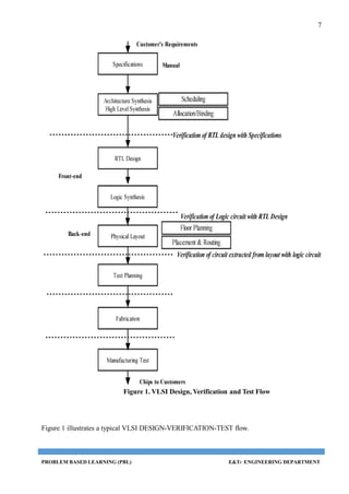
1. The document describes a VLSI design flow for a digital integrated circuit from specification to logic synthesis. It uses a 4-bit ripple carry adder example to explain the steps.
2. The steps are: specification, high-level synthesis to RTL, logic synthesis to gates, and backend physical design. High-level synthesis schedules operations and binds variables and operations to hardware units like adders and registers.
3. Logic synthesis derives Boolean equations from the RTL and implements them with logic gates. Equivalence checking is done between each step and the original specification.
![5
PROBLEM BASED LEARNING (PBL) E&TC ENGINEERING DEPARTMENT
VLSI DESIGN
The functionality of electronics equipments and gadgets has achieved a phenomenal
growth over the last two decades while their physical sizes and weights have come down
drastically. The major reason is due to the rapid advances in integration technologies, which
enables fabrication of millions of transistors in a single Integrated Circuit (IC) or chip. IC (used
interchangeably with “chip” in this lecture) is a device having multiple transistors with
interconnects manufactured on a single silicon substrate. Integration with a complexity of 10's of
transistors is called Small Scale Integration, with 100's is Medium Scale Integration (MSI), with
1000's is Large Scale Integration (LSI), with 10,000 it is Very Large Scale Integration (VLSI) [1].
As a very huge number of components can be integrated in a single IC fabricated using VLSI
technology, the variant of functionalities provided by such ICs can be as large as those which were
provided by thousands of LSI ICs. In other words, systems can be implemented in a VLSI IC.
However, with this rise in functionality of VLSI ICs, design problem has become more challenging
and complex. To address this complexly issue, post design steps are automated using Computer
Aided Design (CAD) tools. However, even designs using automated CAD tools may have bugs.
Also, due to extremely large size of the design space it is not possible to verify correctness of the
design under all possible situations. So techniques are required that can verify, without exercising
exhaustive input-output combinations, that the design meets all the input specifications; this
technique is called formal verification. Finally, when the design meets all specifications (as it is
formally verified) it is manufactured and sent to market. In VLSI designs as millions of transistors
are packed into a single chip, the device and interconnect sizes are extremely small and so are the
inter-component distances. This may lead to manufacturing defects and all the chips need to be
physically tested by giving input signals from a pattern generator and comparing responses using a
logic analyzer; this process is called testing. So, in the process of manufacturing a VLSI IC there
are three broad steps: DESIGN-VERIFICATION-TEST. There are algorithms and CAD tools
which automate these three steps.
VLSI ICs can be divided into analog, digital or mixed-signal (both analog and
digital on the same chip) based on their functionality. Digital ICs can contain logic gates, flip-flops,
multiplexers, and other circuits which work using binary mathematics to process "one" and "zero"](https://image.slidesharecdn.com/gourp12report-230712161816-db764852/85/Gourp-12-Report-pptx-5-320.jpg)
![6
signals. Analog ICs, such as current mirrors, voltage followers, filters, OPAMPs etc. work by
processing continuous signals. They perform functions like amplification, active filtering,
demodulation etc. When single IC has both analog and digital components it is called mixed signal
IC e.g, Analog to Digital Converter (ADC). The automation algorithms and CAD tools are mainly
available for digital ICs because digital circuits comprise millions of components and
transformation of design specifications to silicon implementation can be accomplished using
logical procedures (which can be converted to algorithms and tools) [2]. However, most of the
analog circuits comprise less than hundred devices and its design is like an “art” which is best
performed by designers with “aid” of some CAD tools (which provides feedback to designer if the
manual design is progressing fine etc.) [2]. In this course we will deal only with digital VLSI
circuits. Henceforth, in this course VLSI IC would imply digital VLSI ICs only and whenever we
want to discuss about analog or mixed signal ICs it will be mentioned explicitly. Also, in this
course the terms ICs and chips would mean VLSI ICs and chips
PROBLEM BASED LEARNING (PBL) E&TC ENGINEERING DEPARTMENT](https://image.slidesharecdn.com/gourp12report-230712161816-db764852/85/Gourp-12-Report-pptx-6-320.jpg)
![8
PROBLEM BASED LEARNING (PBL) E&TC ENGINEERING DEPARTMENT
Step1: Specification Design
In a typical VLSI flow, we start with system specifications, which is nothing but
technical representation of design intent. To explain the flow, the following example will be used
through this section.
Example:
Specification: out1=a+b; out2=c+d; where a,b,c,d are single bit inputs and out1,out2 are two bit
outputs (sum and carry).
Step 2: High level Synthesis
High-Level Synthesis (HLS) algorithms are used to convert specifications into Register
Transfer Level (RTL) circuits.
HLS, sometimes referred to as architectural synthesis is an automated design procedure
that interprets an algorithmic description of the design intent and creates hardware at RTL that
implements that behavior [3]. The input to a HLS tool is design intent written in some high level
hardware definition language like SystemC, System Verilog etc. The HLS tool first schedules the
computations (required to meet the specifications) at different control steps. The computations
scheduled at each control step contains operations which can be performed in a single clock cycle
in the hardware. Following that, depending on availability of hardware units and time constraints,
the scheduled computations (comprising instructions and variables) are allocated and binded to the
hardware units like adders, multipliers, multiplexors, registers, wires etc.
Example:
In the example there are two operations (addition of single bit numbers) and none of
them depend on each other. So both the operations can be scheduled in a single control step.
However, if there are dependencies e.g., out1=a+b; out2=out1+d; then “out1=a+b;” is scheduled in](https://image.slidesharecdn.com/gourp12report-230712161816-db764852/85/Gourp-12-Report-pptx-8-320.jpg)

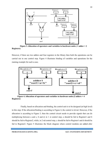
![11
allocation and binding (Figure 3). It may be noted that control signal is not available as an external
pin which can be controlled by the user. “ Control” is connected to some signal generated by the
system, which alternates in every control step thereby making its value 0 in 1 st step and 1 in the 2
nd .
Figure 5. Block diagram with control modules added after allocation and binding
The HLS tool generates output comprising, (i) operations-variables allocated-binded to
hardware units and (ii) control modules. The output of HLS tool is called Register Transfer Level
(RTL) circuit because data flow, data operations and control flow are captured between registers.
After HLS, RTL circuits are transformed into logic gate level implementation; the step is called
logic synthesis.
Before the starting of logic synthesis, one needs to verify if the RTL is equivalent to the
specifications. In the running example, we can verify by applying all possible input conditions of
a,b,c,d (along with control , if RTL is as per Figure 5) to the RTL and checking if out1 and out2 are
as expected. However, if the RTL has about hundreds of inputs then exercising all possible inputs
is impossible because of the exponential complexity (i.e., if there are n inputs then all
possible input combinations are 2n). So we need to have formal verification methods which verify
equivalence of RTL with input specifications. Broadly speaking, for formal verification we need to
model the RTL circuit and the specifications using some formal modeling techniques and verify
that both of them are equivalent. In other words, equivalence is determined without applying
inputs. Figure 6 illustrates Control and Data Flow Diagram (CDFG) [4], a formal modeling, to
capture the RTL of Figure 5.In Figure 7 we illustrate a Finite State Machine (FSM) [4] to model
the control logic of the RTL of Figure 5.This example being very simple, we can see that both
PROBLEM BASED LEARNING (PBL) E&TC ENGINEERING DEPARTMENT](https://image.slidesharecdn.com/gourp12report-230712161816-db764852/85/Gourp-12-Report-pptx-11-320.jpg)
![12
specifications and the model are equivalent. Formal techniques for checking equivalence can be
found in [5] and will be elaborated in “VERIFICATION” section of the course.
Figure 6. CDFG of the RTLcircuit of Figure 5
Figure 7. FSM for the control logic of RTLcircuit shown in Figure
Step 3: Logic Synthesis
After the RTL is verified to be equivalent to system specification, logic synthesis is
performed by CAD tools. In logic synthesis all blocks of the RTL circuit is transformed into logic
gates and flip-flops. For the running example all the blocks namely, adder, multiplexers, control
logic etc. need to be synthesized to logic gates. Here, we will illustrate synthesis only for the adder
PROBLEM BASED LEARNING (PBL) E&TC ENGINEERING DEPARTMENT](https://image.slidesharecdn.com/gourp12report-230712161816-db764852/85/Gourp-12-Report-pptx-12-320.jpg)
![13
module and for the rest, similar procedure holds. We will discuss a typical procedure here in brief
and details will be explained in the “DESIGN” module of the course.
We first determine the Boolean function of the adder module, in terms of mean terms. Table 1
illustrates the input –output of the adder module.
Table 1. Input –output of the adder module
a b Out 1(sum) Out 1(carry)
0 0 0 0
0 1 1 0
1 0 1 0
1 1 0 1
From the table we have Boolean equations for
Out1(sum)= and Out1(carry)=ab
After the equations are obtained they need to be minimized so that the circuit can be
implemented using minimal number of gates. Karnaugh map, Quine–McCluskey algorithm etc. [6]
are some standard techniques to minimize Boolean functions. In this example of the adder, the
equations are already minimized and can be directly converted to Boolean gate implementation as
shown in Figure 8. Karnaugh map and Quine–McCluskey techniques work well if the number of
inputs is less. However, in case of practical VLSI circuits the number of inputs are in orders of
hundreds, so minimization is carried out using heuristics techniques, which will be discussed in the
“DESIGN” module of the course.
Again equivalence of logic synthesis output should be established with RTL design.
Figure 8. Circuit after logic synthesis for the adder block (of Figure 5)
PROBLEM BASED LEARNING (PBL) E&TC ENGINEERING DEPARTMENT](https://image.slidesharecdn.com/gourp12report-230712161816-db764852/85/Gourp-12-Report-pptx-13-320.jpg)
![14
PROBLEM BASED LEARNING (PBL) E&TC ENGINEERING DEPARTMENT
Step 4: Backend
Once the logic level output of the circuit is obtained we move to backend phase of the
design process. Broadly speaking, in backend we start with a software version of the silicon die
where the chip will be finally fabricated. In the process, we first make a broad plan regarding
placement of gates, flip-flops etc. (output of logic synthesis) in appropriate places in the software
representation of the chip; this process is called Floorplan. Following that, we decide on the exact
locations in the die (software representation) where the circuit components are placed; this is
called Placement. Once placement is done, we make the required interconnections (as given in the
logic circuit) among the gates that are placed in exact positions in the die; this process is called
Routing. The main aim of Floorplan, Placement and Routing is to minimize silicon area, minimize
signal delays, well distributed power flow etc., subject to accommodating all the components of
the chip and adhere to the design check rules [7].
In this course we will not discuss the Backend phase of design flow; for details the reader
is refereed to [7].
Again equivalence of output of Backend process should be established with logic design.
In this process we extract the logic circuit from the placed and routed circuit in the die (software
representation) and equivalence is verified against logic design (output of logic synthesis).
Step 5: Test Planning
As discussed, in VLSI designs millions of transistors are packed into a single chip, thereby
leading to manufacturing defects. So all chips need to be physically tested by providing input
signals from a pattern generator and comparing responses using a logic analyzer. As in the case of
verification, testing by applying all possible input combinations is prohibitive, due to curse of
dimensionality problem. The testing problem is more time hungry than verification because all
chips need to be tested while only “one” design is to be verified. Testing by applying all possible
input combinations is called exhaustive functional testing, which is avoided because of prohibitive
time requirements.](https://image.slidesharecdn.com/gourp12report-230712161816-db764852/85/Gourp-12-Report-pptx-14-320.jpg)
![15
Testing is therefore done based on “structure” of the circuit and is called structural testing.
In structural testing we first decide on set of faults that can occur, called Fault Models; stuck-at,
bridging etc. are some well known fault models. Then we apply only those inputs which are
required to validate that faults (as per fault model) are not present. It has been shown in [9] that
number of patterns required to perform structural testing is exponentially lower than that required
for exhaustive functional testing. In Test Planning step, given a logic level circuit and fault model,
we generate patterns, which when applied to a circuit determines that no fault from the fault model
exists in the circuit.
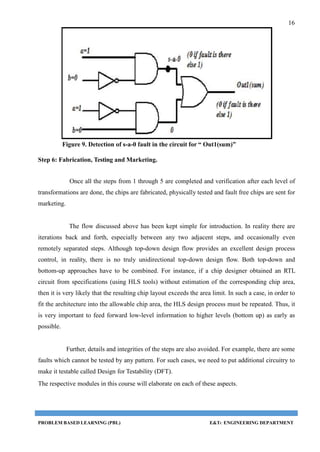
Now we will illustrate test planning for the adder module of the example (Figure 8)
assuming that fault model is “stuck-at”. In “stuck-at” fault model each line of the circuit is
assumed to have two types of faults i.e., stuck-at-0 and stuck-at-0. So if there are n lines in a circuit
then in all there can be 2n stuck-at faults in the circuit. However, in the fault model it is assumed
that only one stuck-at fault can occur at a time. In test planning we need to find input patterns
which can determine that none of the stuck-at faults are present. In the circuit of Figure 8 as there
are 12 lines (9 lines in circuit for “sum” and 3 lines in the circuit for “carry”), there can be 24
stuck-at faults. We take one fault at a time and determine an input pattern that can verify the
absence of the fault. Here we will illustrate for only one fault and the same holds for all the other
23 faults. Let there be a stuck-at-0 fault in the output of one AND gate (shown in Figure 9) of the
circuit for “sum”. Now to we need to find an input pattern that can verify the absence of the fault
i.e., when the pattern in applied the output under normal and fault cases are different. Form Figure
9 it may be noted that if a=1 and b=0 is applied as inputs, then “output1(sum)” is 0 if fault is
present, 1 otherwise. So a=1 and b=0 can verify the absence of fault by comparing output with 1.
It may be the fact that one pattern can test more than one fault and one fault can be tested
by more than one pattern. Broadly speaking, determination of minimal test patterns which cover all
faults is the most important step in test planning. Algorithms and techniques to perform test
planning will be covered in “TESTING” part of the course.
PROBLEM BASED LEARNING (PBL) E&TC ENGINEERING DEPARTMENT](https://image.slidesharecdn.com/gourp12report-230712161816-db764852/85/Gourp-12-Report-pptx-15-320.jpg)
![20
PROBLEM BASED LEARNING (PBL) E&TC ENGINEERING DEPARTMENT
References
1] John P. Uyemura, , “CMOS Logic Circuit Design”, Kluwer Academic Publishers, 1 st Edition,
1999.
2Stephen M. Trimberger, “Introduction to CAD for VLSI”, Kluwer Academic Publishers, 1 st
Edition, 1987.
3Daniel D. Gajski and Loganath Ramachandran, “Introduction to High-Level Synthesis”, IEEE
Design and. Test, volume 11,No, 4,1994, pp 44—54.
4 Daniel D. Gajski, Nikil D. Dutt, Allen C-H Wu, Steve Y-L Lin, “High-Level Synthesis:
Introduction to Chip and System Design”, Kluwer Academic Publishers, 1 st Edition, 1992
5Jr., Edmund M. Clarke, Orna Grumberg and Doron A Peled, “Model checking”, MIT
Press, 1 st Edition, 1999.
6Giovanni De Micheli, “Synthesis and Optimization of Digital Circuits”, McGraw-Hill Higher
Education, 1 st Edition, 1994.
7Naveed A. Sherwani, “Algorithms for VLSI Physical Design Automation”, Kluwer Academic
Publishers, 2 nd Edition, 1995.
8M. Abramovici, M.A. Breuer, and A.D. Friedman. Digital Systems Testing and Testable
Design. Wiley-IEEE Press, 1994.](https://image.slidesharecdn.com/gourp12report-230712161816-db764852/85/Gourp-12-Report-pptx-20-320.jpg)