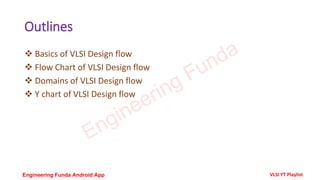
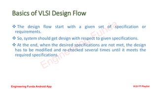
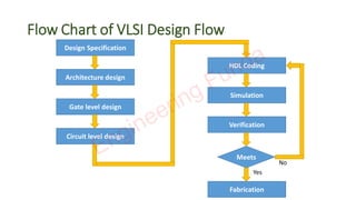
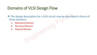
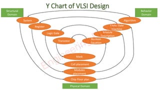
VLSI Design Flow
By Prof. Hitesh Dholakiya
Engineering Funda
VLSI Lecture series
Engineering Funda
Engineering Funda Android App VLSI YT Playlist
Outlines
❖ Basics of VLSI Design flow
❖ Flow Chart of VLSI Design flow
❖ Domains of VLSI Design flow
❖ Y chart of VLSI Design flow
Engineering Funda
Engineering Funda Android App VLSI YT Playlist
Basics of VLSI Design Flow
❖ The design flow start with a given set of specification or
requirements.
❖ So, system should get design with respect to given specifications.
❖ At the end, when the desired specifications are not met, the design
has to be modified and re-checked several times until it meets the
required specifications.
Engineering Funda
Engineering Funda Android App VLSI YT Playlist
Flow Chart of VLSI Design Flow
Design Specification
Architecture design
Gate level design
Circuit level design
HDL Coding
Simulation
Verification
Meets
Fabrication
Yes
No
Engineering Funda
Domains of VLSI Design Flow
❖ The design description for a VLSI circuit may be described in forms of
three domains:
1. Behavioral Domain
2. Structural Domain
3. Physical Domain
Engineering Funda
Y Chart of VLSI Design
Behavior
Domain
Structural
Domain
Physical Domain
Algorithm
System
Chip Floor plan
Finite State
Machine
Register
Modules
placement
Module
Description
Logic Gate
Cell placement
Boolean
Equation
Transistor
Mask
Engineering Funda

VLSI Design Flow

  • 1.
    VLSI Design Flow ByProf. Hitesh Dholakiya Engineering Funda VLSI Lecture series Engineering Funda Engineering Funda Android App VLSI YT Playlist
  • 2.
    Outlines ❖ Basics ofVLSI Design flow ❖ Flow Chart of VLSI Design flow ❖ Domains of VLSI Design flow ❖ Y chart of VLSI Design flow Engineering Funda Engineering Funda Android App VLSI YT Playlist
  • 3.
    Basics of VLSIDesign Flow ❖ The design flow start with a given set of specification or requirements. ❖ So, system should get design with respect to given specifications. ❖ At the end, when the desired specifications are not met, the design has to be modified and re-checked several times until it meets the required specifications. Engineering Funda Engineering Funda Android App VLSI YT Playlist
  • 4.
    Flow Chart ofVLSI Design Flow Design Specification Architecture design Gate level design Circuit level design HDL Coding Simulation Verification Meets Fabrication Yes No Engineering Funda
  • 5.
    Domains of VLSIDesign Flow ❖ The design description for a VLSI circuit may be described in forms of three domains: 1. Behavioral Domain 2. Structural Domain 3. Physical Domain Engineering Funda
  • 6.
    Y Chart ofVLSI Design Behavior Domain Structural Domain Physical Domain Algorithm System Chip Floor plan Finite State Machine Register Modules placement Module Description Logic Gate Cell placement Boolean Equation Transistor Mask Engineering Funda