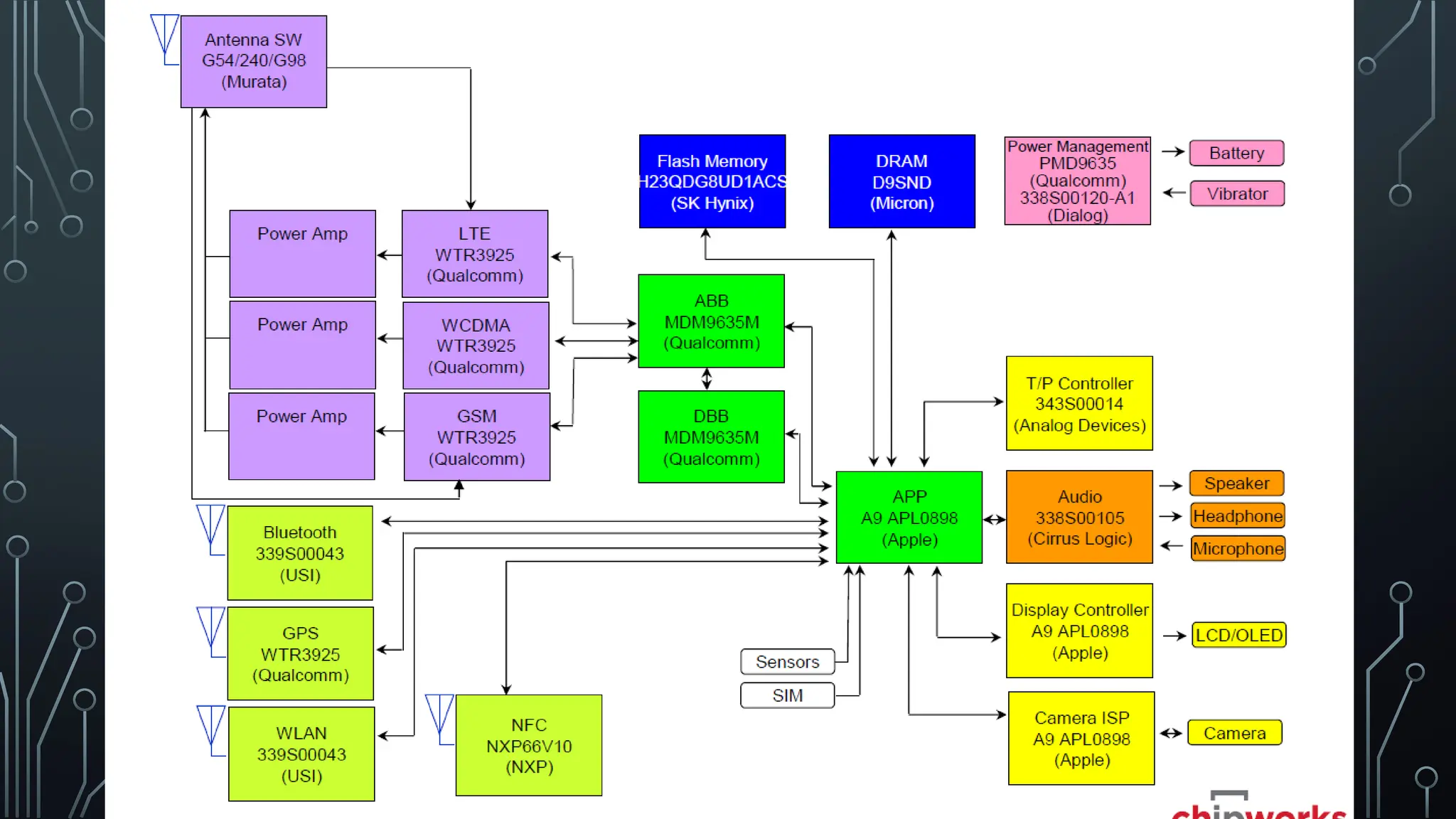
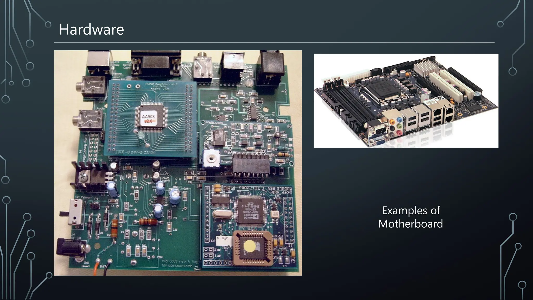
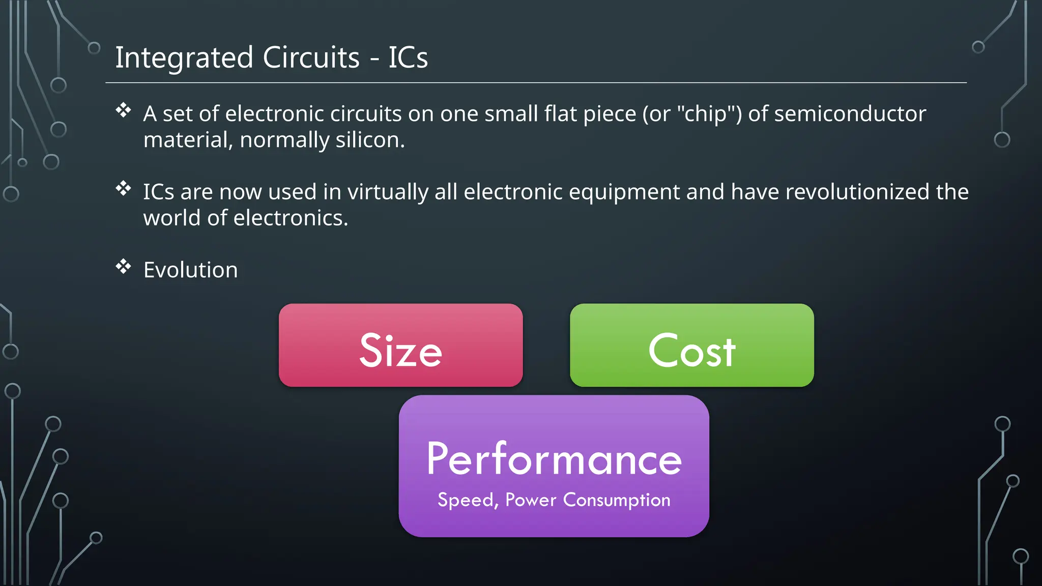
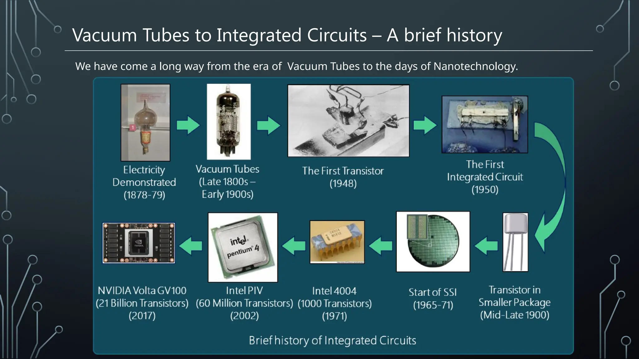
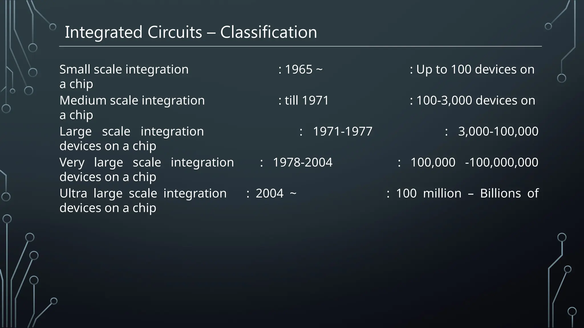
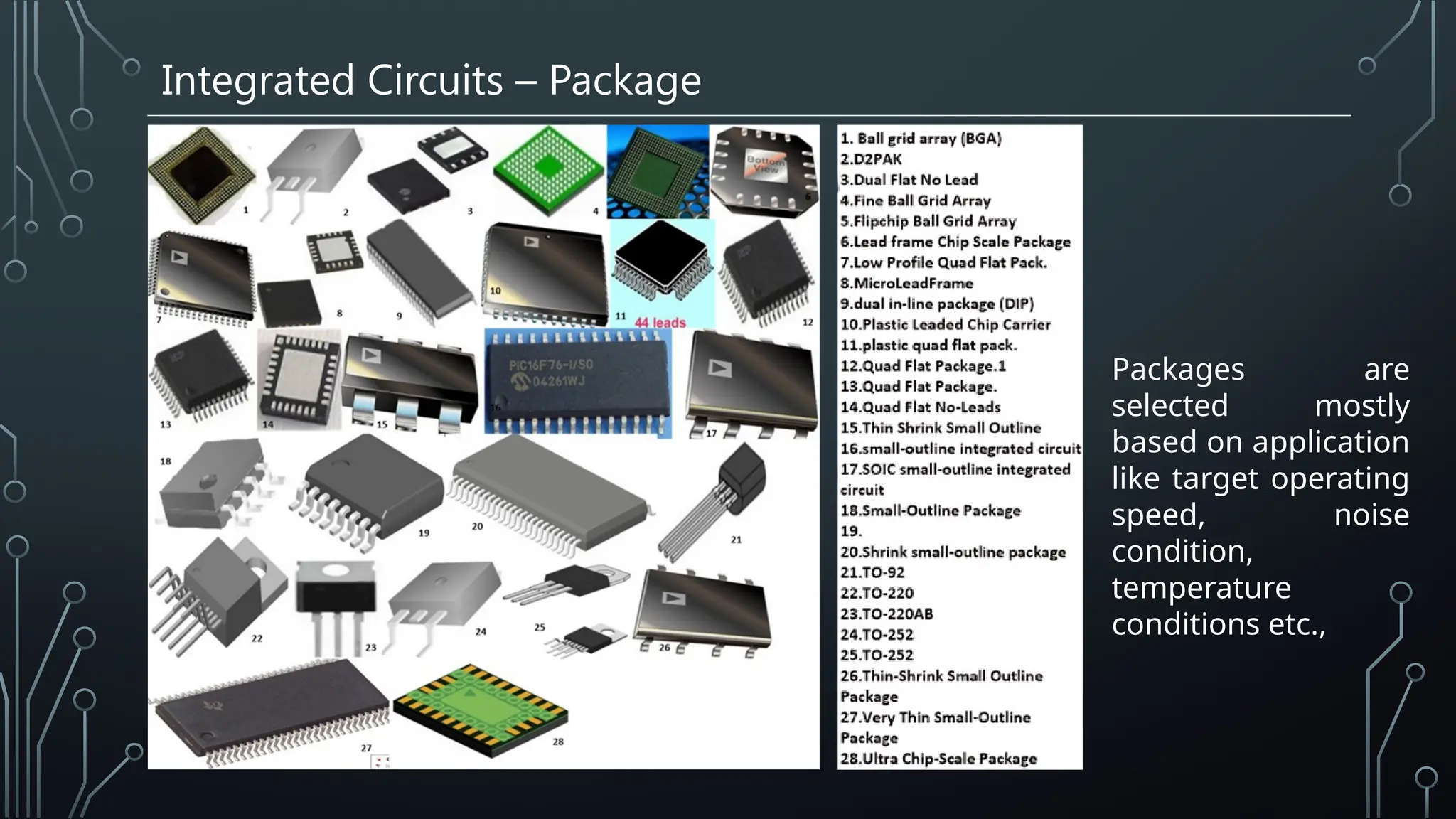
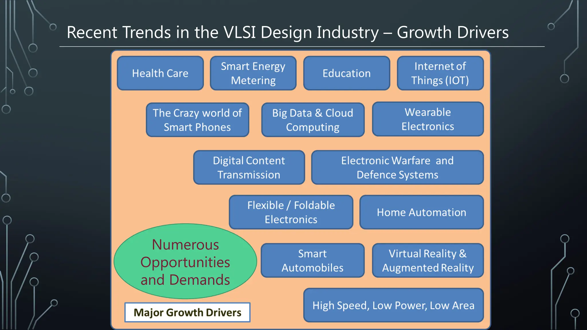
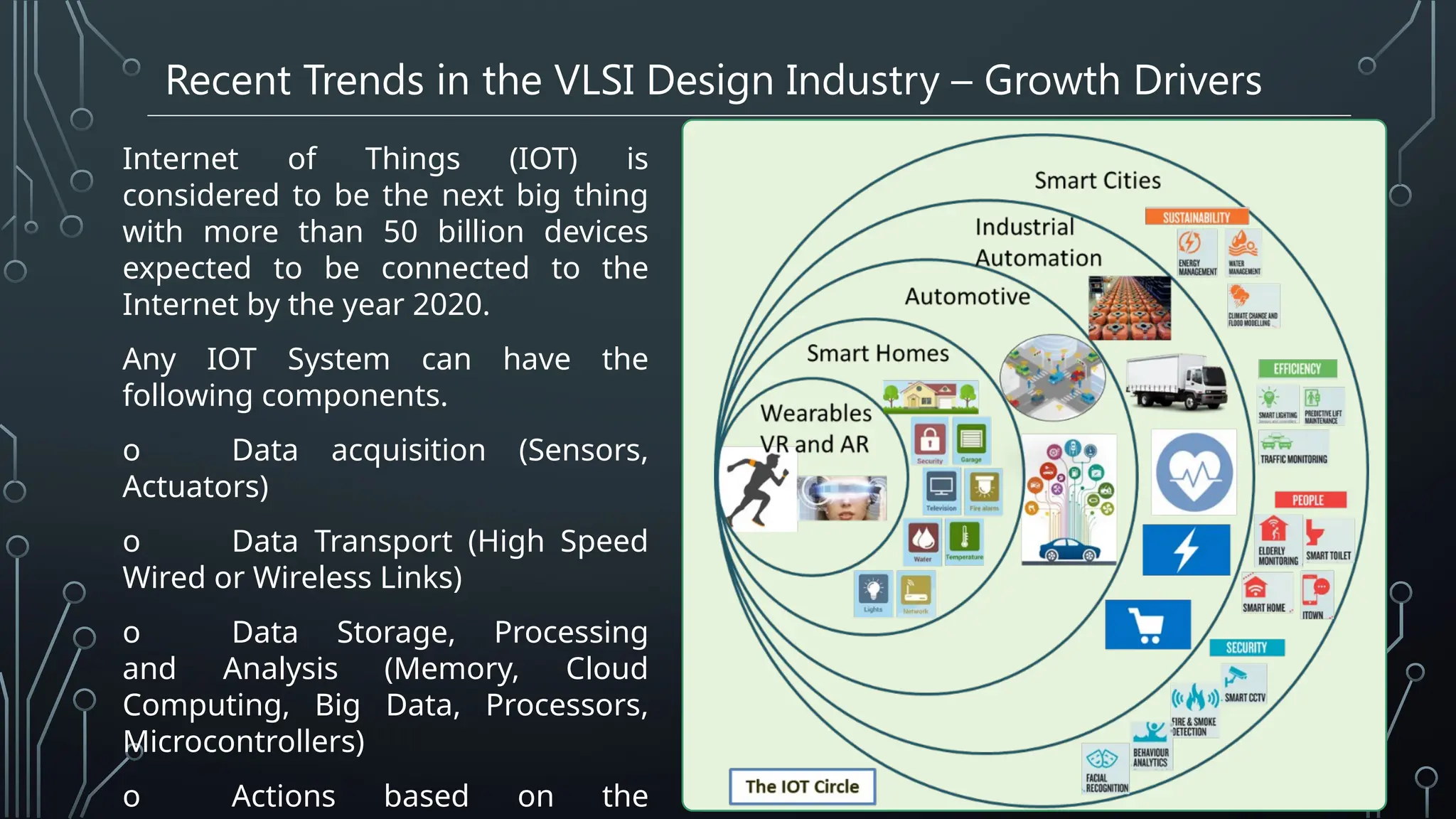
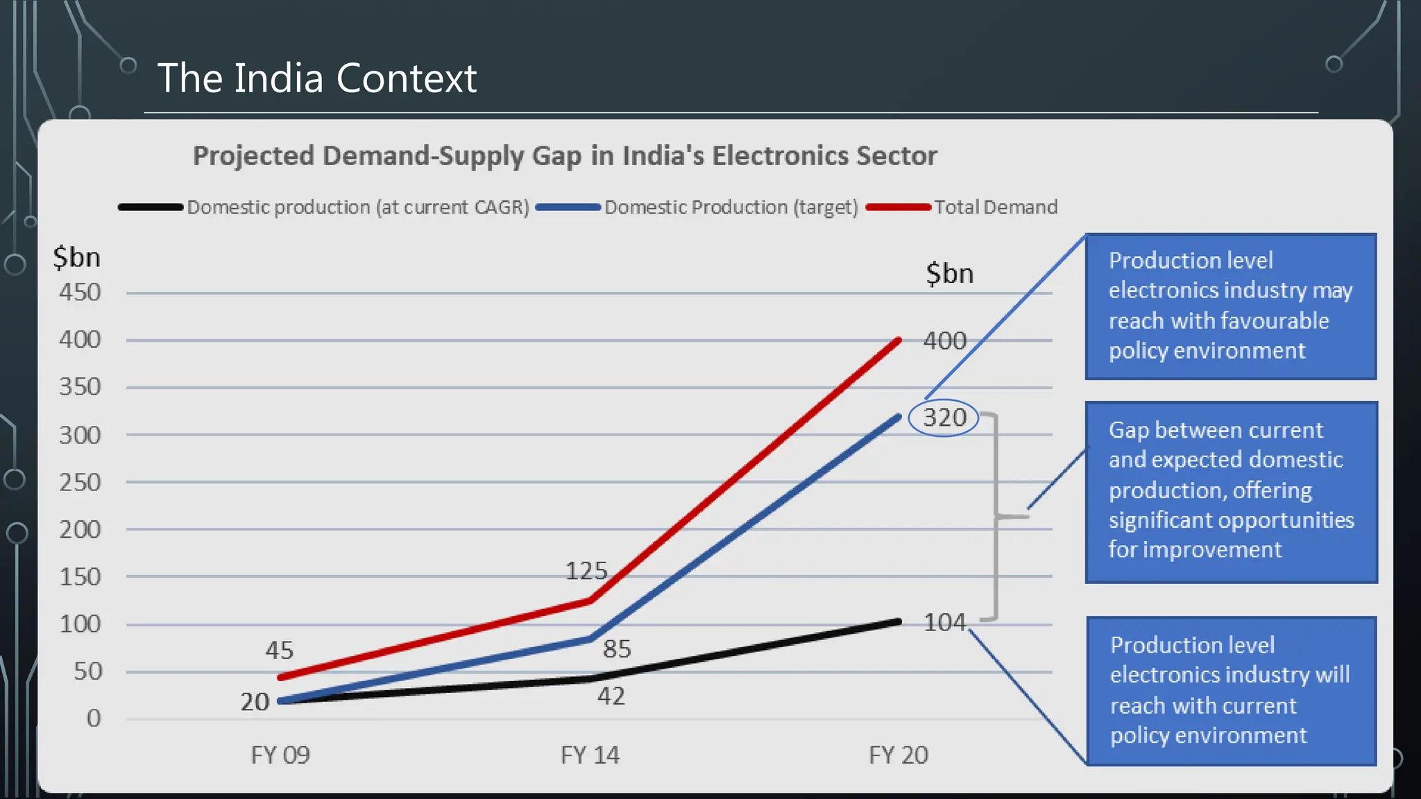
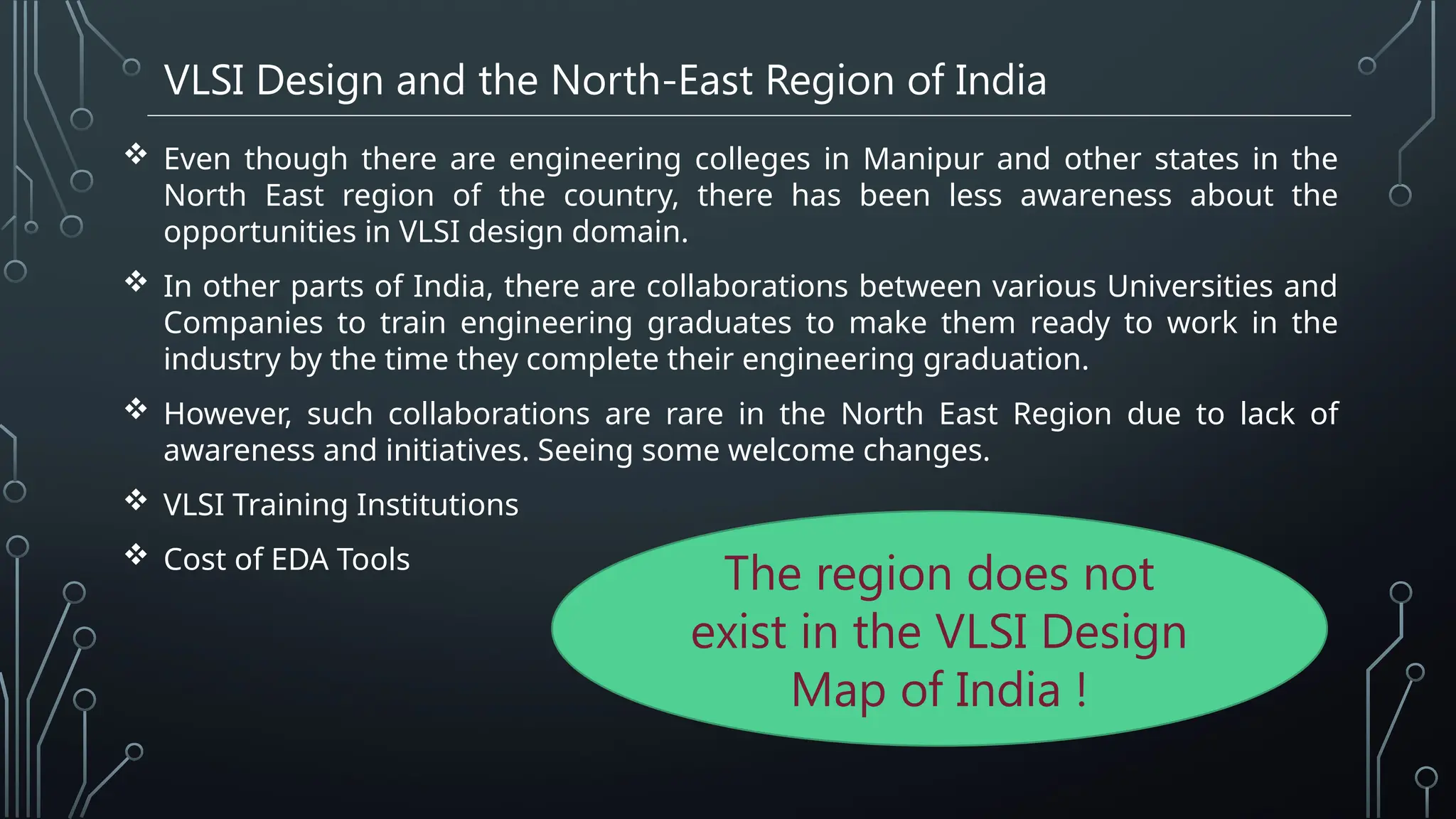
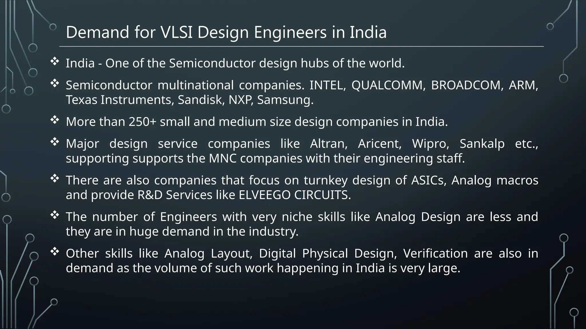
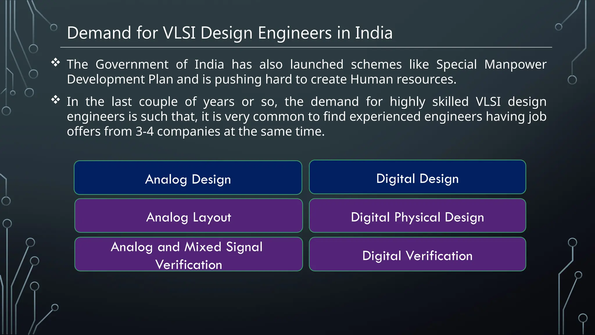
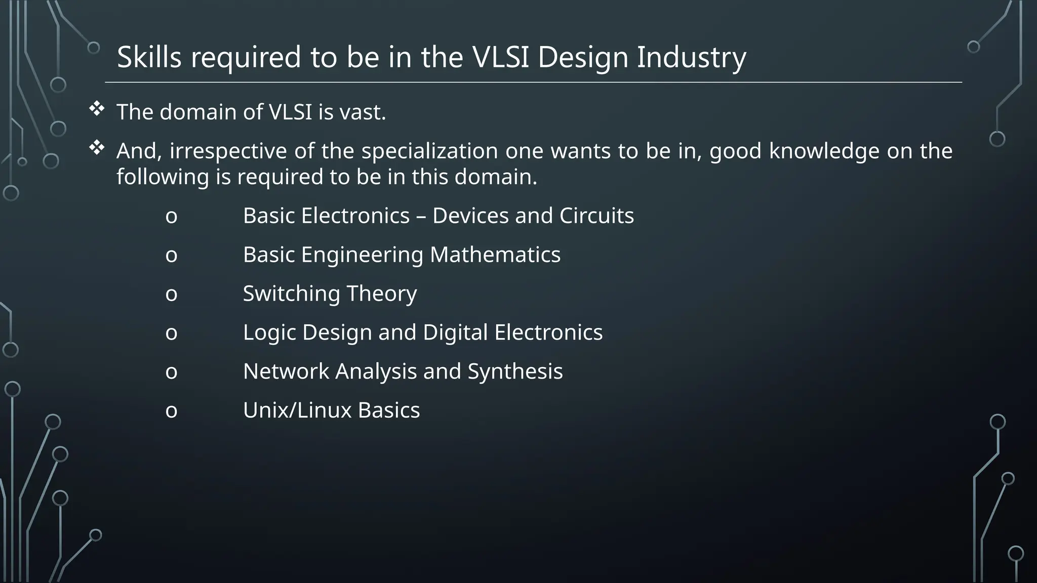
VLSI Design
An Introduction
 Founder and Managing Director of ELVEEGO Circuits Pvt. Ltd.
 ELVEEGO is a VLSI Design Company having teams in Bangalore, Tokyo and
Sapporo.
 8 years old company.
 Collaboration with companies like SONY, TOPPAN, IDTC etc., to name a few.
 ~19 years in the VLSI Design Industry
 Worked for companies like TESLA Semiconductors, RENESAS, SCL (ISRO) etc.,
 Senior Member of IEEE
(https://www.linkedin.com/in/ukningthoujam)
Uttamkumar Ningthoujam
Agenda
Introduction to VLSI Design
An Electronic System
What is VLSI Design ? Integrated Circuits.
How is VLSI Design done?
Recent Trends in the VLSI Design Industry?
VLSI Design Scenario in India.
Career in VLSI Design.
Introduction : Electronic System – Simplest Block Diagram
Input Output
Peripherals
/
Interfaces
/
Sensors
/
Transducers
Peripherals
/
Interfaces
/
Mechanical
Systems
/
Transducers
Software
Hardware
Real World System – A Smartphone Hardware
Hardware
Examples of
Motherboard
Integrated Circuits - ICs
 A set of electronic circuits on one small flat piece (or "chip") of semiconductor
material, normally silicon.
 ICs are now used in virtually all electronic equipment and have revolutionized the
world of electronics.
 Evolution
Size Cost
Performance
Speed, Power Consumption
We have come a long way from the era of Vacuum Tubes to the days of Nanotechnology.
Vacuum Tubes to Integrated Circuits – A brief history
Integrated Circuits – Classification
Small scale integration : 1965 ~ : Up to 100 devices on
a chip
Medium scale integration : till 1971 : 100-3,000 devices on
a chip
Large scale integration : 1971-1977 : 3,000-100,000
devices on a chip
Very large scale integration : 1978-2004 : 100,000 -100,000,000
devices on a chip
Ultra large scale integration : 2004 ~ : 100 million – Billions of
devices on a chip
Integrated Circuits – Package
Packages are
selected mostly
based on application
like target operating
speed, noise
condition,
temperature
conditions etc.,
Integrated Circuits – Package Bonding
Integrated Circuits – Wafer
Integrated Circuits – Wafer Dicing
Integrated Circuits – Various Types and Classification
Analog Circuits
Digital Circuits
Mixed Signal Circuits
Depending on the kind of application and circuit
type etc., Integrated Circuits can be categorised
into various types.
Making of an IC
Electronic System Requirements
Architectures and Specifications
IC Design Process
Analog Design Flow
Digital Design Flow
Mixed Signal Design Flow
IC Fabrication -> Silicon Wafer / Die
IC Testing
Design and Fabrication
EDA Tools Manufacturing Foundry
EDA Tools
Cadence
Mentor Graphics
Synopsys
Agilent
Foundry and Technologies
Manufacturing Foundries
Foundry and Technologies
Technology Nodes
G
S D
Length
Width
Feature Size
IC Design Process
Circuit
Analog
Digital
Mixed Signal
EDA Tools
Circuit Drawing
Simulator
Layout Design
Design Rule Checker
Layout V/S Schematic Checker
Parasitic Extractor
Foundry Data (PDK)
Device Symbols
Mathematical models
Layout Cells
Layout Rule Files
Parasitic Extraction Models
Analog Design Flow
Digital Design Flow
Mixed Signal Design Flow
IC Design Process – Analog Design Flow
Schematic / Circuit Design and Entry
Functional and Performance
Verification by Simulation
Layout Design
Physical Verification for LVS/DRC/ERC
Checks etc.,
Post-Layout circuit extraction with
parasitic elements.
Simulation Verification on extracted
circuit with parasitic elements.
GDS Release / Tape Out
IC Design Process – Analog Design Flow
IC Design Process – Digital Design Flow
RTL Design
Functional and Timing Verification
Synthesis
Gate Level Timing verification
Placement
Clock Tree Design
Routing
Timing Verification with Parasitic
elements
GDS Release / Tape Out
IC Design Process – Digital Design Flow
RTL Design
Functional and Timing Verification
Synthesis
Gate Level Timing verification
Placement
Clock Tree Design
Routing
Timing Verification with Parasitic
elements
GDS Release / Tape Out
IC Design Process – Digital Design Flow
Schematic, Layout and Cross Sectional View
Circuit Schematic
Top View - Layout
Cross Sectional View
Short Break
and
Design and Layout Demo
Followed By:
- Recent Trends
- Career in VLSI
Recent Trends in VLSI
Recent Trends in the VLSI Design Industry – Growth Drivers
Television
Personal Computers
Smart Phones
Internet of Things
Wearable Electronics
VR and AR
Autonomous Cars
Big Data and Cloud
Smart Cities
Recent Trends in the VLSI Design Industry – Growth Drivers
Numerous
Opportunities
and Demands
Recent Trends in the VLSI Design Industry – Growth Drivers
Internet of Things (IOT) is
considered to be the next big thing
with more than 50 billion devices
expected to be connected to the
Internet by the year 2020.
Any IOT System can have the
following components.
o Data acquisition (Sensors,
Actuators)
o Data Transport (High Speed
Wired or Wireless Links)
o Data Storage, Processing
and Analysis (Memory, Cloud
Computing, Big Data, Processors,
Microcontrollers)
o Actions based on the
The India Context
Apart from the global demand and growth prospects in Electronics, India is being
confronted with a special problem with respect to Electronics manufacturing.
The top three imports India make from other nations are
 Petroleum
 Gold
 Electronics
The India Context
The India Context
 This means, by the year 2020, electronics will surpass Oil as the largest imported
item in India, thereby creating a huge trade deficit for the country.
 To bridge this gap, the Indian Government has brought in lots of new policies to
encourage domestic electronics production, including Semiconductor design
companies, electronic device and equipment making companies.
 The Government is also working on setting up of state of the art Wafer Fabs and
many manufacturing clusters in India.
National Policy on Electronics
Skill India, SMDP
Digital India, Smart Cities
Semiconductor Policy
Make in India
VLSI Design and the North-East Region of India
 Even though there are engineering colleges in Manipur and other states in the
North East region of the country, there has been less awareness about the
opportunities in VLSI design domain.
 In other parts of India, there are collaborations between various Universities and
Companies to train engineering graduates to make them ready to work in the
industry by the time they complete their engineering graduation.
 However, such collaborations are rare in the North East Region due to lack of
awareness and initiatives. Seeing some welcome changes.
 VLSI Training Institutions
 Cost of EDA Tools
The region does not
exist in the VLSI Design
Map of India !
Demand for VLSI Design Engineers in India
 India - One of the Semiconductor design hubs of the world.
 Semiconductor multinational companies. INTEL, QUALCOMM, BROADCOM, ARM,
Texas Instruments, Sandisk, NXP, Samsung.
 More than 250+ small and medium size design companies in India.
 Major design service companies like Altran, Aricent, Wipro, Sankalp etc.,
supporting supports the MNC companies with their engineering staff.
 There are also companies that focus on turnkey design of ASICs, Analog macros
and provide R&D Services like ELVEEGO CIRCUITS.
 The number of Engineers with very niche skills like Analog Design are less and
they are in huge demand in the industry.
 Other skills like Analog Layout, Digital Physical Design, Verification are also in
demand as the volume of such work happening in India is very large.
Demand for VLSI Design Engineers in India
 The Government of India has also launched schemes like Special Manpower
Development Plan and is pushing hard to create Human resources.
 In the last couple of years or so, the demand for highly skilled VLSI design
engineers is such that, it is very common to find experienced engineers having job
offers from 3-4 companies at the same time.
Analog Design
Analog Layout
Digital Design
Digital Physical Design
Analog and Mixed Signal
Verification
Digital Verification
Skills required to be in the VLSI Design Industry
 The domain of VLSI is vast.
 And, irrespective of the specialization one wants to be in, good knowledge on the
following is required to be in this domain.
o Basic Electronics – Devices and Circuits
o Basic Engineering Mathematics
o Switching Theory
o Logic Design and Digital Electronics
o Network Analysis and Synthesis
o Unix/Linux Basics
Skills required to be in the VLSI Design Industry
 To excel in Analog Design, one need to have good command in:
o CMOS and Bipolar Device Physics, Device Operation and
Characteristics
o Circuit and Network Analysis and Synthesis
o Control Systems, Feedback and Stability Considerations and Analysis
o Electronic Devices and Circuits
o Analog Building Blocks like Opamps, Voltage and Current References,
Clock Circuits, PLLs, Data Converters etc.,
o Layout Concepts
o CMOS Technology, Device modelling and Fabrication process
o Usage of EDA Tools, Design and Verification Methodologies
Skills required to be in the VLSI Design Industry
 To excel in Digital Design, one need to have command in:
o Logic Design and Timing Analysis
o Hardware Description Language (HDL) like Verilog or VHDL
o RTL coding , Functional verification,
o Synthesis, GLS, DFT,
o Clock Specification, Power Domain Definitions and STA, Scripting
languages such as Perl,
o Usage of EDA Tools, Design and Verification Methodologies
Skills required to be in the VLSI Design Industry
 There are some areas in VLSI which are comparatively easier to enter like:
o Analog Layout
o Analog and Mixed Signal Verification
o Digital Verification
o Digital Physical Design
 There are various VLSI design training institutions in places like Bangalore,
Hyderabad, Delhi offering advanced training courses with duration of 3-6 Months.
 The best way for a fresh engineering graduate to enter VLSI design is to intern at
a design company.
 Also getting 3-6 months of training from a specialized training institution and then
attempt to enter the industry as a fresher.
Demand, Gaps and Opportunities
 Catch 22 !
High Demand
Difficulty to enter the domain
Gap in Skill
Huge Career Growth Potential
Evergreen
Domain !
Attractive
Growth !
Huge
Opportunities !
Any Questions ?
Thank You !
and
Best Wishes !
uttamkningthoujam@gmail.com

An Introduction to CMOS VLSI Design Feb10.pptx

  • 1.
  • 2.
     Founder andManaging Director of ELVEEGO Circuits Pvt. Ltd.  ELVEEGO is a VLSI Design Company having teams in Bangalore, Tokyo and Sapporo.  8 years old company.  Collaboration with companies like SONY, TOPPAN, IDTC etc., to name a few.  ~19 years in the VLSI Design Industry  Worked for companies like TESLA Semiconductors, RENESAS, SCL (ISRO) etc.,  Senior Member of IEEE (https://www.linkedin.com/in/ukningthoujam) Uttamkumar Ningthoujam
  • 3.
    Agenda Introduction to VLSIDesign An Electronic System What is VLSI Design ? Integrated Circuits. How is VLSI Design done? Recent Trends in the VLSI Design Industry? VLSI Design Scenario in India. Career in VLSI Design.
  • 4.
    Introduction : ElectronicSystem – Simplest Block Diagram Input Output Peripherals / Interfaces / Sensors / Transducers Peripherals / Interfaces / Mechanical Systems / Transducers Software Hardware
  • 5.
    Real World System– A Smartphone Hardware
  • 6.
    Real World System– A Smartphone Hardware
  • 7.
  • 8.
    Integrated Circuits -ICs  A set of electronic circuits on one small flat piece (or "chip") of semiconductor material, normally silicon.  ICs are now used in virtually all electronic equipment and have revolutionized the world of electronics.  Evolution Size Cost Performance Speed, Power Consumption
  • 9.
    We have comea long way from the era of Vacuum Tubes to the days of Nanotechnology. Vacuum Tubes to Integrated Circuits – A brief history
  • 10.
    Integrated Circuits –Classification Small scale integration : 1965 ~ : Up to 100 devices on a chip Medium scale integration : till 1971 : 100-3,000 devices on a chip Large scale integration : 1971-1977 : 3,000-100,000 devices on a chip Very large scale integration : 1978-2004 : 100,000 -100,000,000 devices on a chip Ultra large scale integration : 2004 ~ : 100 million – Billions of devices on a chip
  • 11.
    Integrated Circuits –Package Packages are selected mostly based on application like target operating speed, noise condition, temperature conditions etc.,
  • 12.
    Integrated Circuits –Package Bonding
  • 13.
  • 14.
  • 15.
    Integrated Circuits –Various Types and Classification Analog Circuits Digital Circuits Mixed Signal Circuits Depending on the kind of application and circuit type etc., Integrated Circuits can be categorised into various types.
  • 16.
    Making of anIC Electronic System Requirements Architectures and Specifications IC Design Process Analog Design Flow Digital Design Flow Mixed Signal Design Flow IC Fabrication -> Silicon Wafer / Die IC Testing
  • 17.
    Design and Fabrication EDATools Manufacturing Foundry
  • 18.
  • 19.
  • 20.
    Foundry and Technologies TechnologyNodes G S D Length Width Feature Size
  • 21.
    IC Design Process Circuit Analog Digital MixedSignal EDA Tools Circuit Drawing Simulator Layout Design Design Rule Checker Layout V/S Schematic Checker Parasitic Extractor Foundry Data (PDK) Device Symbols Mathematical models Layout Cells Layout Rule Files Parasitic Extraction Models Analog Design Flow Digital Design Flow Mixed Signal Design Flow
  • 22.
    IC Design Process– Analog Design Flow Schematic / Circuit Design and Entry Functional and Performance Verification by Simulation Layout Design Physical Verification for LVS/DRC/ERC Checks etc., Post-Layout circuit extraction with parasitic elements. Simulation Verification on extracted circuit with parasitic elements. GDS Release / Tape Out
  • 23.
    IC Design Process– Analog Design Flow
  • 24.
    IC Design Process– Analog Design Flow
  • 25.
    IC Design Process– Digital Design Flow RTL Design Functional and Timing Verification Synthesis Gate Level Timing verification Placement Clock Tree Design Routing Timing Verification with Parasitic elements GDS Release / Tape Out
  • 26.
    IC Design Process– Digital Design Flow RTL Design Functional and Timing Verification Synthesis Gate Level Timing verification Placement Clock Tree Design Routing Timing Verification with Parasitic elements GDS Release / Tape Out
  • 27.
    IC Design Process– Digital Design Flow
  • 28.
    Schematic, Layout andCross Sectional View Circuit Schematic Top View - Layout Cross Sectional View
  • 29.
    Short Break and Design andLayout Demo Followed By: - Recent Trends - Career in VLSI
  • 30.
  • 31.
    Recent Trends inthe VLSI Design Industry – Growth Drivers Television Personal Computers Smart Phones Internet of Things Wearable Electronics VR and AR Autonomous Cars Big Data and Cloud Smart Cities
  • 32.
    Recent Trends inthe VLSI Design Industry – Growth Drivers Numerous Opportunities and Demands
  • 33.
    Recent Trends inthe VLSI Design Industry – Growth Drivers Internet of Things (IOT) is considered to be the next big thing with more than 50 billion devices expected to be connected to the Internet by the year 2020. Any IOT System can have the following components. o Data acquisition (Sensors, Actuators) o Data Transport (High Speed Wired or Wireless Links) o Data Storage, Processing and Analysis (Memory, Cloud Computing, Big Data, Processors, Microcontrollers) o Actions based on the
  • 34.
    The India Context Apartfrom the global demand and growth prospects in Electronics, India is being confronted with a special problem with respect to Electronics manufacturing. The top three imports India make from other nations are  Petroleum  Gold  Electronics
  • 35.
  • 36.
    The India Context This means, by the year 2020, electronics will surpass Oil as the largest imported item in India, thereby creating a huge trade deficit for the country.  To bridge this gap, the Indian Government has brought in lots of new policies to encourage domestic electronics production, including Semiconductor design companies, electronic device and equipment making companies.  The Government is also working on setting up of state of the art Wafer Fabs and many manufacturing clusters in India. National Policy on Electronics Skill India, SMDP Digital India, Smart Cities Semiconductor Policy Make in India
  • 37.
    VLSI Design andthe North-East Region of India  Even though there are engineering colleges in Manipur and other states in the North East region of the country, there has been less awareness about the opportunities in VLSI design domain.  In other parts of India, there are collaborations between various Universities and Companies to train engineering graduates to make them ready to work in the industry by the time they complete their engineering graduation.  However, such collaborations are rare in the North East Region due to lack of awareness and initiatives. Seeing some welcome changes.  VLSI Training Institutions  Cost of EDA Tools The region does not exist in the VLSI Design Map of India !
  • 38.
    Demand for VLSIDesign Engineers in India  India - One of the Semiconductor design hubs of the world.  Semiconductor multinational companies. INTEL, QUALCOMM, BROADCOM, ARM, Texas Instruments, Sandisk, NXP, Samsung.  More than 250+ small and medium size design companies in India.  Major design service companies like Altran, Aricent, Wipro, Sankalp etc., supporting supports the MNC companies with their engineering staff.  There are also companies that focus on turnkey design of ASICs, Analog macros and provide R&D Services like ELVEEGO CIRCUITS.  The number of Engineers with very niche skills like Analog Design are less and they are in huge demand in the industry.  Other skills like Analog Layout, Digital Physical Design, Verification are also in demand as the volume of such work happening in India is very large.
  • 39.
    Demand for VLSIDesign Engineers in India  The Government of India has also launched schemes like Special Manpower Development Plan and is pushing hard to create Human resources.  In the last couple of years or so, the demand for highly skilled VLSI design engineers is such that, it is very common to find experienced engineers having job offers from 3-4 companies at the same time. Analog Design Analog Layout Digital Design Digital Physical Design Analog and Mixed Signal Verification Digital Verification
  • 40.
    Skills required tobe in the VLSI Design Industry  The domain of VLSI is vast.  And, irrespective of the specialization one wants to be in, good knowledge on the following is required to be in this domain. o Basic Electronics – Devices and Circuits o Basic Engineering Mathematics o Switching Theory o Logic Design and Digital Electronics o Network Analysis and Synthesis o Unix/Linux Basics
  • 41.
    Skills required tobe in the VLSI Design Industry  To excel in Analog Design, one need to have good command in: o CMOS and Bipolar Device Physics, Device Operation and Characteristics o Circuit and Network Analysis and Synthesis o Control Systems, Feedback and Stability Considerations and Analysis o Electronic Devices and Circuits o Analog Building Blocks like Opamps, Voltage and Current References, Clock Circuits, PLLs, Data Converters etc., o Layout Concepts o CMOS Technology, Device modelling and Fabrication process o Usage of EDA Tools, Design and Verification Methodologies
  • 42.
    Skills required tobe in the VLSI Design Industry  To excel in Digital Design, one need to have command in: o Logic Design and Timing Analysis o Hardware Description Language (HDL) like Verilog or VHDL o RTL coding , Functional verification, o Synthesis, GLS, DFT, o Clock Specification, Power Domain Definitions and STA, Scripting languages such as Perl, o Usage of EDA Tools, Design and Verification Methodologies
  • 43.
    Skills required tobe in the VLSI Design Industry  There are some areas in VLSI which are comparatively easier to enter like: o Analog Layout o Analog and Mixed Signal Verification o Digital Verification o Digital Physical Design  There are various VLSI design training institutions in places like Bangalore, Hyderabad, Delhi offering advanced training courses with duration of 3-6 Months.  The best way for a fresh engineering graduate to enter VLSI design is to intern at a design company.  Also getting 3-6 months of training from a specialized training institution and then attempt to enter the industry as a fresher.
  • 44.
    Demand, Gaps andOpportunities  Catch 22 ! High Demand Difficulty to enter the domain Gap in Skill Huge Career Growth Potential Evergreen Domain ! Attractive Growth ! Huge Opportunities !
  • 45.
  • 46.
    Thank You ! and BestWishes ! uttamkningthoujam@gmail.com

Editor's Notes

  • #36 Healthcare: Medical Records, Medical Instruments, Smart Grids, Renewable Energy Sources Education: Online Training, Internet of Things Wearables: Fitness Bands, Jackets, Real Time Monitoring VR, AR: Holograms, Headsets Smart Homes: Surveillance, Automated Home, Power Saving, Security