The document outlines an examination for a VLSI design lab course. It contains 24 questions to be completed in 3 hours. For each question, students are instructed to either simulate a digital circuit using Xilinx ISE 9.1i software or implement the circuit using an XC3S400 FPGA trainer kit. The circuits include adders, encoders, decoders, multipliers, flip-flops, and basic logic gates.
PAM4 Analysis and Measurement Webinar Slidedeckteledynelecroy
In this Teledyne LeCroy webinar we explore the acquisition and analysis of PAM4 waveforms. We will cover PAM4 test configurations, compliance measurements and debug techniques.
PAM4 Analysis and Measurement Webinar Slidedeckteledynelecroy
In this Teledyne LeCroy webinar we explore the acquisition and analysis of PAM4 waveforms. We will cover PAM4 test configurations, compliance measurements and debug techniques.
(Video and more at fsharpforfunandprofit.com/csharp)
Curious about F# and want to understand how is it different from C#?
In this talk, we'll look at the basics of coding in F#, and how functional programming differs from object-oriented programming. Along the way, there will be many examples showing the same code written in C# and F# so that you can see for yourself how the two languages differ in style and approach.
How to create SystemVerilog verification environment?Sameh El-Ashry
Basic knowledge for the verification engineer to learn the art of creating SystemVerilog verification environment.
Starting from the specifications extraction till coverage closure.
Designed a differential input and single ended output high gain (>= 85 dB) operational amplifier using CMOS 0.35um technology using a single independent current source. The amplifier was also designed to achieve a CMRR (>= 80dB), Average Slew Rate (>= 15 V/us), UGF (>= 15 MHz) & Output Voltage Swing ( >= 1.4V). The maximum power dissipation through the complete circuit including the current source branch was limited to 0.3 mW.
Design and Verification of 4 X 4 Wallace Tree MultiplierMohd Esa
The aim of this paper is to study 4x4 Wallace tree multiplier. In high
performance processing units & computing systems, multiplication of two
binary numbers is primitive and most frequently used arithmetic operation.
Wallace tree multiplier is area efficient & high speed multiplier. This paper
presents design and verification of Wallace tree multiplier. Design is carried out
in Xilinx ISE Design Suite 14.7 using Verilog HDL and verification is carried
out in Questa Sim 10.4e using System Verilog HVL environment.
A typical design flow follows the below structure and can be broken down into multiple steps. Some of these phases happen in parallel and some in sequentially.
Requirements
A customer of a semiconductor firm is typically some other company who plans to use the chip in its systems or end products. So, the customer's requirements also play an important role in deciding how the chip should be designed.
The first step is to collect the requirements, estimate the end product's market value, and evaluate the number of resources required to do the project.
Specifications
The next step is to collect specifications that describe the functionality, interface abstractly, and over all architecture of the chip to be designed. This can be something along the lines such as:
Play
Next
Unmute
Current TimeÂ
0:00
/
DurationÂ
18:10
Â
Fullscreen
Backward Skip 10s
Play Video
Forward Skip 10s
Requires computational power to run imaging algorithms to support virtual reality.
Requires two ARM A53 processors with coherent interconnect and should run at 600 MHz.
Requires USB 3.0, Bluetooth, and PCIe 2nd gen interfaces.
It should support 1920x1080 pixel displays with an appropriate controller.
Digital Design
Because of the complex nature of modern chips, it's impossible to build something from scratch, and in many cases, many components will be reused.
For example, company A requires a FlexCAN module to interact with other modules in an automobile. They can either buy the FlexCAN design from another company to save time and effort or spend resources to build one.
It's not practical to design such a system from basic building blocks such as flip-flops and CMOS transistors.
Instead, a behavioral description is developed to analyze the design in terms of functionality, performance, and other high-level issues using a Hardware Description Language such as Verilog or VHDL.
This is usually done by a digital designer and is similar to a high-level computer programmer equipped with digital electronics skills.
Verification
Once the RTL design is ready, it needs to be verified for functional correctness.
For example, a DSP processor is expected to issue bus transactions with fetching instructions from memory and know that this will happen as expected.
The functional verification is required at this point, which is done with EDA simulators' help that can model the design and apply a different stimulus to it. This is the job of a pre-silicon verification engineer.
Logic Synthesis
Now we will convert this design into hardware schematic with real elements such as combinational gates and flip-flops. This step is called synthesis.
Logic synthesis tools enable the conversion of RTL description in HDL to a gate-level netlist. This netlist is a description of the circuit in terms of gates and connections between them.
Logic synthesis tools ensure that the netlist meets timing, area, and power specifications. Typically, they have access to different technology node
FortranCon2020: Highly Parallel Fortran and OpenACC DirectivesJeff Larkin
Fortran has long been the language of computational math and science and it has outlived many of the computer architectures on which it has been used. Modern Fortran must be able to run on modern, highly parallel, heterogeneous computer architectures. A significant number of Fortran programmers have had success programming for heterogeneous machines by pairing Fortran with the OpenACC language for directives-based parallel programming. This includes some of the most widely-used Fortran applications in the world, such as VASP and Gaussian. This presentation will discuss what makes OpenACC a good fit for Fortran programmers and what the OpenACC language is doing to promote the use of native language parallelism in Fortran, such as do concurrent and Co-arrays.
Video Recording: https://www.youtube.com/watch?v=OXZ_Wkae63Y
« Le « Machine Learning » – « Apprentissage statistique » ou « Analyse prédictive » - sort des labos de recherche et des cercles de spécialistes pour être de plus en plus être utilisé au sein des entreprises, et pas seulement les startups. En témoigne l’essor de la toolkit OpenSource Scikit-learn très vite répandue internationalement comme l’un des nouveaux standards de cette nouvelle façon de faire du logiciel, mais aussi la disponibilité depuis juillet 2014 d’Azure ML, le service de Machine Learning de Microsoft Azure. Dans cette session nous vous proposons un aperçu du développement de logiciel d’apprentissage statistique en Python avec SciKit-Learn. Nous invitons l'un des principaux contributeurs de cette toolkit, Olivier Grisel , ingénieur de recherche dans l’équipe équipe Inria PARIETAL à Saclay, à venir nous en présenter un aperçu dans une session interactive et basée sur de nombreux exemples et démos. Pour en savoir plus: http://scikit-learn.org https://team.inria.fr/parietal/ https://twitter.com/ogrisel
Penn
State
University
School
of
Electrical
Engineering
and
Computer
Science
Page
1
of
4
CMPEN
331
–
Computer
Organization
and
Design,
Lab
6
Due
Wednesday
April
26,
2017
at
7:00
am
(Drop
box
on
Canvas)
This lab introduces the idea of the pipelining technique for building a fast CPU. The students will obtain
experience with the design implementation and testing of the first four stages (Instruction Fetch, Instruction
Decode, Instruction Execute, Memory) of the five-stage pipelined CPU using the Xilinx design package for
FPGAs. It is assumed that students are familiar with the operation of the Xilinx design package for Field
Programmable Gate Arrays (FPGAs) through the Xilinix tutorial available in the class website.
1. Pipelining
As described in lab 4
2. Circuits of the Instruction Fetch Stage
As described in lab 4
3. Circuits of the Instruction Decode Stage
As described in lab 4
4. Circuits of the Execution Stage
As described in lab 5
5. Circuits of the Memory Access Stage
As described in lab 5
6. Circuits of the Write Back Stage
Referring to Figure 1, in the fifth cycle the first instruction entered the WB stage. The memory data is selected
and will be written into the register file at the end of the cycle. All the control signal have a prefix “w”. The
second instruction entered the MEM stage; the third instruction entered the EXE stage; the fourth instruction is
being decoded in the ID stage; and the fifth instruction is being fetched in the IF stage. All the six pipeline
registers are updated at the end of the cycle (the destination register is considered as the six pipeline register).
Then the first instruction is committed. In each of the forth coming clock cycles, an instruction will be commited
and a new instruction will enter the pipeline. We use the structure shown in Figure 1 as a baseline for the design
of our pipelined CPU.
Penn
State
University
School
of
Electrical
Engineering
and
Computer
Science
Page
2
of
4
Figure 1 Pipeline write back (WB) stage
7. Table 1 lists the names and usages of the 32 registers in the register file.
Table 1 MIPS general purpose register
$zero 0 Constant 0
$at 1 Reserved for assembler
$v0, $v1 2, 3 Function return values
$a0 - $a3 4 – 7 Function argument values
$t0 - $t7 8 – 15 Temporary (caller saved)
$s0 - $s7 16 – 23 Temporary (callee saved)
$t8, $t9 24, 25 Temporary (caller saved)
$k0, $k1 26, 27 Reserved for OS Kernel
$gp 28 Pointer to Global Area
$sp 29 Stack Pointer
$fp 30 Frame Pointer
$ra 31 Return Address
8. Table 2 lists some MIPS i.
Integrating microservices with apache camel on kubernetesClaus Ibsen
Apache Camel has fundamentally changed the way Java developers build system-to-system integrations by using enterprise integration patterns (EIP) with modern microservice architectures. In this session, we’ll show you best practices with Camel and EIPs, in the world of Spring Boot microservices running on Kubernetes. We'll also discuss practices how to build truly cloud-native distributed and fault-tolerant microservices and we’ll introduce the upcoming Camel 3.0 release, which includes serverless capabilities via Camel K. This talk is a mix with slides and live demos.
Similar to VLSI Anna University Practical Examination (12)
Model Attribute Check Company Auto PropertyCeline George
In Odoo, the multi-company feature allows you to manage multiple companies within a single Odoo database instance. Each company can have its own configurations while still sharing common resources such as products, customers, and suppliers.
Synthetic Fiber Construction in lab .pptxPavel ( NSTU)
Synthetic fiber production is a fascinating and complex field that blends chemistry, engineering, and environmental science. By understanding these aspects, students can gain a comprehensive view of synthetic fiber production, its impact on society and the environment, and the potential for future innovations. Synthetic fibers play a crucial role in modern society, impacting various aspects of daily life, industry, and the environment. ynthetic fibers are integral to modern life, offering a range of benefits from cost-effectiveness and versatility to innovative applications and performance characteristics. While they pose environmental challenges, ongoing research and development aim to create more sustainable and eco-friendly alternatives. Understanding the importance of synthetic fibers helps in appreciating their role in the economy, industry, and daily life, while also emphasizing the need for sustainable practices and innovation.
Unit 8 - Information and Communication Technology (Paper I).pdfThiyagu K
This slides describes the basic concepts of ICT, basics of Email, Emerging Technology and Digital Initiatives in Education. This presentations aligns with the UGC Paper I syllabus.
2024.06.01 Introducing a competency framework for languag learning materials ...Sandy Millin
http://sandymillin.wordpress.com/iateflwebinar2024
Published classroom materials form the basis of syllabuses, drive teacher professional development, and have a potentially huge influence on learners, teachers and education systems. All teachers also create their own materials, whether a few sentences on a blackboard, a highly-structured fully-realised online course, or anything in between. Despite this, the knowledge and skills needed to create effective language learning materials are rarely part of teacher training, and are mostly learnt by trial and error.
Knowledge and skills frameworks, generally called competency frameworks, for ELT teachers, trainers and managers have existed for a few years now. However, until I created one for my MA dissertation, there wasn’t one drawing together what we need to know and do to be able to effectively produce language learning materials.
This webinar will introduce you to my framework, highlighting the key competencies I identified from my research. It will also show how anybody involved in language teaching (any language, not just English!), teacher training, managing schools or developing language learning materials can benefit from using the framework.
Operation “Blue Star” is the only event in the history of Independent India where the state went into war with its own people. Even after about 40 years it is not clear if it was culmination of states anger over people of the region, a political game of power or start of dictatorial chapter in the democratic setup.
The people of Punjab felt alienated from main stream due to denial of their just demands during a long democratic struggle since independence. As it happen all over the word, it led to militant struggle with great loss of lives of military, police and civilian personnel. Killing of Indira Gandhi and massacre of innocent Sikhs in Delhi and other India cities was also associated with this movement.
CLASS 11 CBSE B.St Project AIDS TO TRADE - INSURANCE
VLSI Anna University Practical Examination
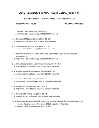
1. ANNA UNIVERSITY PRACTICAL EXAMINATION, APRIL 2011
SUB. CODE: EC2357 QUESTION PAPER SUB: VLSI DESIGN LAB
TIME DURATION: 3 HOURS MAXIMUM MARKS: 100
1. a. Simulate a serial adder using Xilinx ISE 9.1i
b. Implement a 8:3 encoder using XC3S400 FPGA trainer kit.
2. a. Simulate a PRBS generator using Xilinx ISE 9.1i
b. Implement a half adder using XC3S400 FPGA trainer kit.
3. a. Simulate an accumulator using Xilinx ISE 9.1i
b. Implement a full adder using XC3S400 FPGA trainer kit.
4. a. Draw the schematics of a CMOS NAND gate . Generate the layout automatically and
and simulate it.
b. Implement a 3:8 decoder using XC3S400 FPGA trainer kit.
5. .a. Simulate a synchronous updown counter using Xilinx ISE 9.1i
b. Implement a 4 bit multiplier using XC3S400 FPGA trainer kit.
6. a. Simulate a universal shift register using Xilinx ISE 9.1i
b. Implement a half subtractor using XC3S400 FPGA trainer kit.
7. a. Simulate a 8 bit adder using Xilinx ISE 9.1i
b. Implement a 1:8 demultiplexer using XC3S400 FPGA trainer kit.
8. a. Simulate a JK flip-flop using Xilinx ISE 9.1i
b. Implement a full subtractor using XC3S400 FPGA trainer kit
9. a. Simulate a SR flip-flop using Xilinx ISE 9.1i
b. Implement a 4:1 multiplexer using XC3S400 FPGA trainer kit
10. a. Generate the layout of a CMOS inverter and simulate .Measure the dissipated power. Find
also the dissipated power after adding 0.01 pf capacitor at the output.
b. Simulate a 8 bit multiplier using Xilinx ISE 9.1i
2. 11. a. Draw the schematics of the function F= AB + C (A+B) and simulate it.. Generate the SPICE
file.
b. Simulate a T flip flop using Xilinx ISE 9.1i
12. a . Draw the schematics of the function F= (AB + C)D . Generate the layout automatically and
and simulate it.
b. Simulate a D flip flop using Xilinx ISE 9.1i
13. a. Simulate a serial adder using Xilinx ISE 9.1i
b. Implement a 4 bit multiplier using XC3S400 FPGA trainer kit.
14 a. Simulate a PRBS generator using Xilinx ISE 9.1
b. Implement a half subtractor using XC3S400 FPGA trainer kit.
15. a. Simulate an accumulator using Xilinx ISE 9.1i
b. Implement a full subtractor using XC3S400 FPGA trainer kit.
16 a. Draw the schematics of a CMOS NOR gate . Generate the layout automatically and
and simulate it.
b. Implement a 1:8 demultiplexer using XC3S400 FPGA trainer kit.
17. a. Simulate a synchronous updown counter using Xilinx ISE 9.1i
b. Implement a 4:1 multiplexer using XC3S400 FPGA trainer kit.
18. a. Simulate a universal shift register using Xilinx ISE 9.1i
b. Implement a half adder using XC3S400 FPGA trainer kit.
19 a. Simulate a 8 bit adder using Xilinx ISE 9.1i
b. Implement a 8:3 encoder using XC3S400 FPGA trainer kit.
20. a. Simulate a JK flip-flop using Xilinx ISE 9.1i
b. Implement a full adder using XC3S400 FPGA trainer kit.
3. 21. a. Simulate a SR flip-flop using Xilinx ISE 9.1i
b. Implement a 3:8 decoder using XC3S400 FPGA trainer kit.
22. a. Generate the layout of a CMOS inverter and simulate .Measure the dissipated power. Find
also the dissipated power after adding 0.1 pf capacitor at the output.
b. Simulate a 6 bit multiplier using Xilinx ISE 9.1i
23. a. Draw the schematics of the function F= AB +B C +AC and simulate it.. Generate the
Spice file.
b. Simulate a T flip flop using Xilinx ISE 9.1i
24. a. Draw the schematics of the function F= AB C +D . Generate the layout automatically and
and simulate it.
b. Simulate a D flip flop using Xilinx ISE 9.1i