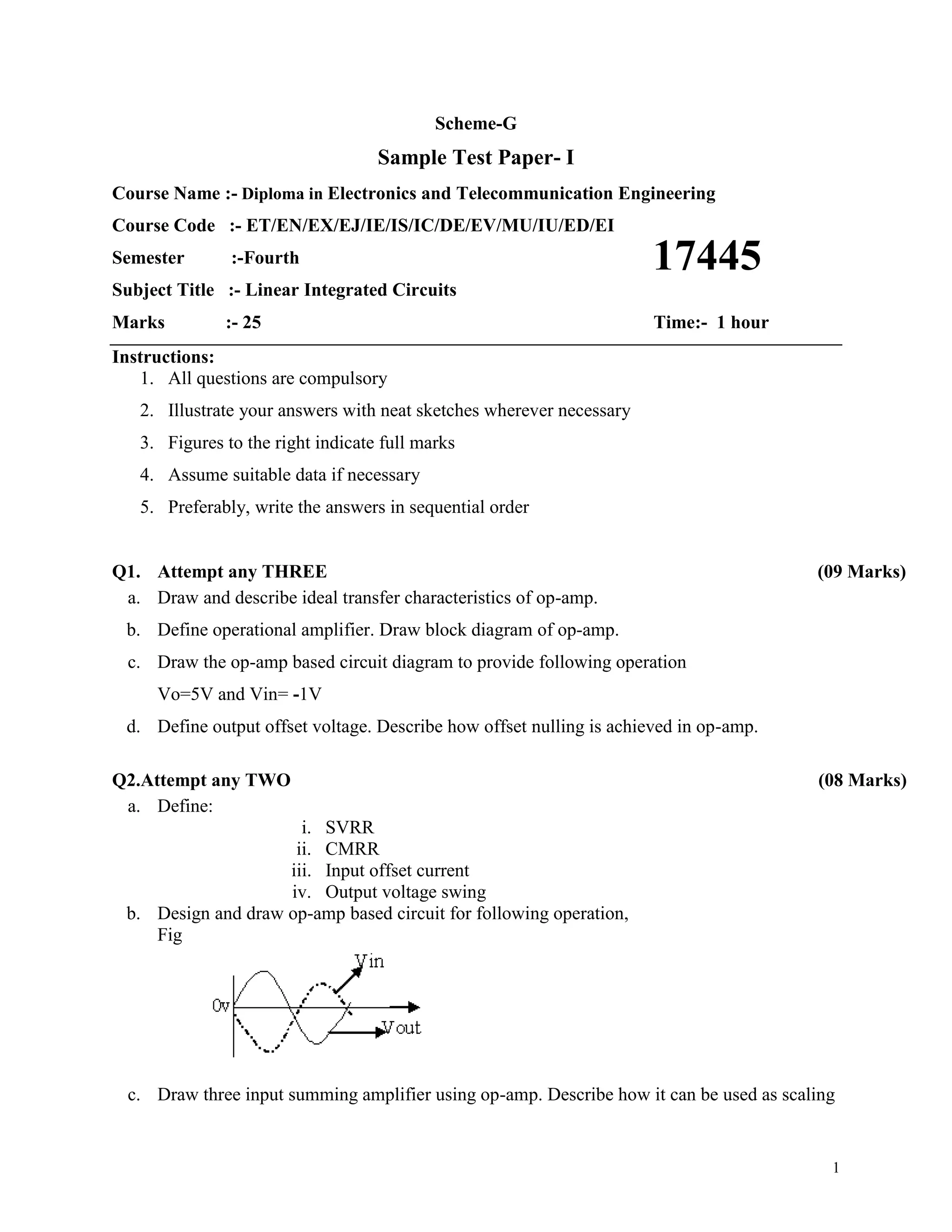
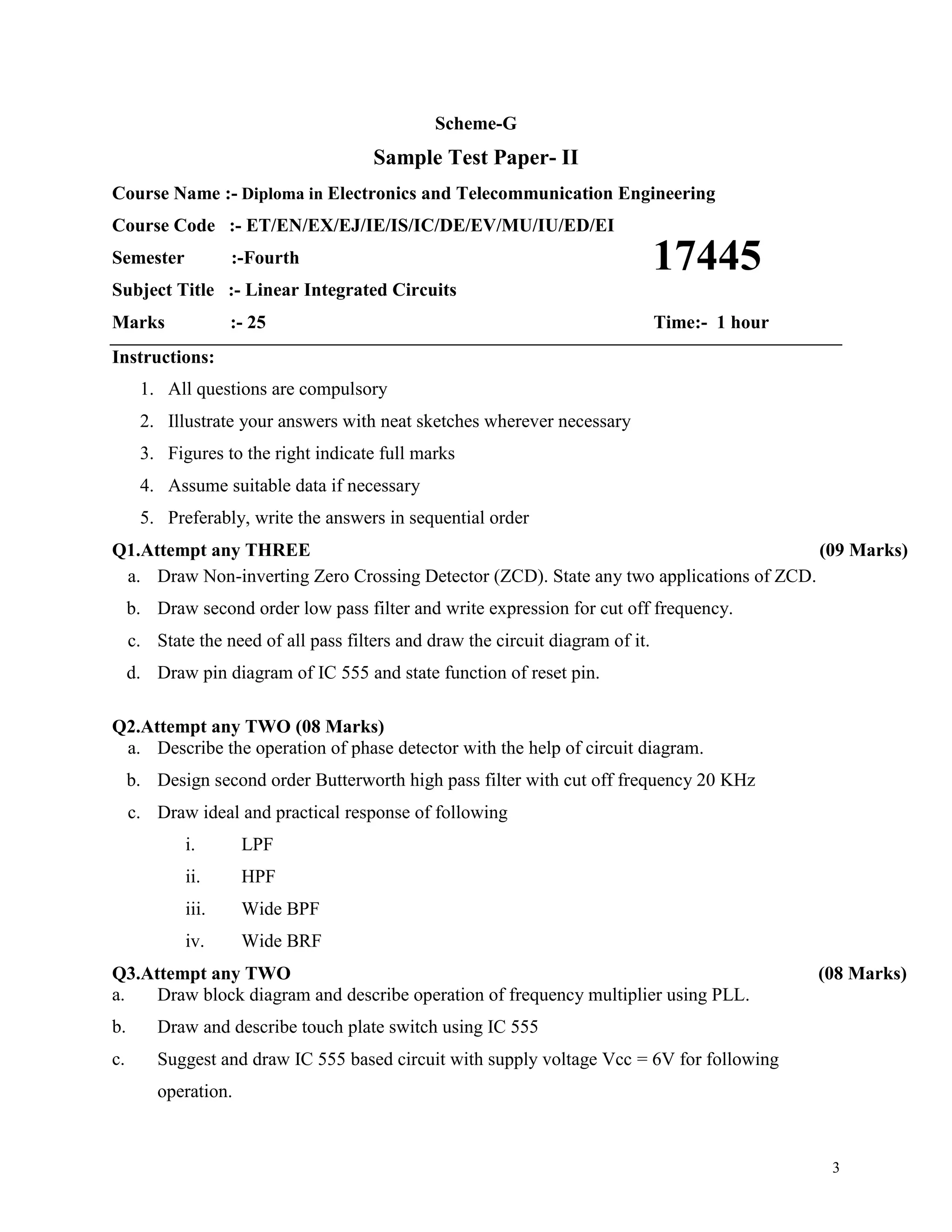
This document contains 6 sample question papers for an exam on Linear Integrated Circuits. Each paper contains 3-6 questions with multiple parts assessing various concepts related to operational amplifiers, filters, instrumentation amplifiers, timers and oscillators using op-amps and IC 555. The questions include topics like ideal op-amp characteristics, filter design and analysis, signal conditioning circuits, timer applications and phase locked loops. Students are required to draw circuits, derive expressions and describe concepts with diagrams to solve the problems.
At low frequencies, we analyze transistor
using h-parameter. But for high frequency analysis the
h-parameter model is not suitable, because :-
(1) The value of h-parameters are not constant at high frequencies.
(2)At high frequency h-parameters becomes very complex
in nature
Hybrid pi model of a Transistor. And designing of pi model using transistor with internal capacitances & internal resistance default considerations. along with CE short channel current gain with and without load. and also FET analysis its equivalent circuits.in FET analysis we have common source and common drain type of systems along with their equivalent circuits and analysis. capture these images and findout the solution for your hybid pi model high frequncy nature of a transistor. All the best. keep in contact with my linkedin.
Conventional power amplifier systems trade-off efficiency for linearity due to transistor operation limitations. The Smart Power Amplifier architecture improves RF Power Amplifier linearity without compromising efficiency. This novel invention generates and utilizes specialized outphased signals that can be used in outphasing RF power amplifiers in order to amplify the input signal without suffering from the nonlinearities and inefficiencies associated with conventional power amplifiers. Using this proposed technique, designers and developers can generate variable number of outphased signals on the fly with minimal processing and memory footprints. The proposed architecture for constructing and combining a variable number of constant amplitude outphased signals results in both highly linear and significantly efficient power amplification system. The complexities of both constructing and combining the decomposed signals are significantly reduced due to the fact that all of the decomposed signals except only two of them are actually scaled versions of the input signal.
In this paper Low power low voltage CMOS analog multiplier circuit is proposed. It is based on flipped voltage
follower. It consists of four voltage adders and a multiplier core. The circuit is analyzed and designed in 0.18um
CMOS process model and simulation results have shown that, under single 0.9V supply voltage, and it
consumes only 31.8μW quiescent power and 110MHZ bandwidth.
DIFFERENTIAL AMPLIFIER using MOSFET, Modes of operation,
The MOS differential pair with a common-mode input voltage ,Common mode rejection,gain, advantages and disadvantages.
This Presentation is related to multistage amplifiers. different topics related to multistage amplifiers like two stage amplifiers. Two stage RC coupled amplifiers, cascading techniques, CE-CB cascod amplifiers, darlington pair, fet analysis
UN PEQUEÑO RESUMEN DE LO QUE DOS DE LOS 4 TEJIDOS MAS IMPORTANTES EN NUESTRO CUERPO HACEN POR NOSOTROS ADEMAS DE TENER UN APORTE Y UNA PEQUEÑA MUESTRA DE MAPAS PARA ACLARAR LA PARTICIPACIÓN DE EL TEJIDO NERVIOSO Y EL TEJIDO MUSCULAR.
ESTA PRESENTACIÓN ES CON EL FIN DE DESCRIBIR DESDE LA DEFINICIÓN DEL TEJIDO,CONTINUANDO CON SUS CARACTERÍSTICA Y SUS FUNCIONES EN EL CUERPO HUMANO QUE NOS PERMITE MOVERNOS .
This is the image sensing technology base pwerpoint presentation which highlights the basics of image sensing...
Image sensing is a technology of recognising a image or comparing a image or taking a image...
nicely view , types of computer know information and lots of picture in computers and parts of fields.
here three category divide to know computer struture .
Electrical current, voltage, resistance, capacitance, and inductance are a few of the basic elements of electronics and radio. Apart from current, voltage, resistance, capacitance, and inductance, there are many other interesting elements to electronic technology. ... Use Electronics Notes to learn electronics online.
Unit 8 - Information and Communication Technology (Paper I).pdfThiyagu K
This slides describes the basic concepts of ICT, basics of Email, Emerging Technology and Digital Initiatives in Education. This presentations aligns with the UGC Paper I syllabus.
Macroeconomics- Movie Location
This will be used as part of your Personal Professional Portfolio once graded.
Objective:
Prepare a presentation or a paper using research, basic comparative analysis, data organization and application of economic information. You will make an informed assessment of an economic climate outside of the United States to accomplish an entertainment industry objective.
The French Revolution, which began in 1789, was a period of radical social and political upheaval in France. It marked the decline of absolute monarchies, the rise of secular and democratic republics, and the eventual rise of Napoleon Bonaparte. This revolutionary period is crucial in understanding the transition from feudalism to modernity in Europe.
For more information, visit-www.vavaclasses.com
Palestine last event orientationfvgnh .pptxRaedMohamed3
An EFL lesson about the current events in Palestine. It is intended to be for intermediate students who wish to increase their listening skills through a short lesson in power point.
Introduction to AI for Nonprofits with Tapp NetworkTechSoup
Dive into the world of AI! Experts Jon Hill and Tareq Monaur will guide you through AI's role in enhancing nonprofit websites and basic marketing strategies, making it easy to understand and apply.
Instructions for Submissions thorugh G- Classroom.pptxJheel Barad
This presentation provides a briefing on how to upload submissions and documents in Google Classroom. It was prepared as part of an orientation for new Sainik School in-service teacher trainees. As a training officer, my goal is to ensure that you are comfortable and proficient with this essential tool for managing assignments and fostering student engagement.
Acetabularia Information For Class 9 .docxvaibhavrinwa19
Acetabularia acetabulum is a single-celled green alga that in its vegetative state is morphologically differentiated into a basal rhizoid and an axially elongated stalk, which bears whorls of branching hairs. The single diploid nucleus resides in the rhizoid.
Read| The latest issue of The Challenger is here! We are thrilled to announce that our school paper has qualified for the NATIONAL SCHOOLS PRESS CONFERENCE (NSPC) 2024. Thank you for your unwavering support and trust. Dive into the stories that made us stand out!
1. 1
Scheme-G
Sample Test Paper- I
Course Name :- Diploma in Electronics and Telecommunication Engineering
Course Code :- ET/EN/EX/EJ/IE/IS/IC/DE/EV/MU/IU/ED/EI
Semester :-Fourth
Subject Title :- Linear Integrated Circuits
Marks :- 25 Time:- 1 hour
Instructions:
1. All questions are compulsory
2. Illustrate your answers with neat sketches wherever necessary
3. Figures to the right indicate full marks
4. Assume suitable data if necessary
5. Preferably, write the answers in sequential order
Q1. Attempt any THREE (09 Marks)
a. Draw and describe ideal transfer characteristics of op-amp.
b. Define operational amplifier. Draw block diagram of op-amp.
c. Draw the op-amp based circuit diagram to provide following operation
Vo=5V and Vin= -1V
d. Define output offset voltage. Describe how offset nulling is achieved in op-amp.
Q2.Attempt any TWO (08 Marks)
a. Define:
i. SVRR
ii. CMRR
iii. Input offset current
iv. Output voltage swing
b. Design and draw op-amp based circuit for following operation,
Fig
c. Draw three input summing amplifier using op-amp. Describe how it can be used as scaling
17445
2. 2
amplifier.
Q3.Attempt any TWO (08 Marks)
a. Draw op-amp based circuit for following operation
Vo = -(V1+V2+V3)/3
Also state the value of input resistor if Rf=3KΩ
b. List any four advantages of instrumentation amplifier
c. Draw and describe I to V converter using op-amp
3. 3
Scheme-G
Sample Test Paper- II
Course Name :- Diploma in Electronics and Telecommunication Engineering
Course Code :- ET/EN/EX/EJ/IE/IS/IC/DE/EV/MU/IU/ED/EI
Semester :-Fourth
Subject Title :- Linear Integrated Circuits
Marks :- 25 Time:- 1 hour
Instructions:
1. All questions are compulsory
2. Illustrate your answers with neat sketches wherever necessary
3. Figures to the right indicate full marks
4. Assume suitable data if necessary
5. Preferably, write the answers in sequential order
Q1.Attempt any THREE (09 Marks)
a. Draw Non-inverting Zero Crossing Detector (ZCD). State any two applications of ZCD.
b. Draw second order low pass filter and write expression for cut off frequency.
c. State the need of all pass filters and draw the circuit diagram of it.
d. Draw pin diagram of IC 555 and state function of reset pin.
Q2.Attempt any TWO (08 Marks)
a. Describe the operation of phase detector with the help of circuit diagram.
b. Design second order Butterworth high pass filter with cut off frequency 20 KHz
c. Draw ideal and practical response of following
i. LPF
ii. HPF
iii. Wide BPF
iv. Wide BRF
Q3.Attempt any TWO (08 Marks)
a. Draw block diagram and describe operation of frequency multiplier using PLL.
b. Draw and describe touch plate switch using IC 555
c. Suggest and draw IC 555 based circuit with supply voltage Vcc = 6V for following
operation.
17445
5. 5
Scheme-G
Sample Question Paper
Course Name :- Diploma in Electronics and Telecommunication Engineering.
Course Code :- ET/EN/EX/EJ/IE/IS/IC/DE/EV/MU/IU/ED/EI
Semester :-Fourth
Subject Title :- Linear Integrated Circuits
Marks :- 100 Time:- 3 hour
Instructions:
1. All questions are compulsory
2. Illustrate your answers with neat sketches wherever necessary
3. Figures to the right indicate full marks
4. Assume suitable data if necessary
5. Preferably, write the answers in sequential order
Q1.A)Attempt any SIX (12 Marks)
a. Define:
i)Input offset voltage
ii)Slew Rate
b. Draw circuit diagram of basic differentiator using op-amp
c. List any four specification of IC LM 324
d. State the need of signal conditioning(any two points)
e. Define sample period and hold period with reference to sample and hold circuit
f. Define:
i) Q factor of filter
ii) Passband of filter
g. Draw circuit diagram of narrow band reject filter using op-amp
h. State functions of following pins of IC 555
i)Threshold
ii)Discharge
.
17445
6. 6
Q1.B) Attempt any TWO (08 Marks)
a. Describe the function of input stage and level shifting stage of op-amp with it’s block
diagram
b. State ideal values of following parameters of op-amp as well as state typical values of
following parameters of op-amp IC741
c. Describe the term dual i/p balanced o/p differential amplifier and dual i/p unbalanced
o/p differential amplifier and draw single i/p unbalanced o/p differential amplifier
Q2. Attempt any FOUR (16 Marks)
a. Compare open loop and closed loop configuration of op-amp on following basis
i. Circuit Diagram
ii. Gain
iii. Bandwidth
iv. Application
b. Describe virtual ground and virtual short concept with reference to op-amp.
c. Draw closed loop Non-Inverting amplifier using op-amp and derive expression for
it’s gain.
d. Derive the expression for relation between i/p and o/p of basic integrator and draw
basic integrator.
e. Design and draw the circuit for the following operation using op-amp
Vo=2V1+V2-5V3
f. Suggest op-amp based circuit to convert squrewave to triangular wave and draw the
circuit diagram with input and output waveform.
Q3. Attempt any FOUR (16 Marks )
a. Describe the operation of instrumentation amplifier with transducer bridge with help
of neat circuit diagram.
b. Draw circuit diagram of grounded load type V-I converter and derive expression for
it’s output.
c. State the needs of peak to peak detector and draw it’s circuit diagram.
d. Draw and describe following op-amp based operation using log and antilog amplifier
Vo=V1×V2
7. 7
e. Draw circuit diagram and input output waveforms of inverting ZCD and non-
inverting ZCD
f. Describe the operation of op-amp based Schmitt trigger for sine to square wave
conversion with the help of it’s circuit diagram
Q4. Attempt any FOUR (16 Marks)
A Suggest an OPAMP based circuit to perform below operation
b. Design and draw low pass filter with cut off frequency 2 Khz and passband gain of 2.
C Suggest and draw op-amp based circuit using Butterworth filter to fulfill following
response
d. Describe the operation of wide bandpass filter with the help of circuit diagram
e. Draw the circuit diagram of op-amp based filter circuit which provides following
response and describe it’s operation.
f. Classify the op-amp filters on following basis:
8. 8
1.Components used
2.Frequency range
3. Frequency response
4.Nature of passband and stopband
Q5. Attempt any FOUR (16 Marks)
a. Draw the block diagram of SE 555.State the function of both internal transistors in IC
555.
b. Draw and describe the operation of water level controller using IC 555.
c. Draw and describe the operation of frequency divider using IC 555.
d. Describe the operation of phase detector and role of VCO in PLL.
e. Define and state the expression for lock range and capture range of PLL.
f. Describe with the help of block diagram the operation of FM demodulator using
PLL.
Q6. Attempt any FOUR (16 Marks)
a. Draw the block diagram of VCO using IC 555.Describe how output frequency varies
with the variation in voltage applied to pin 5 of IC 555.
b. Draw the circuit diagram of square wave generator using IC 555. State the purpose of
external diode used in the circuit and state expression of it’s output frequency.
c. Design and draw monostable multivibrator using IC555 with Tp=1ms.
d. Design and draw op-amp based Wein Bridge oscillator for frequency 1KHz.
e. Draw and describe operation of Bistable multivibrator using op-amp.
f. How much is overall phase shift in op-amp based phase shift oscillator and how it is
achieved. Draw it’s circuit diagram.