Downloaded 15 times
![VLSI LAB(10ECL77) VII Semester
Department of Electronics & Communication, K.I.T, Tiptur
2016
91
VIVA
Why don’t we use just one NMOS or PMOS transistor as a transmission gate?
Because we can't get full voltage swing with only NMOS or PMOS .We have to use
both of them together for that purpose.
Why don’t we use just one NMOS or PMOS transistor as a transmission gate?
nmos passes a good 0 and a degraded 1 , whereas pmos passes a good 1 and bad
0. for pass transistor, both voltage levels need to be passed and hence both nmos and
pmos need to be used.
What are set up time & hold time constraints? What do they signify?
Setup time: Time before the active clock edge of the flip-flop, the input should be
stable. If the signal changes state during this interval, the output of that flip-flop cannot
be predictable (called metastable).
Hold Time: The after the active clock edge of the flip-flop, the input should be stable.
If the signal changes during this interval, the output of that flip-flop cannot be
predictable (called metastable).
Explain Clock Skew?
clock skew is the time difference between the arrival of active clock edge to different
flip-flops’ of the same chip.
Why is not NAND gate preferred over NOR gate for fabrication?
NAND is a better gate for design than NOR because at the transistor level the mobility
of electrons is normally three times that of holes compared to NOR and thus the NAND
is a faster gate. Additionally, the gate-leakage in NAND structures is much lower.
What is Body Effect?
In general multiple MOS devices are made on a common substrate. As a result, the
substrate voltage of all devices is normally equal. However while connecting the
devices serially this may result in an increase in source-to-substrate voltage as we
proceed vertically along the series chain (Vsb1=0, Vsb2 0).Which results Vth2>Vth1.
Why is the substrate in NMOS connected to Ground and in PMOS to VDD?
we try to reverse bias not the channel and the substrate but we try to maintain the
drain, source junctions reverse biased with respect to the substrate so that we don’t
loose our current into the substrate.
What is the fundamental difference between a MOSFET and BJT ?
In MOSFET, current flow is either due to electrons(n-channel MOS) or due to holes(p-
channel MOS) - In BJT, we see current due to both the carriers.. electrons and holes.
BJT is a current controlled device and MOSFET is a voltage controlled device
In CMOS technology, in digital design, why do we design the size of pmos to be
higher than the nmos. What determines the size of pmos wrt nmos. Though this
is a simple question try to list all the reasons possible?
In PMOS the carriers are holes whose mobility is less[ aprrox half ] than the electrons,
the carriers in NMOS. That means PMOS is slower than an NMOS. In CMOS
technology, nmos helps in pulling down the output to ground PMOS helps in pulling](https://image.slidesharecdn.com/part-bvlsilabmanualvtu7thesemkit-tiptur-180803083022/75/VLSI-lab-manual-Part-B-VTU-7the-sem-KIT-tiptur-57-2048.jpg)

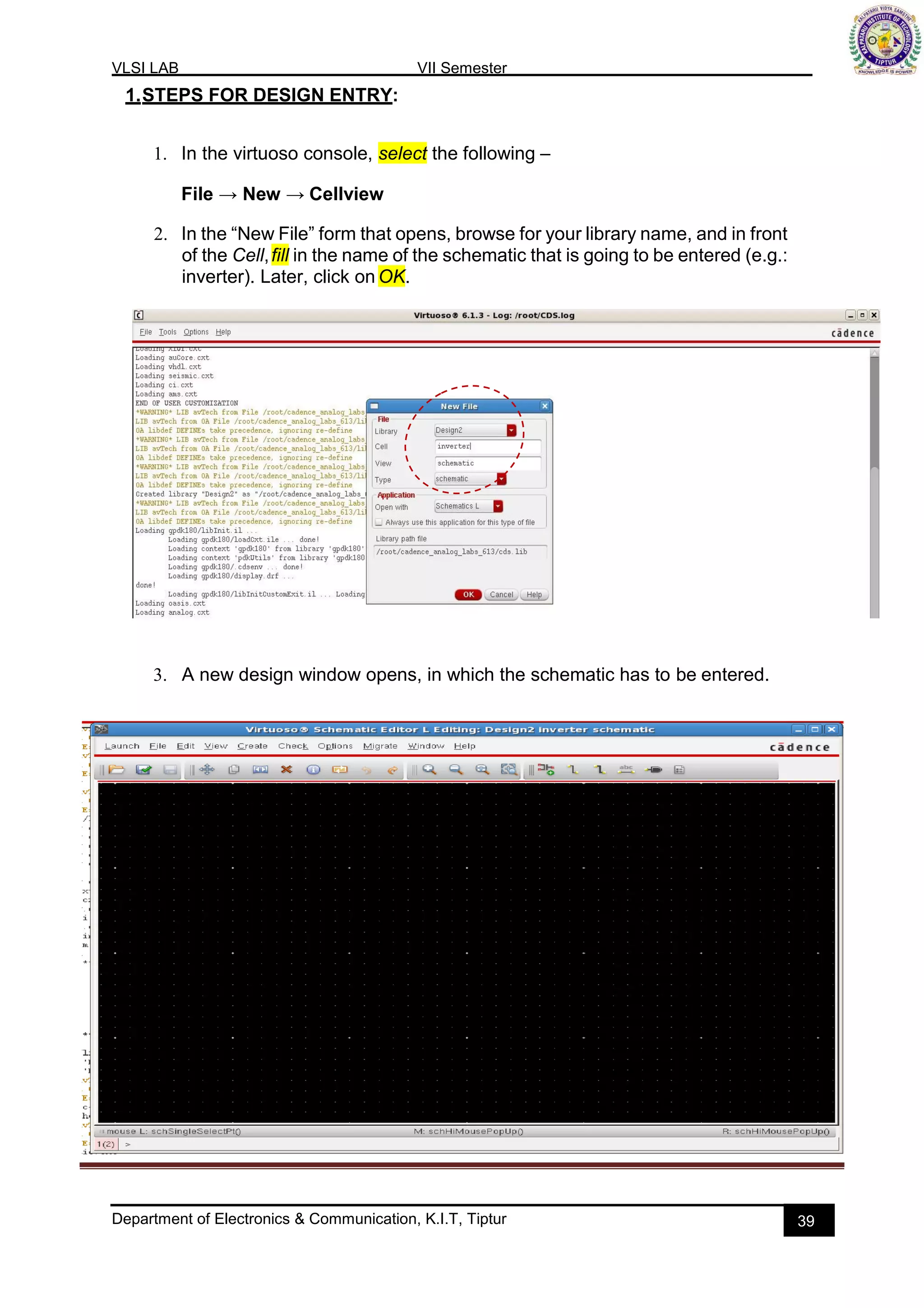
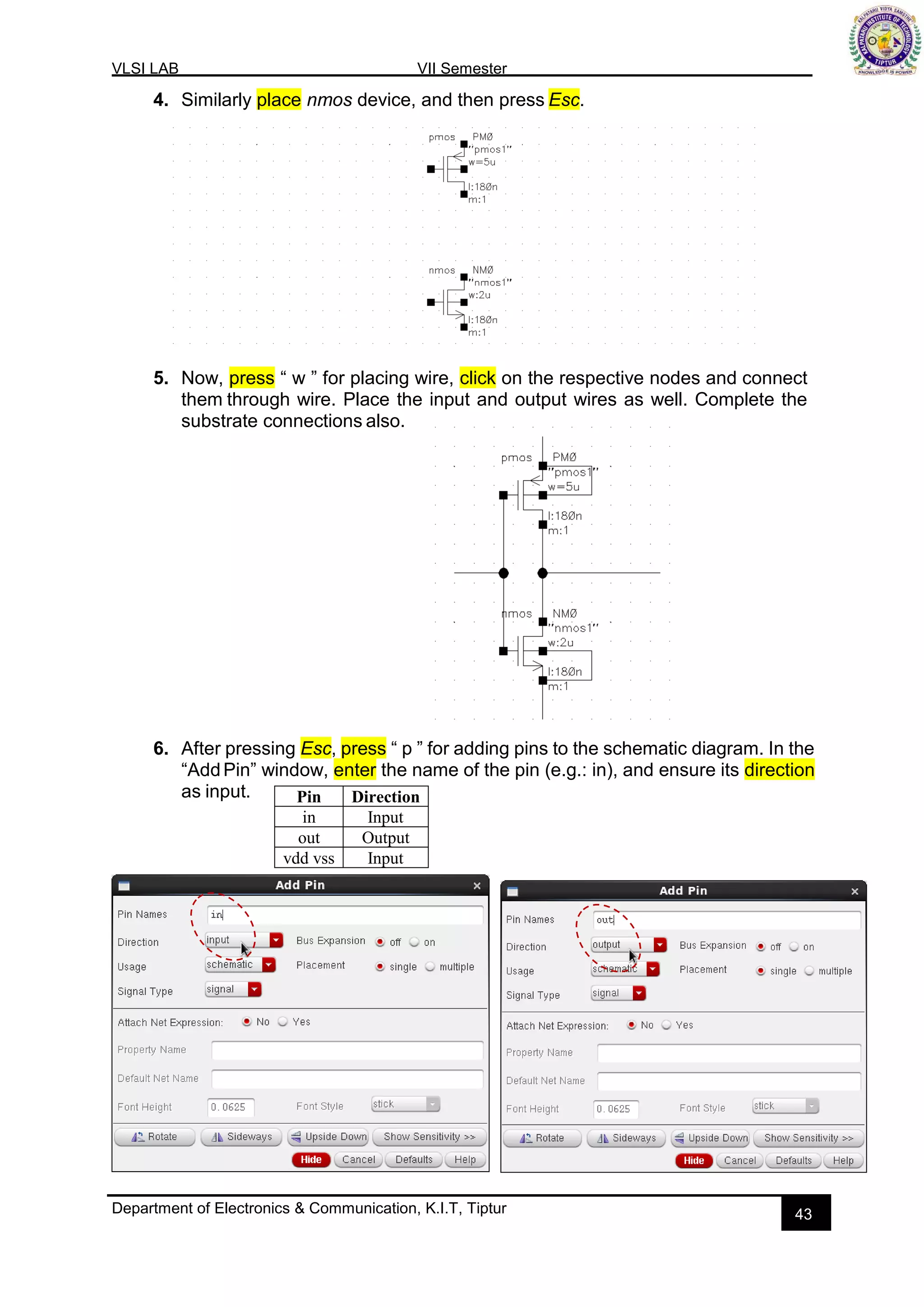
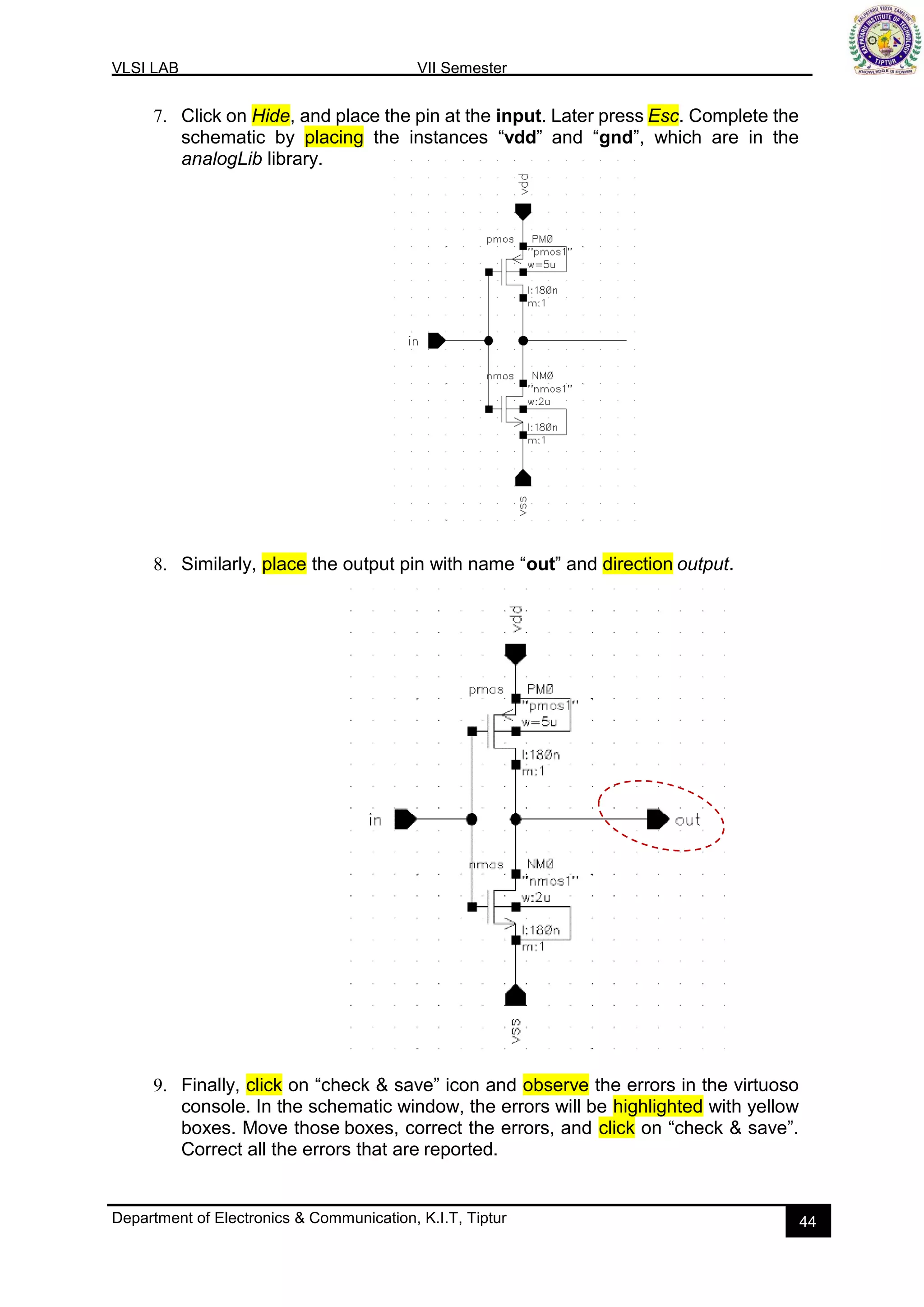
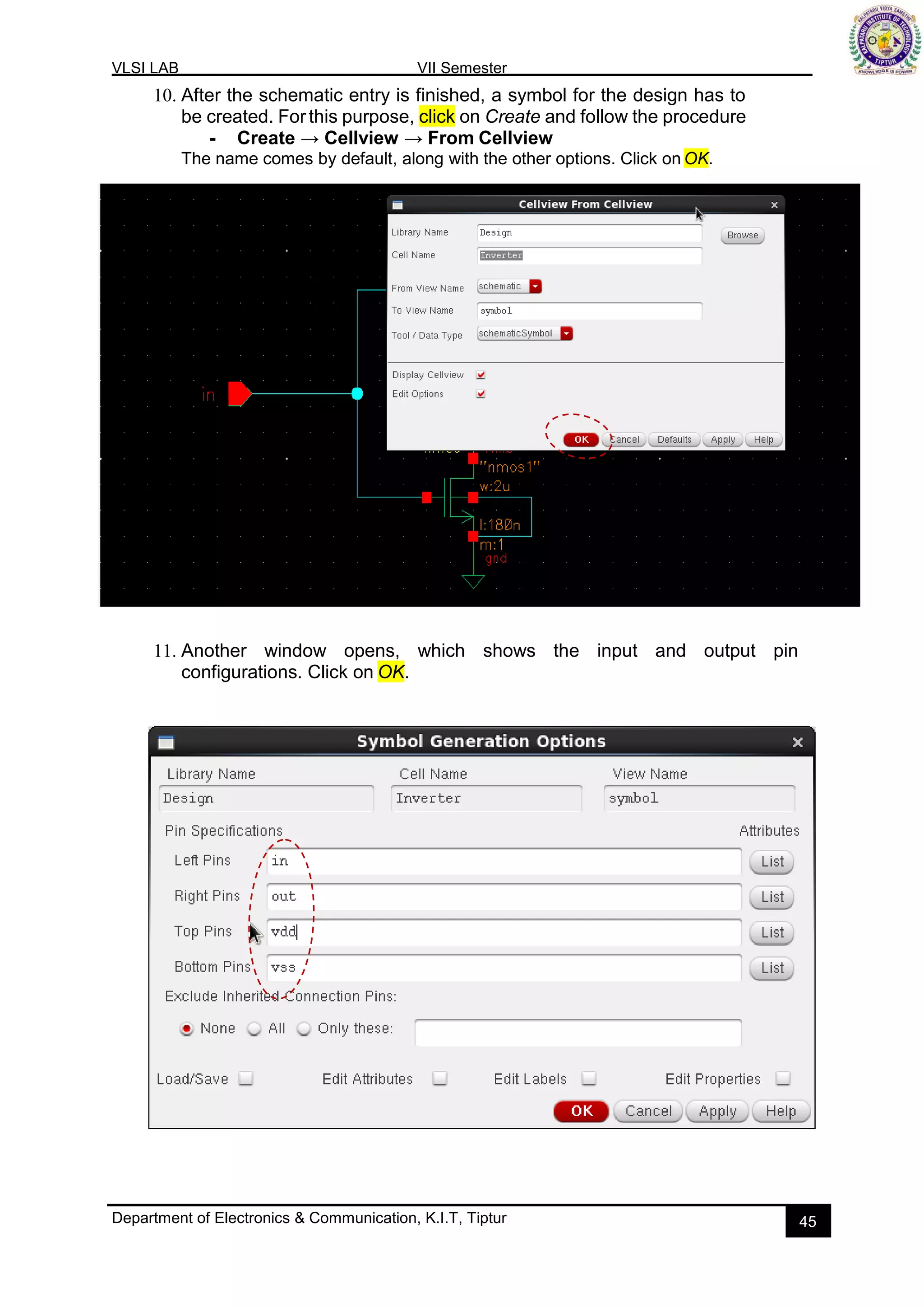
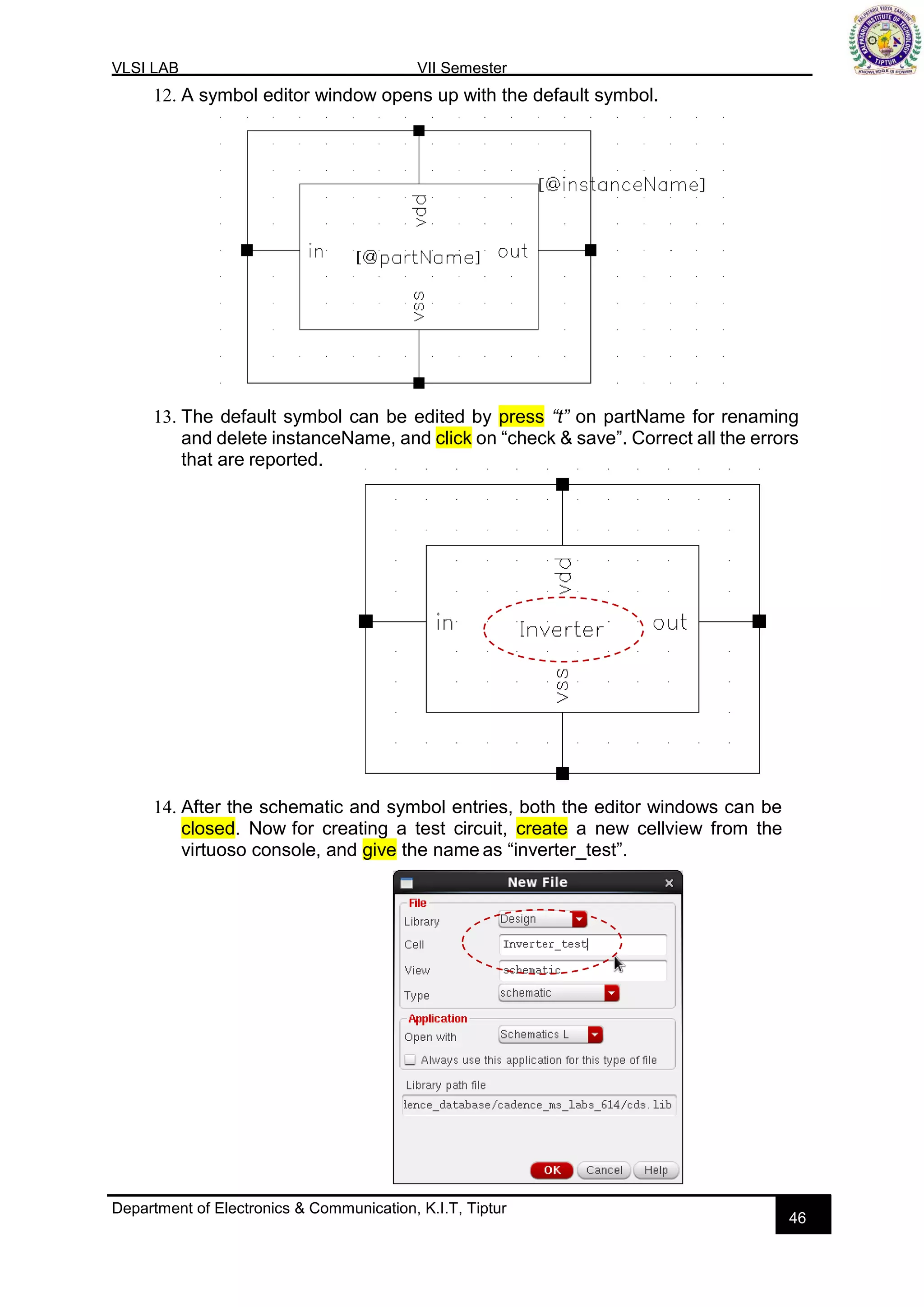
This document provides information about VLSI design procedures for an analog design flow. It includes details on initial procedures for using Cadence tools, steps for design entry including schematic entry, symbol creation and test circuit creation. It also describes simulation procedures using ADE-L and layout procedures using Layout-XL. An example inverter design is provided with steps for schematic entry, simulation and layout. Key Cadence tools used are listed as Virtuoso schematic editor, ADE-L, Spectre and Virtuoso layout suite.
Introduction to nanoLambda, MEMsim, PROtutor and size comparison of 45nm technology.
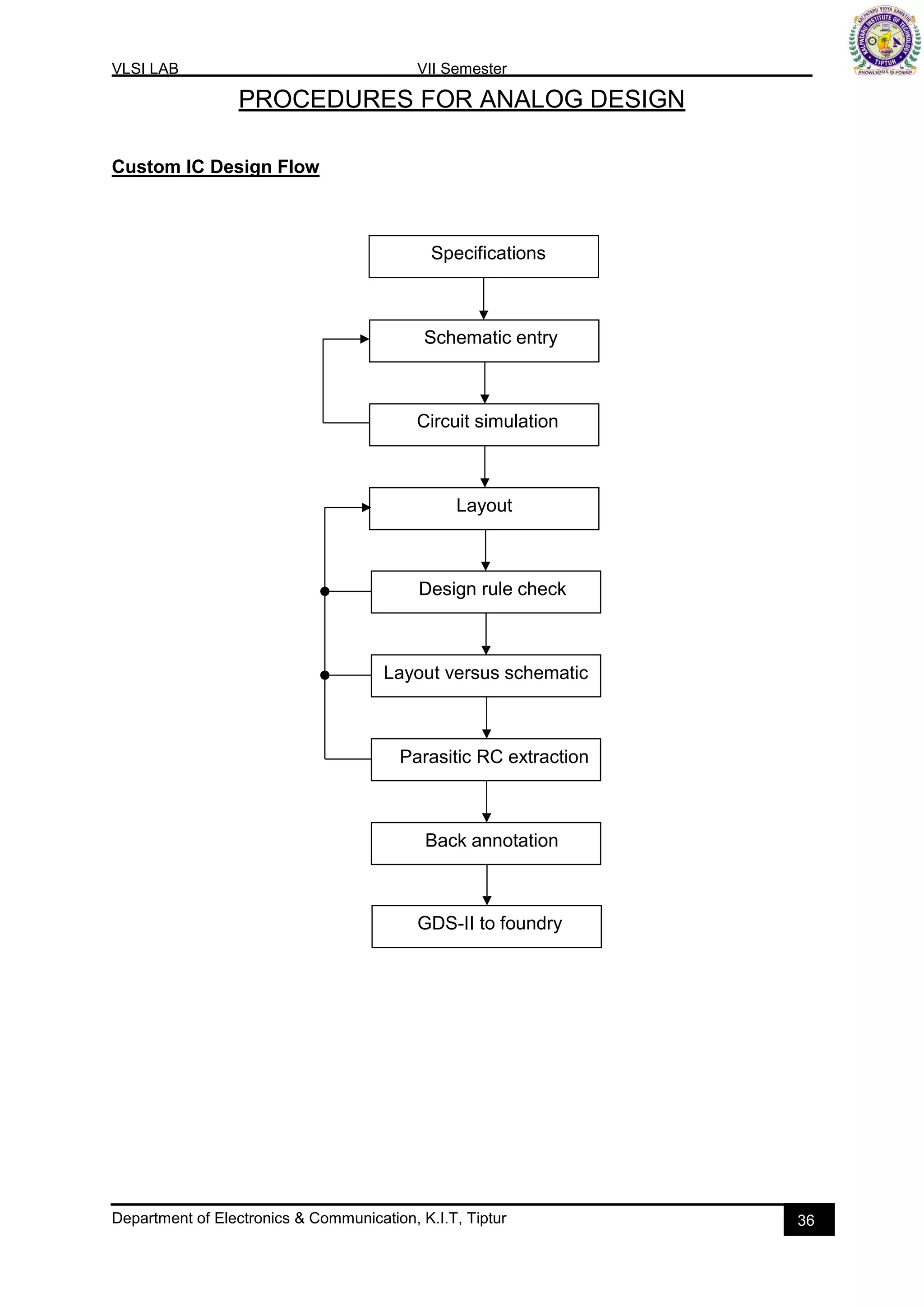
Procedures for analog design including circuit simulation, schematic entry, layout, and specifications.
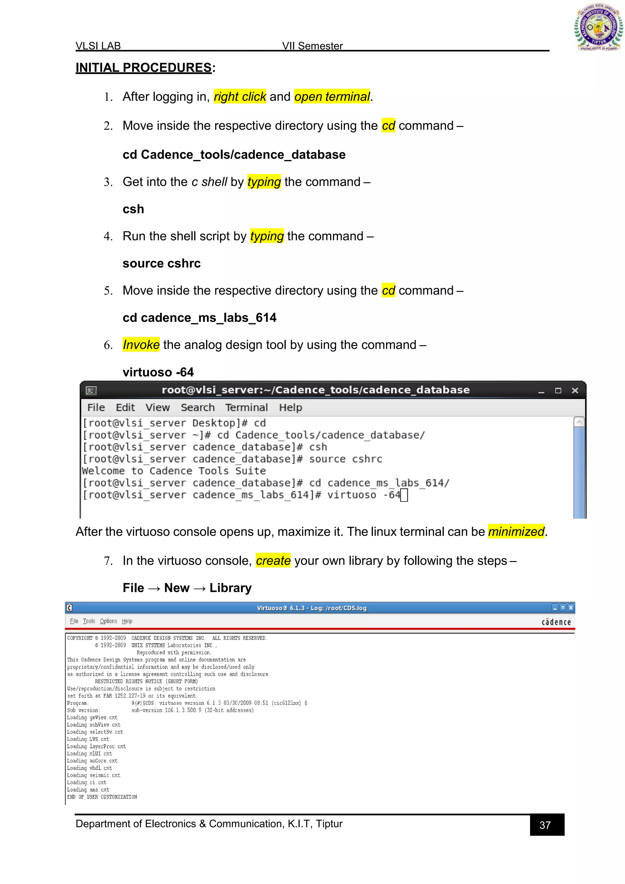
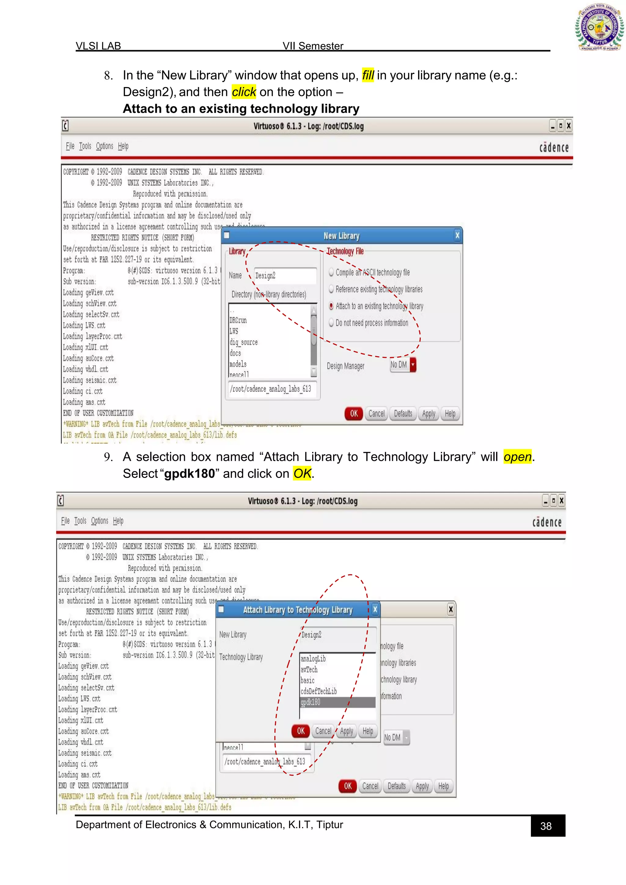
Step-by-step login to the system, directory navigation, and invoking the analog design tool.
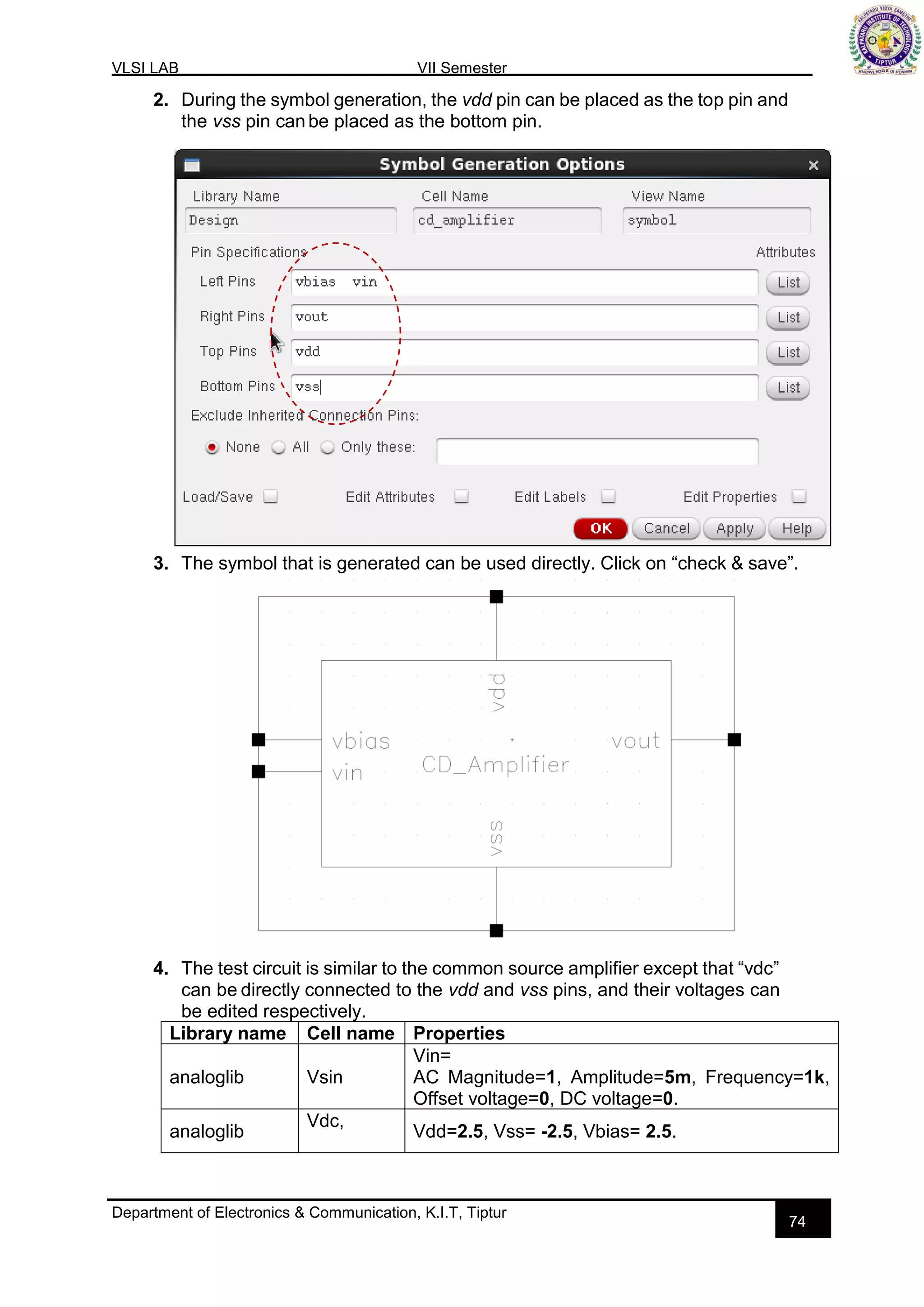
Procedure for design entry, including schematic creation, symbol creation, and simulation steps.
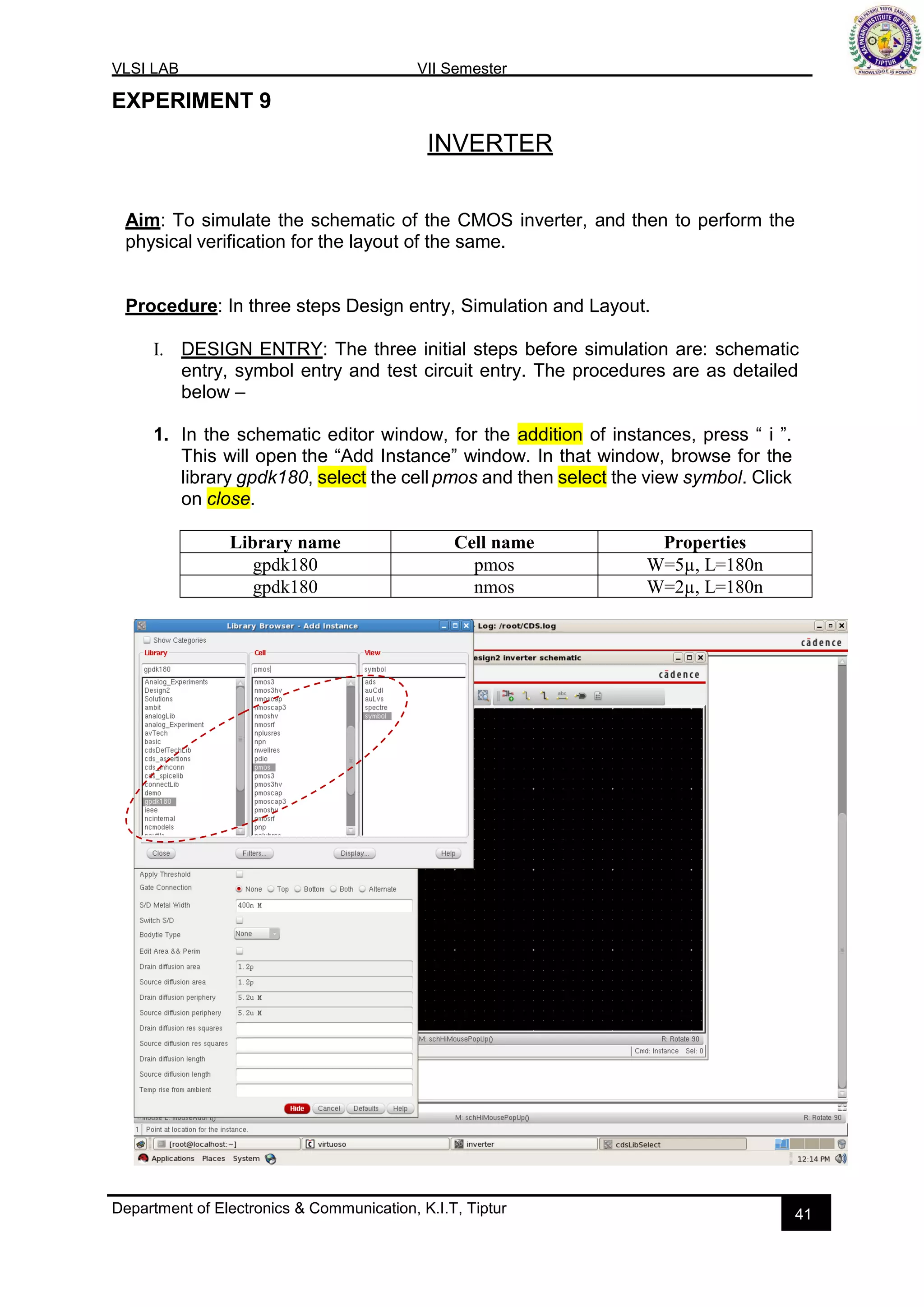
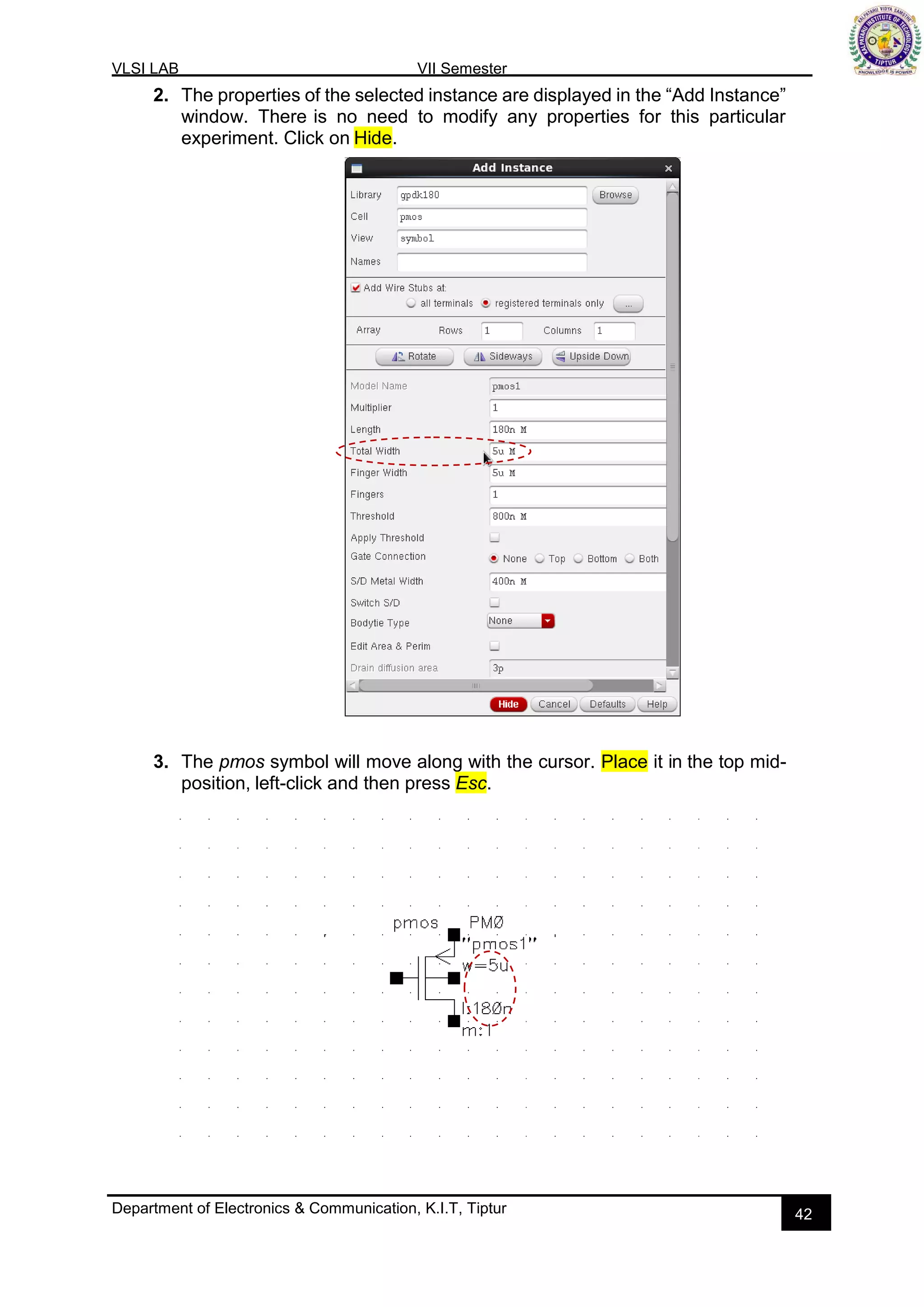
Details and procedures for simulating a CMOS inverter design, including instance selection and schematic completion.
Finalizing inverter's schematic and symbol entries, detailing test circuit creation and settings for simulation.
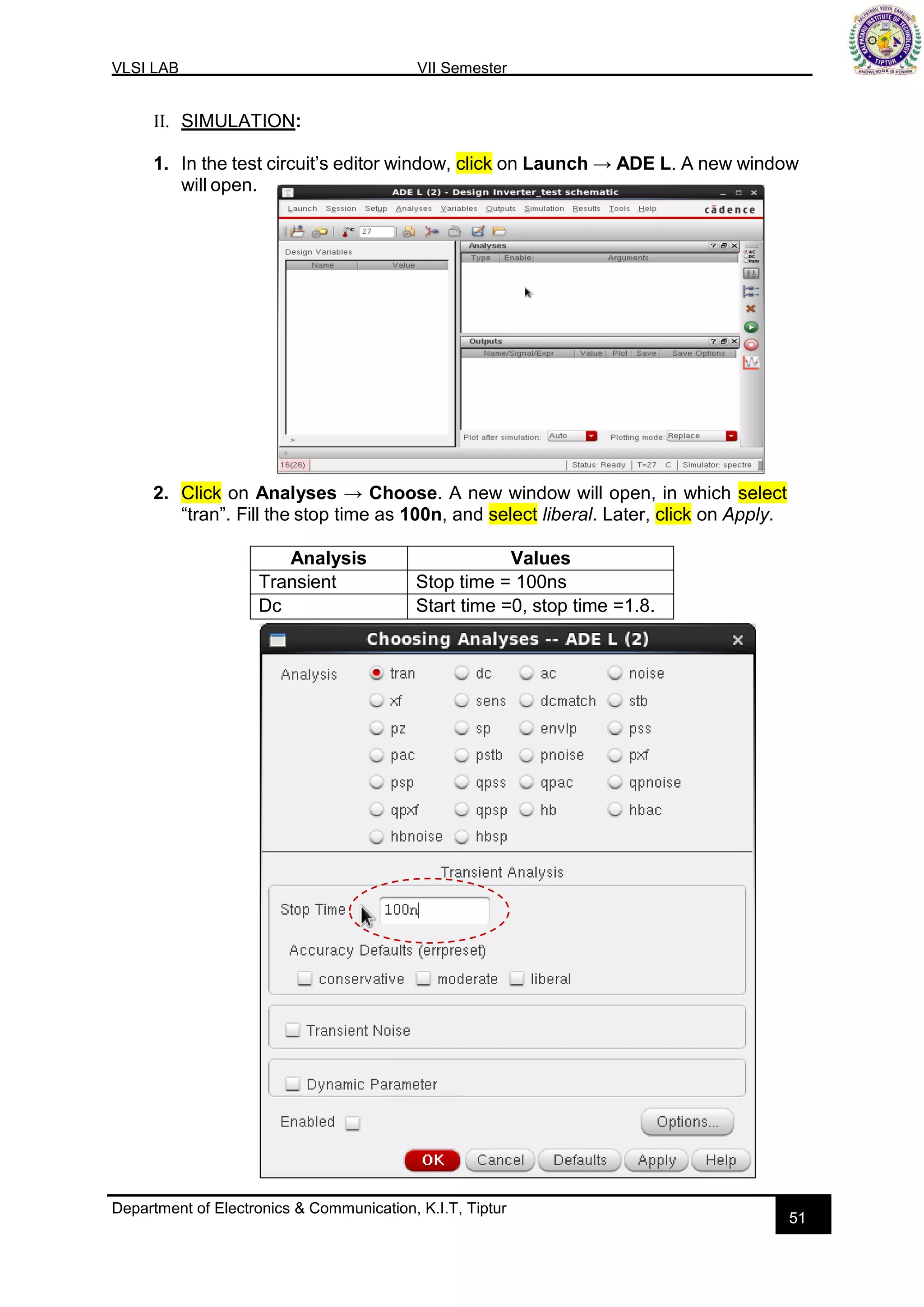
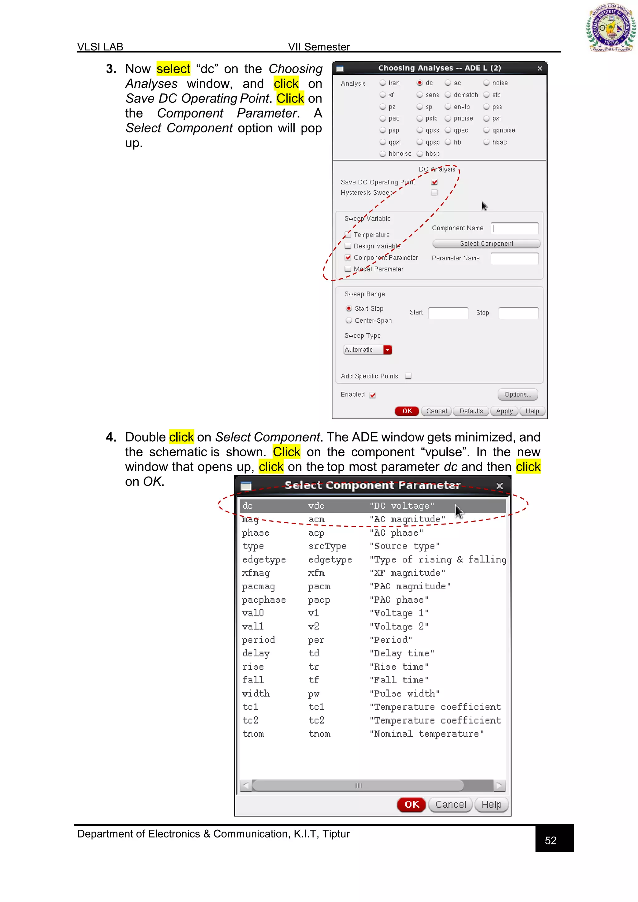
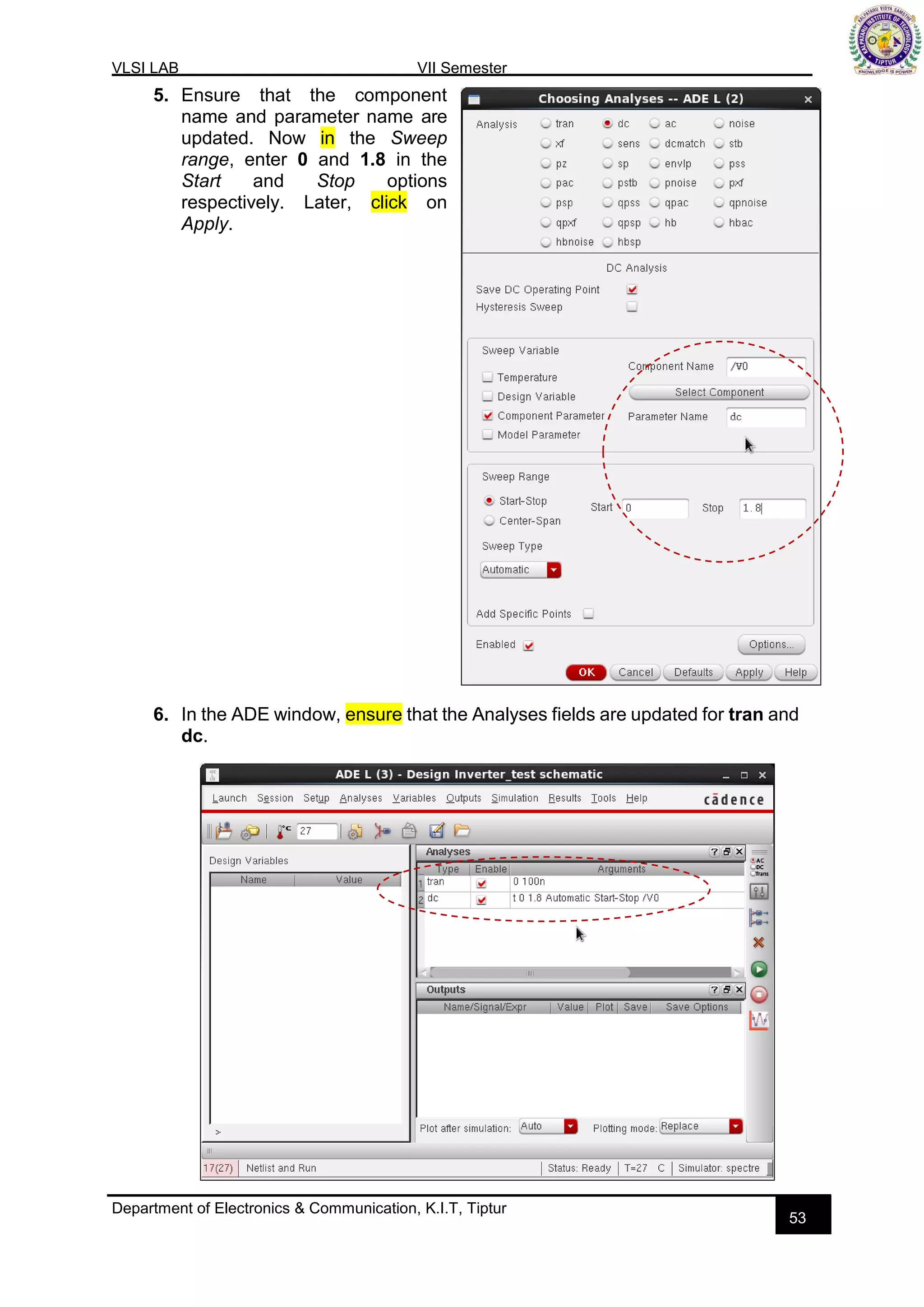
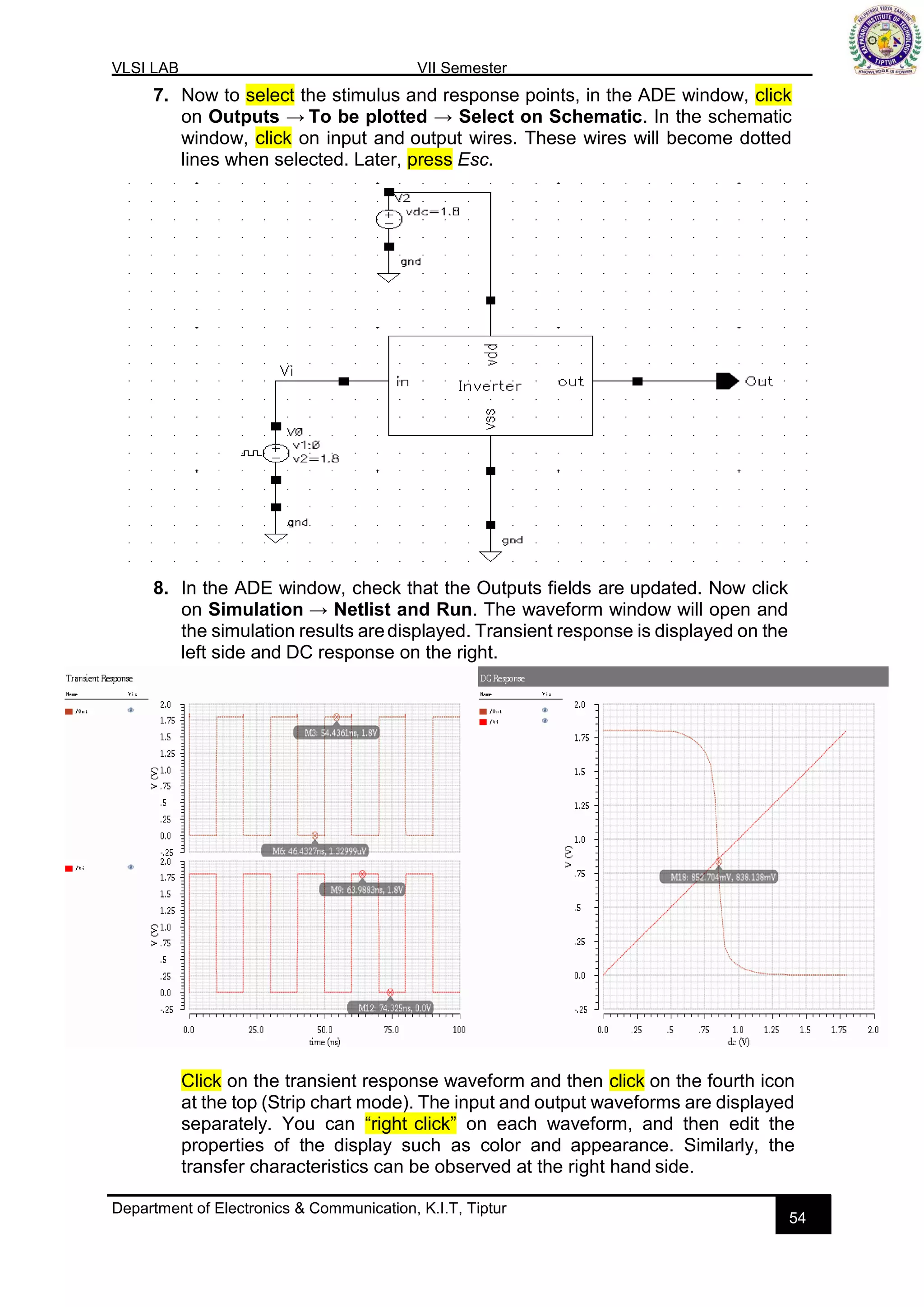
Instruction for launching simulations in ADE-L, selecting analyses types, and running the simulations.
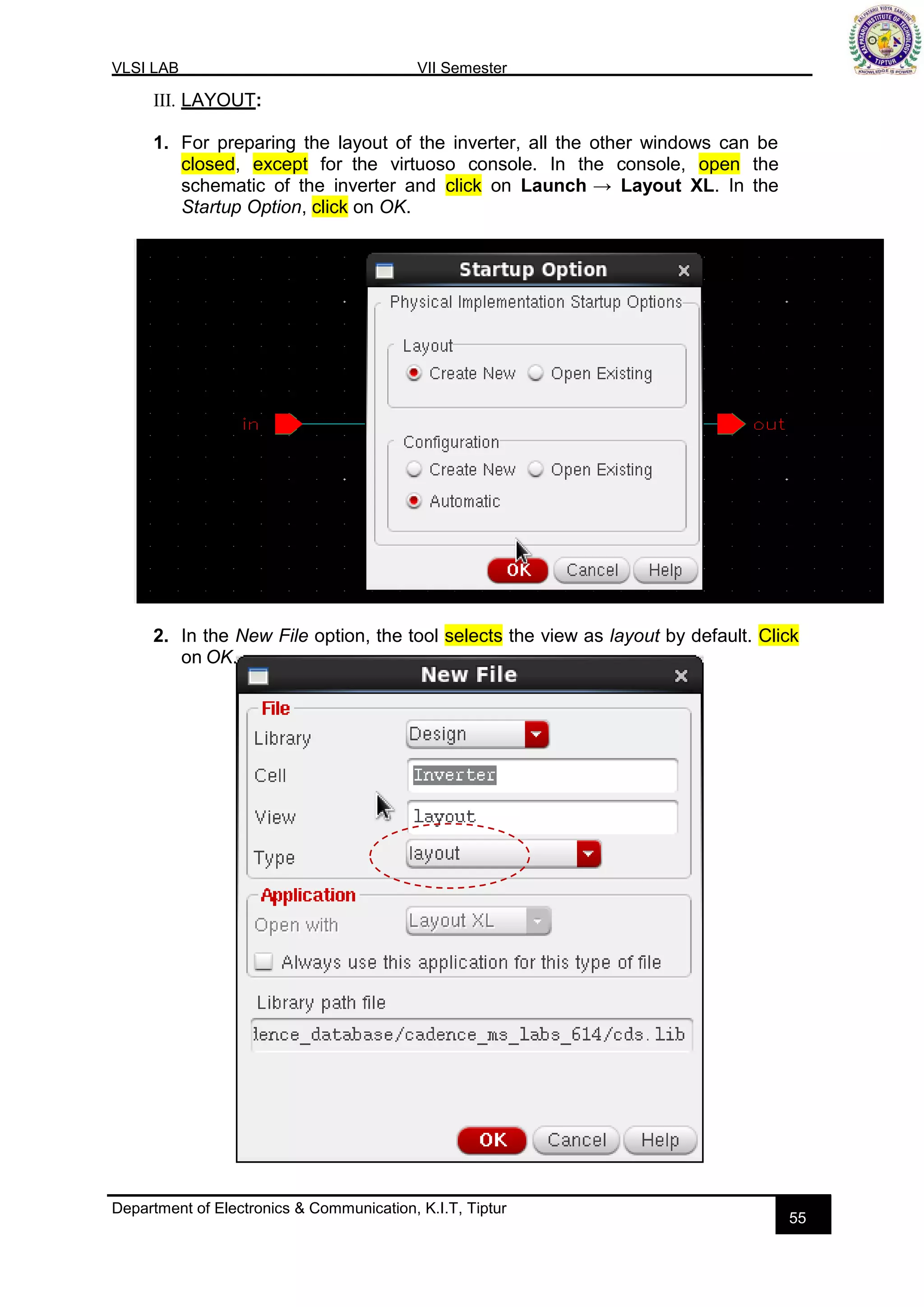
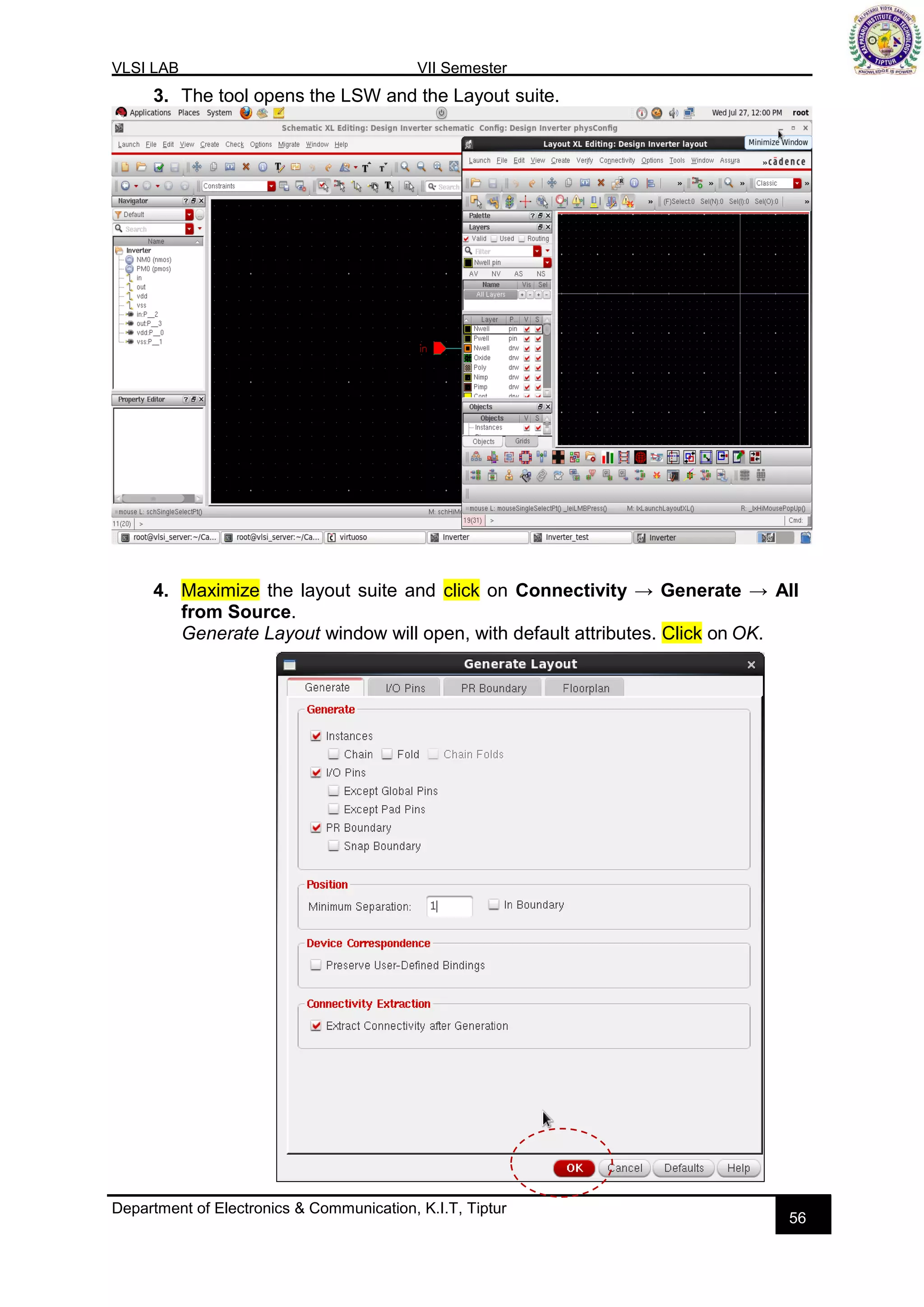
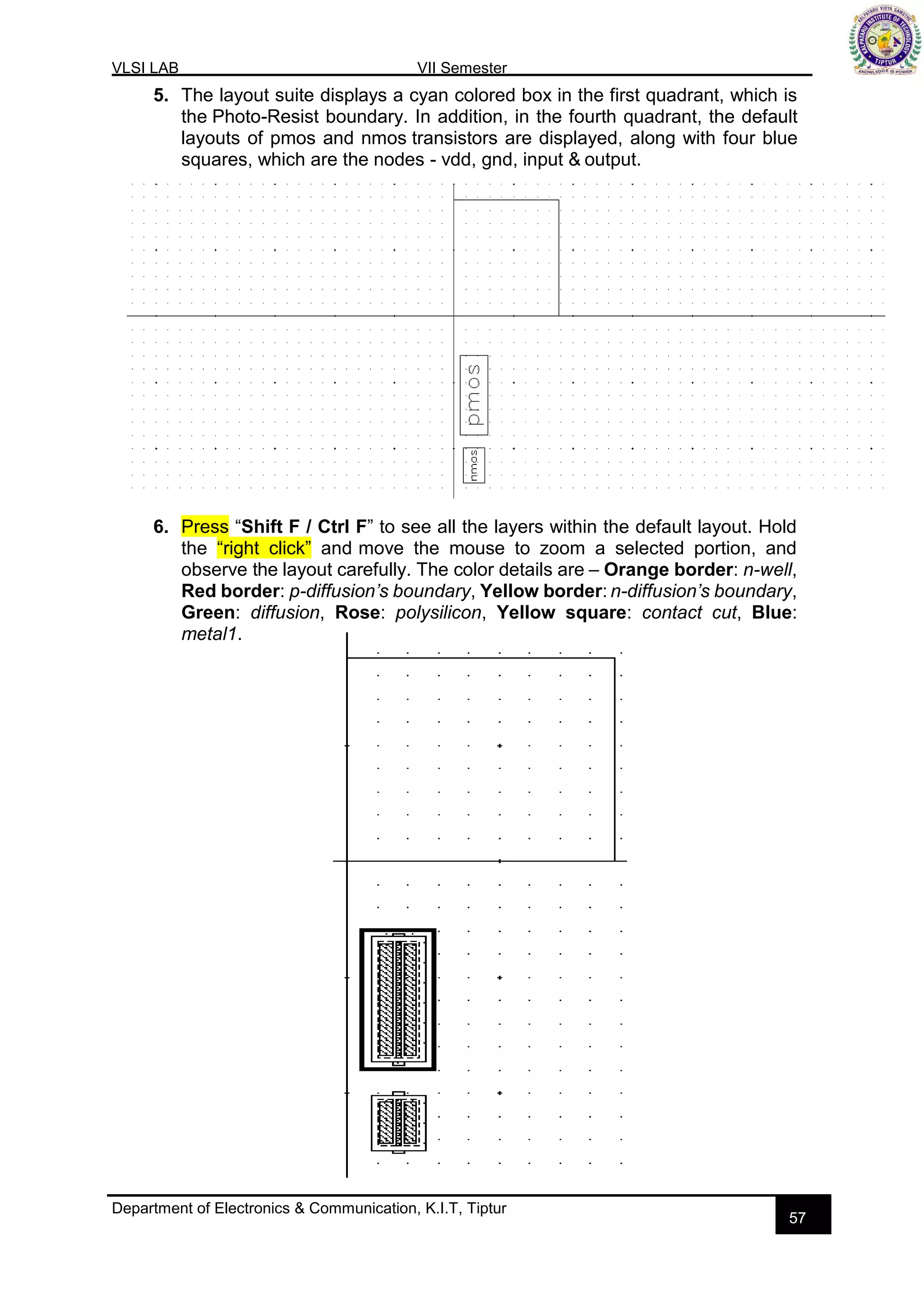
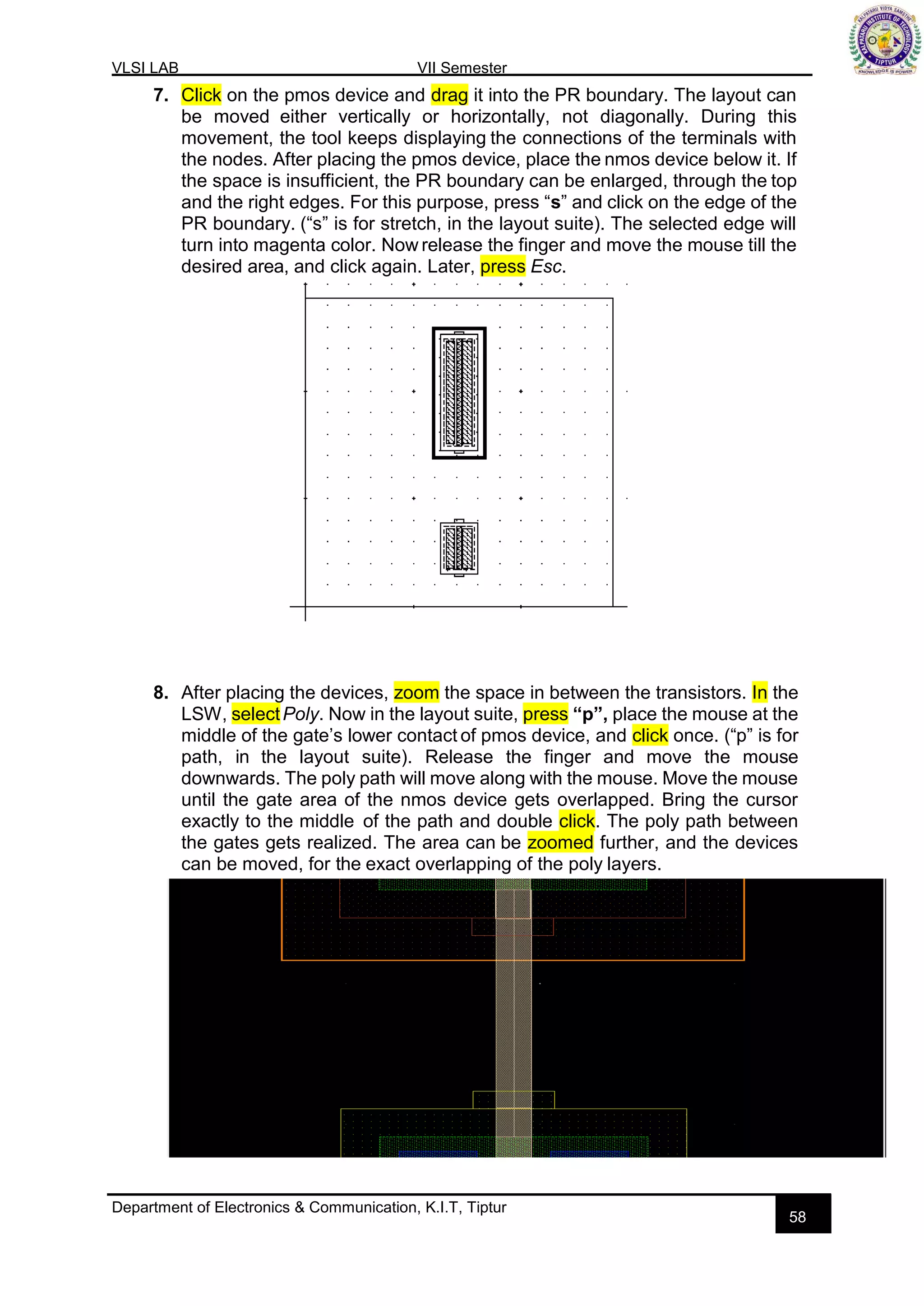
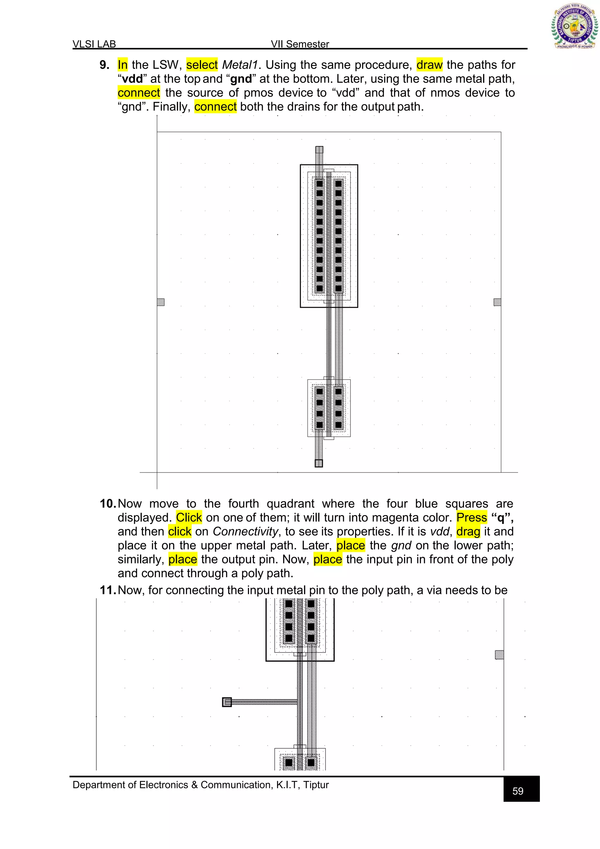
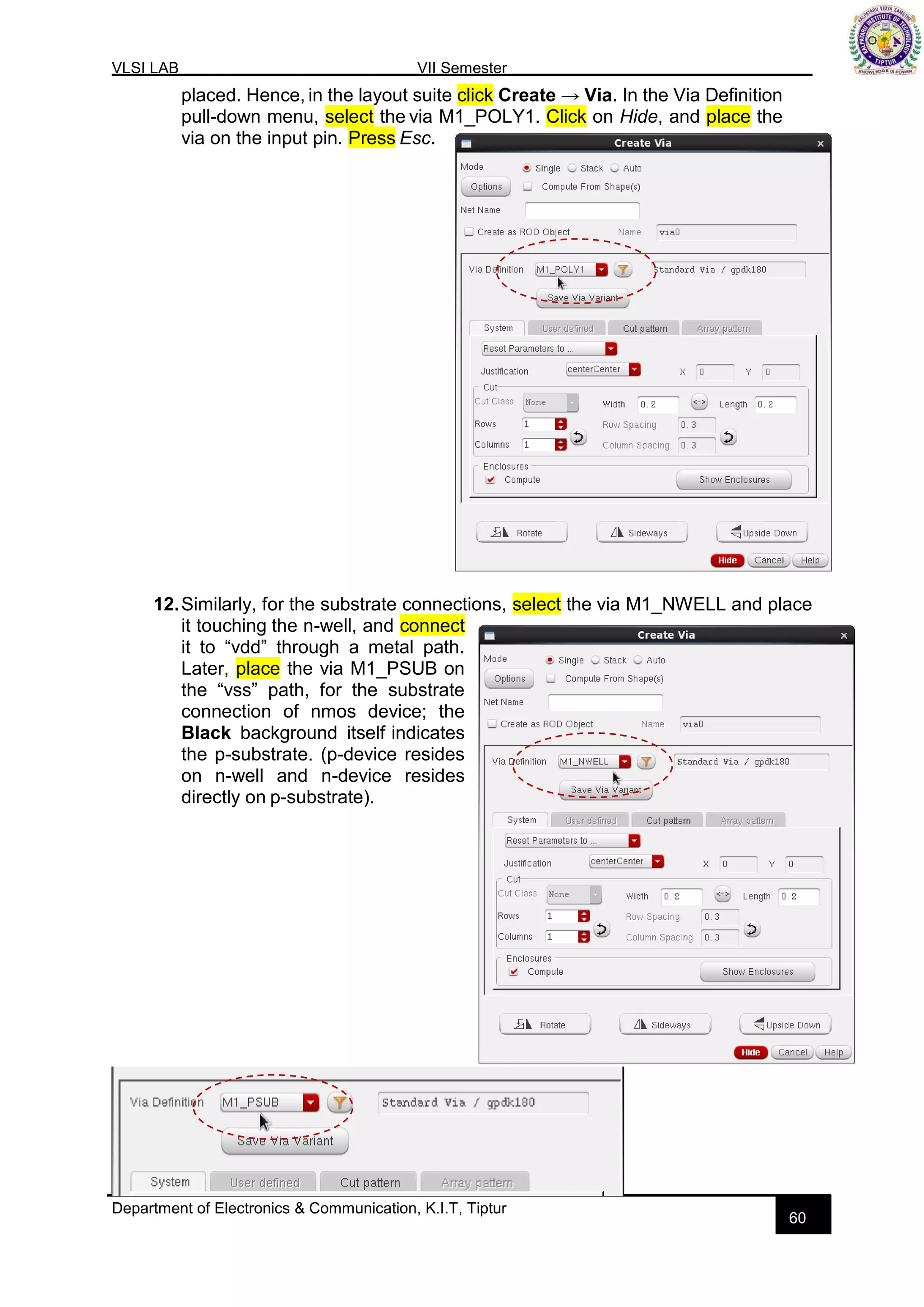
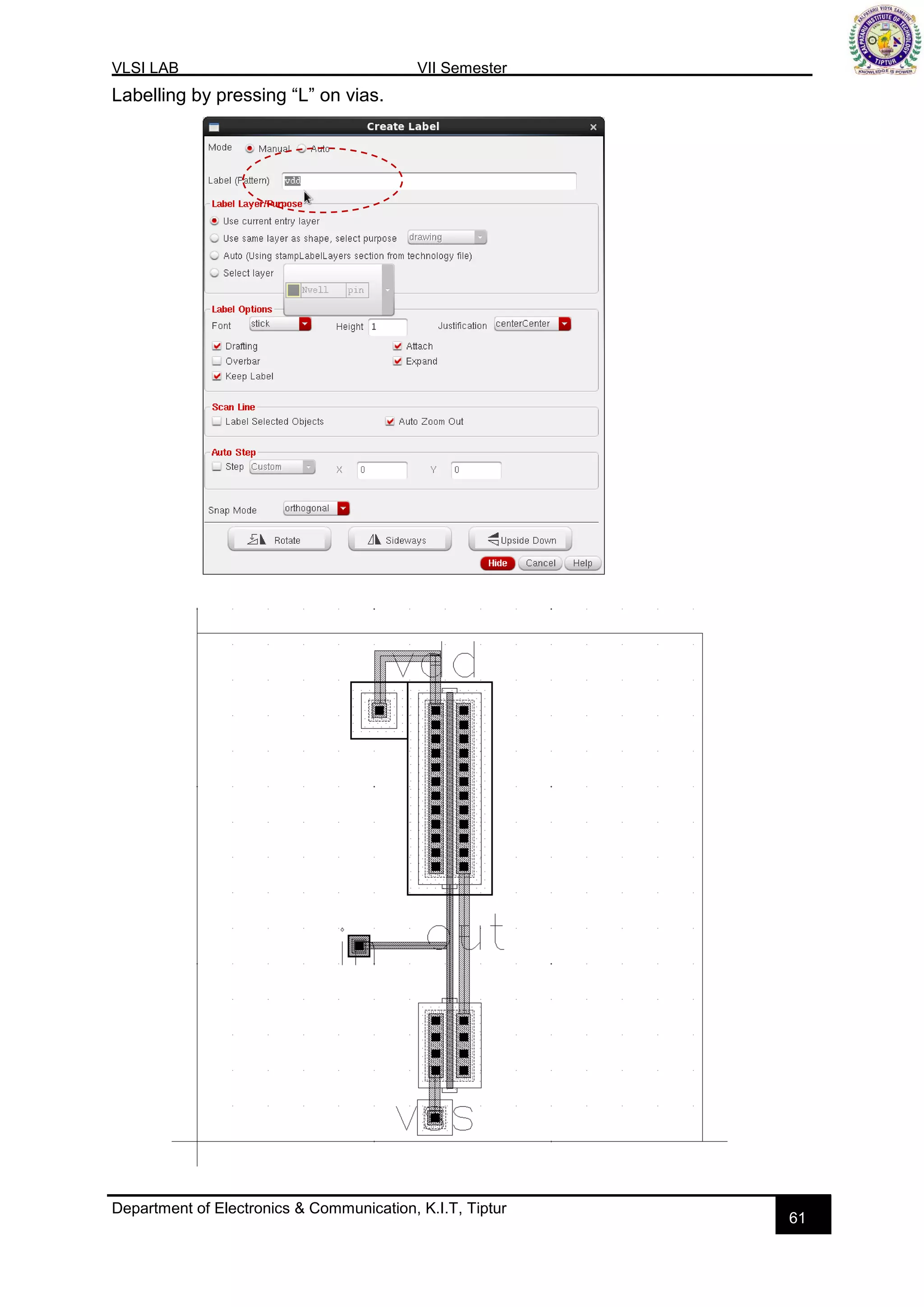
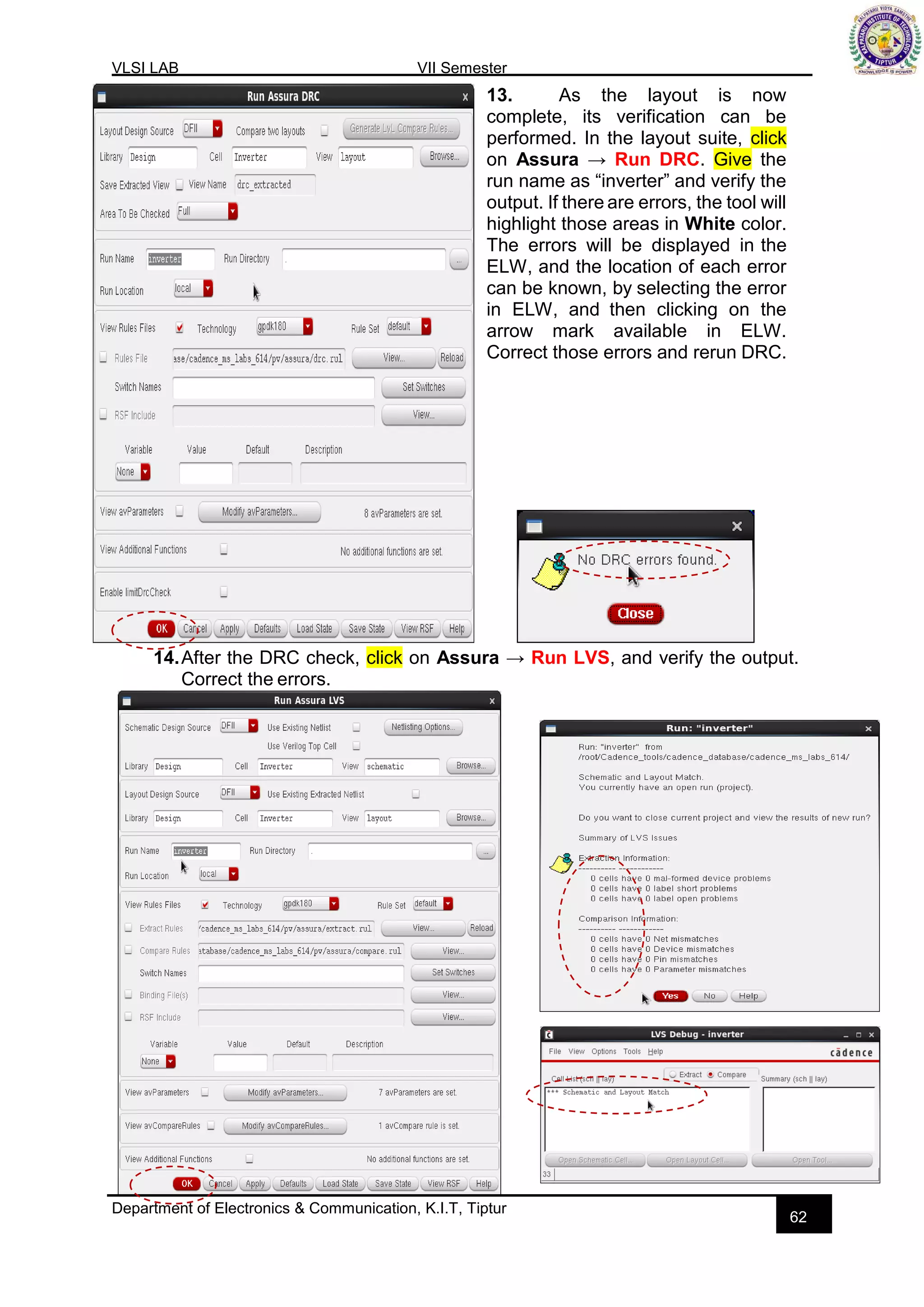
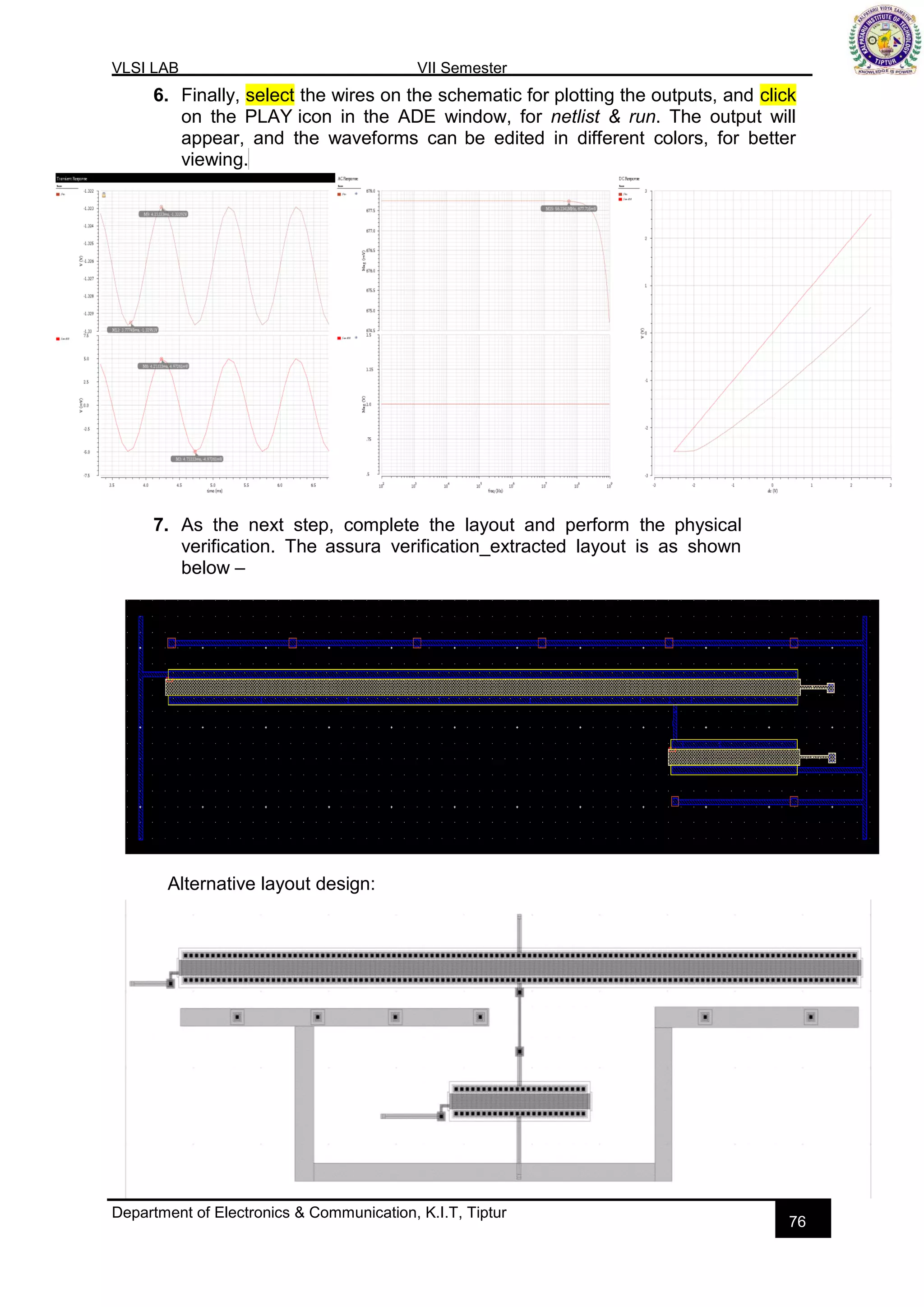
Steps for creating the physical layout of the inverter, including connectivity generation and verification steps.
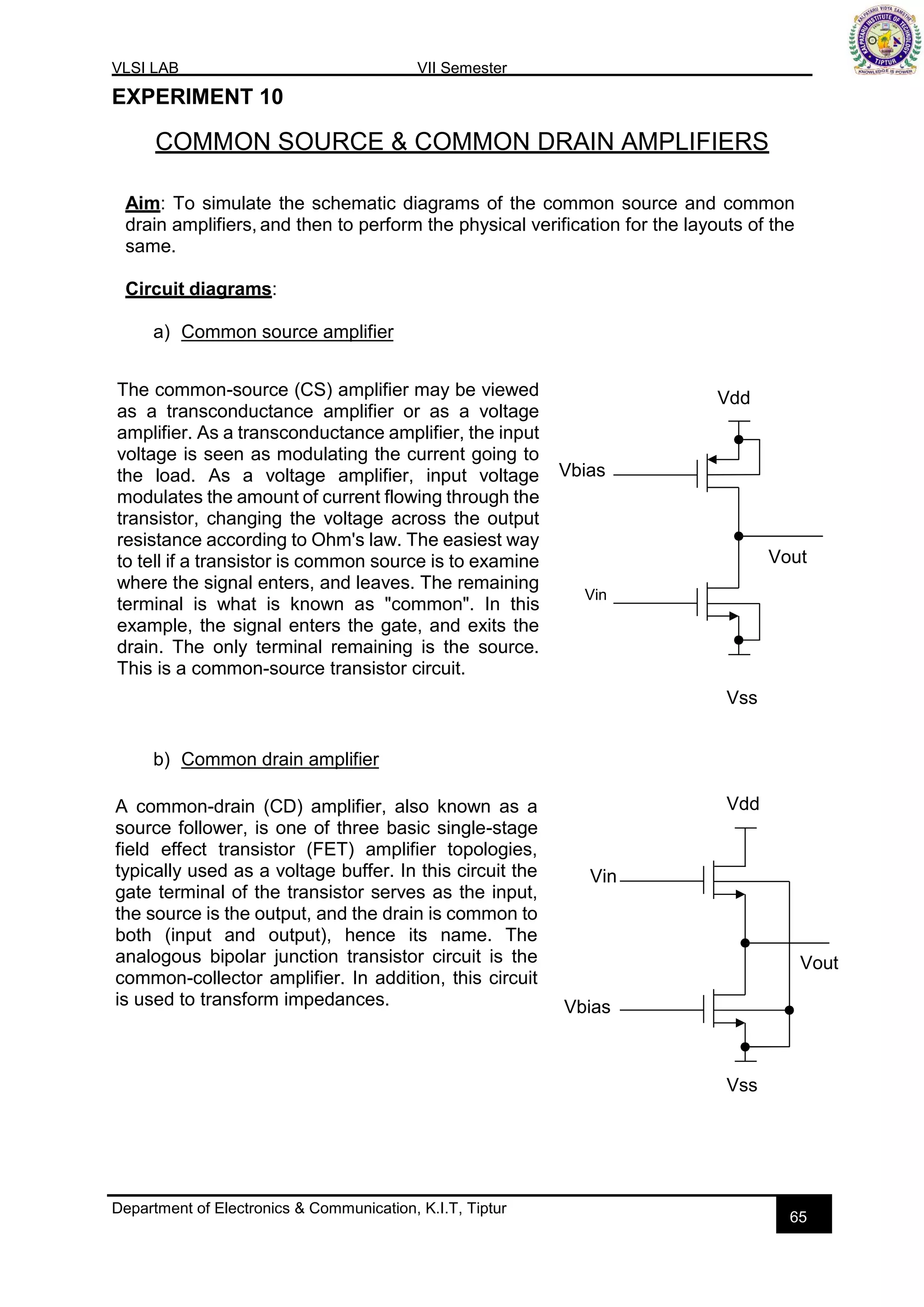
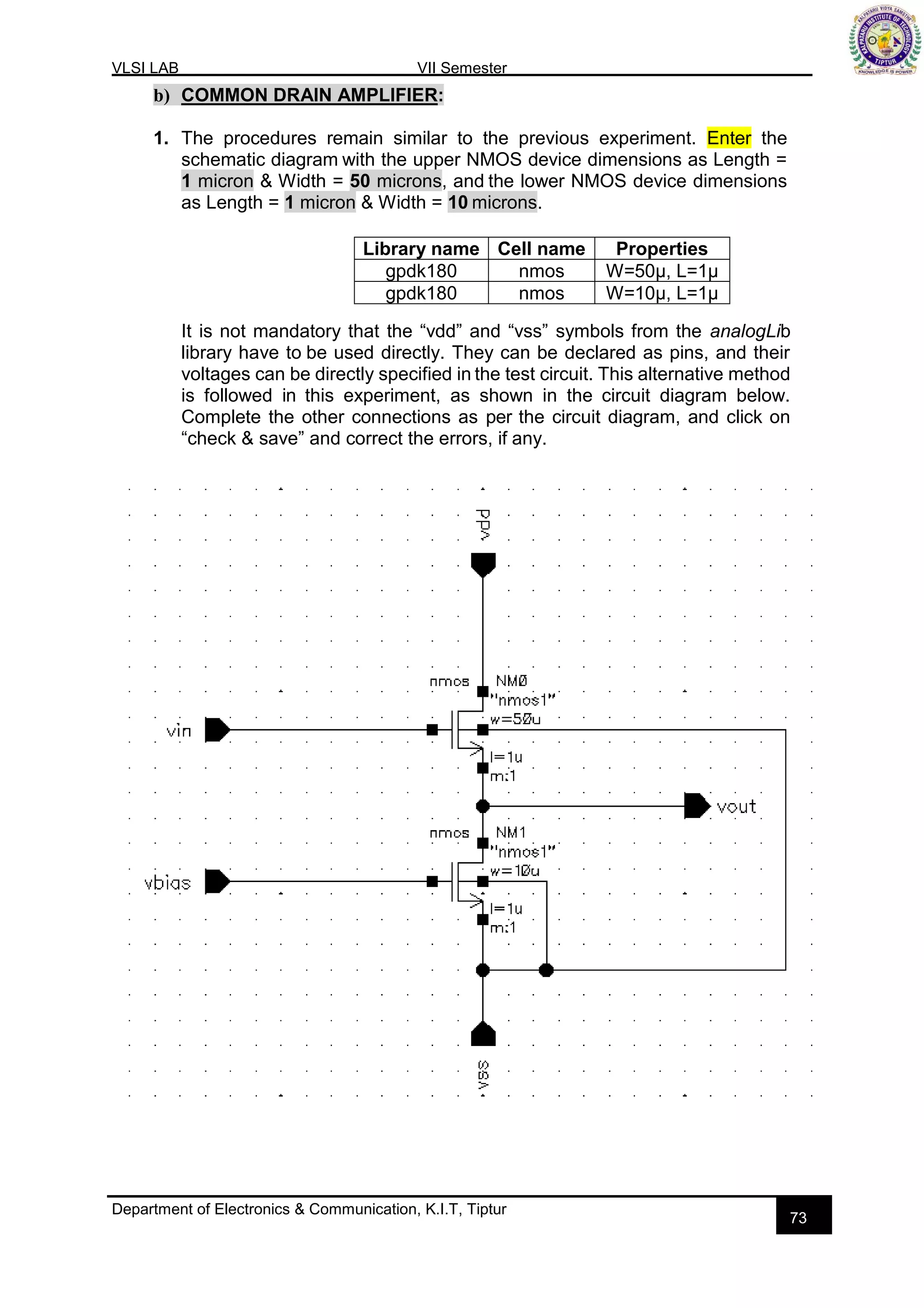
Introduction to amplifiers, schematic design requirements, and procedures for simulation in VLSI Lab.
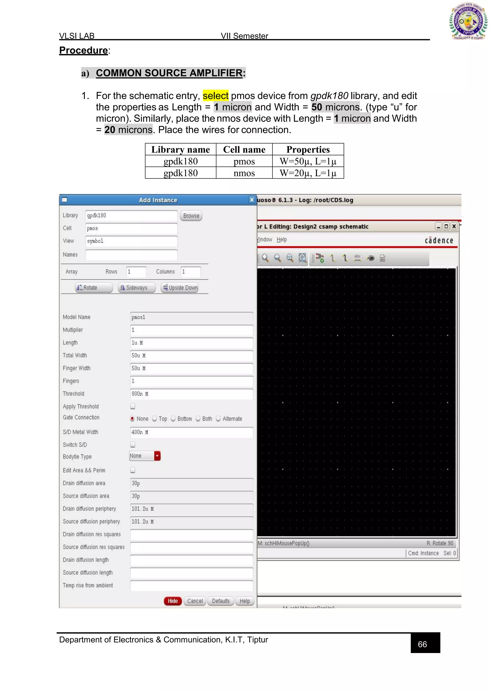
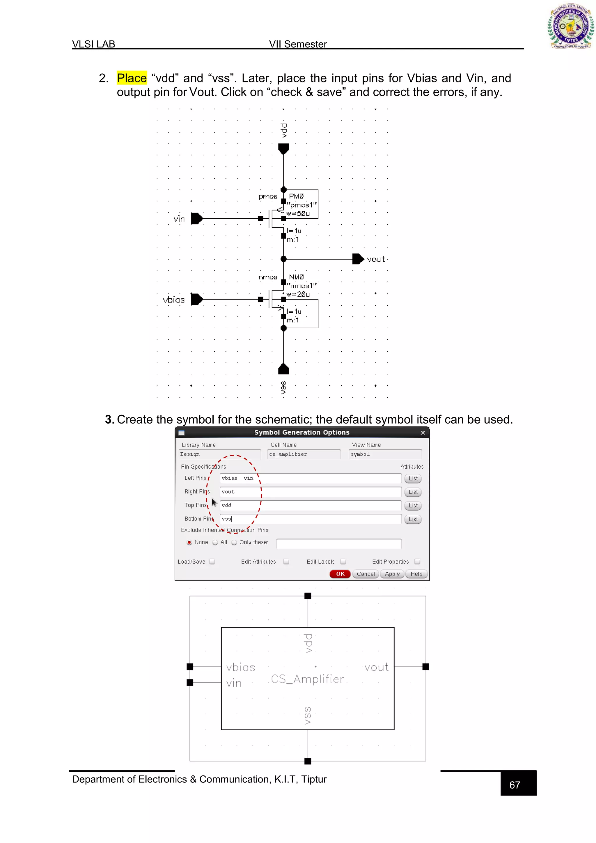
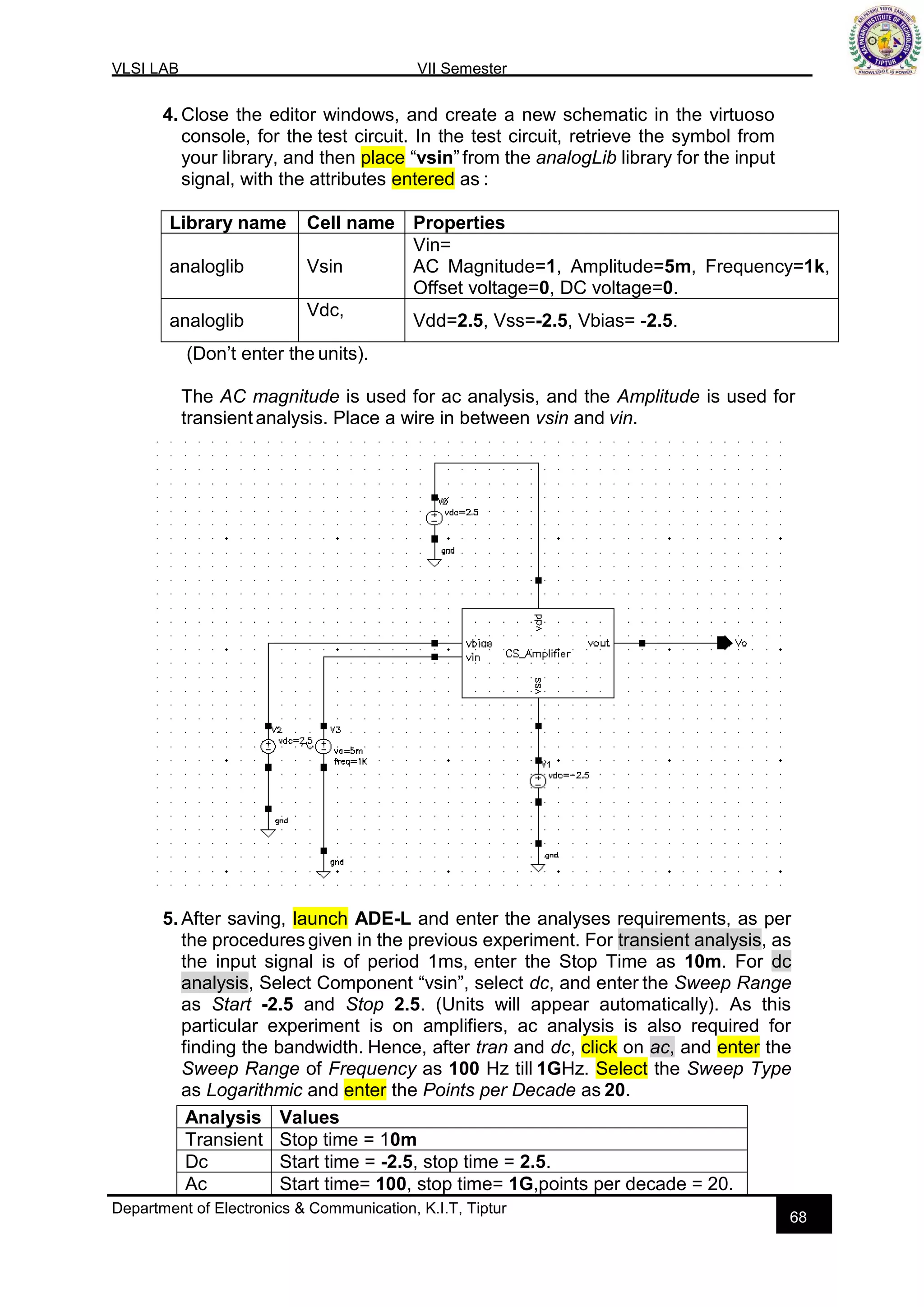
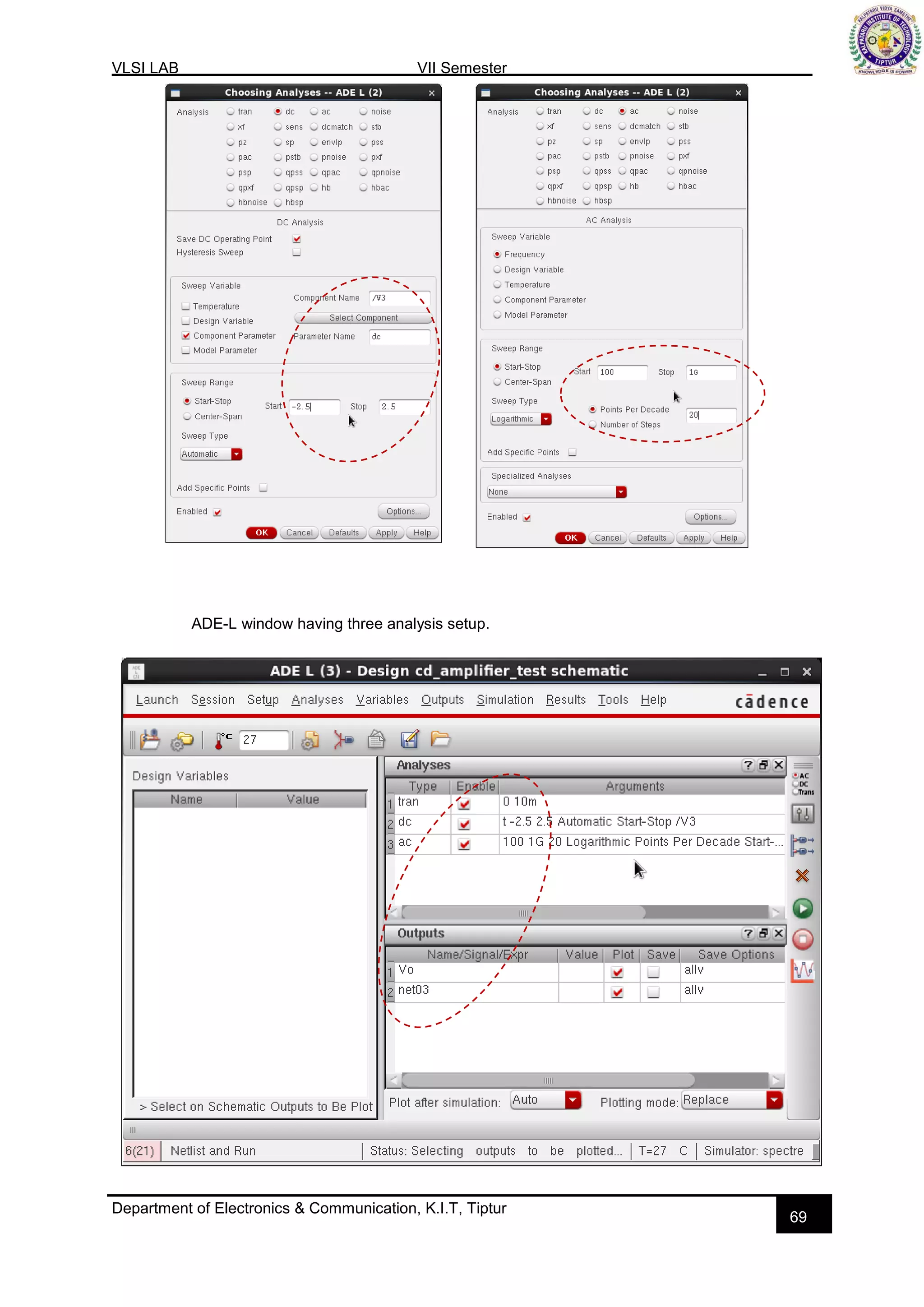
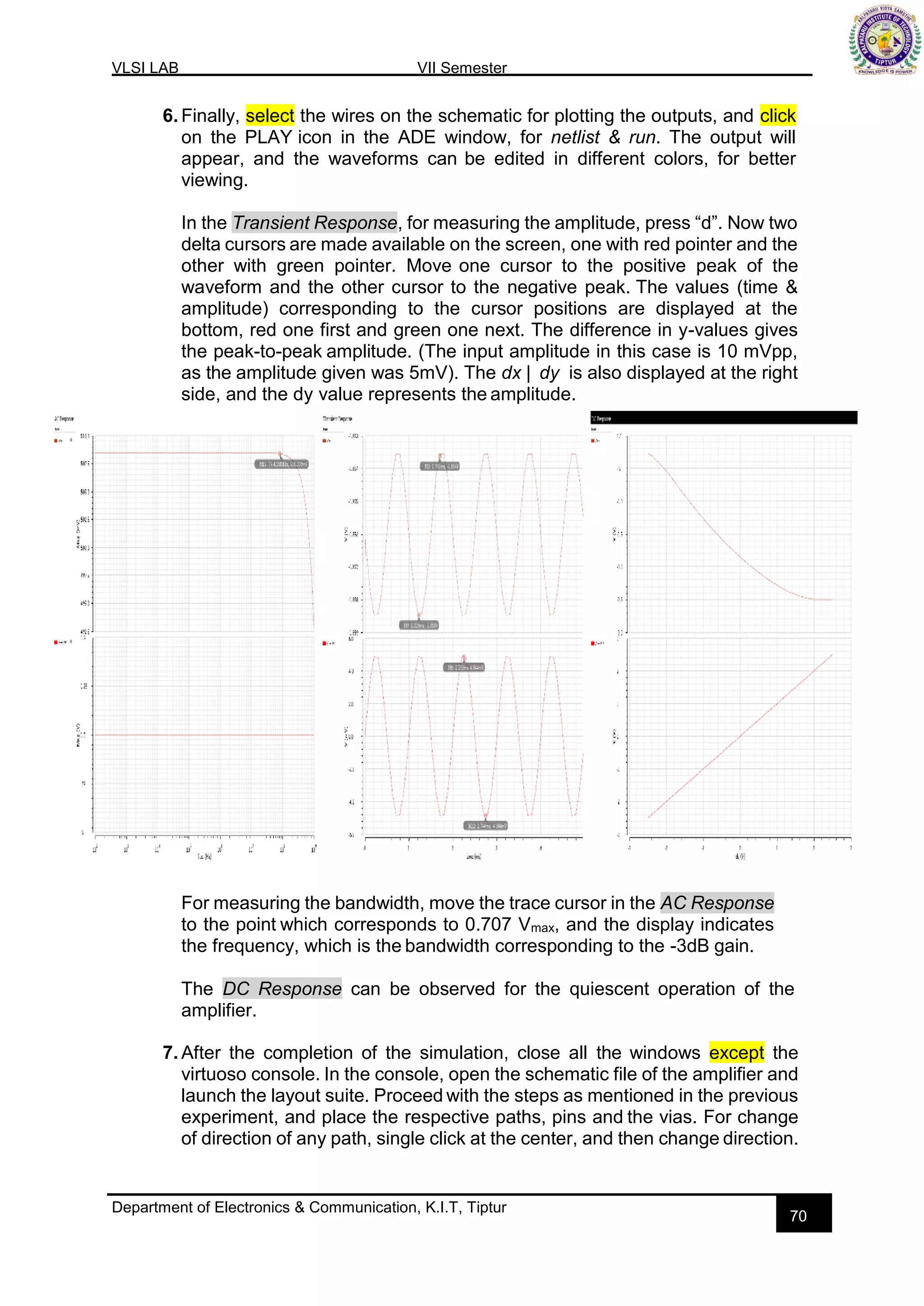
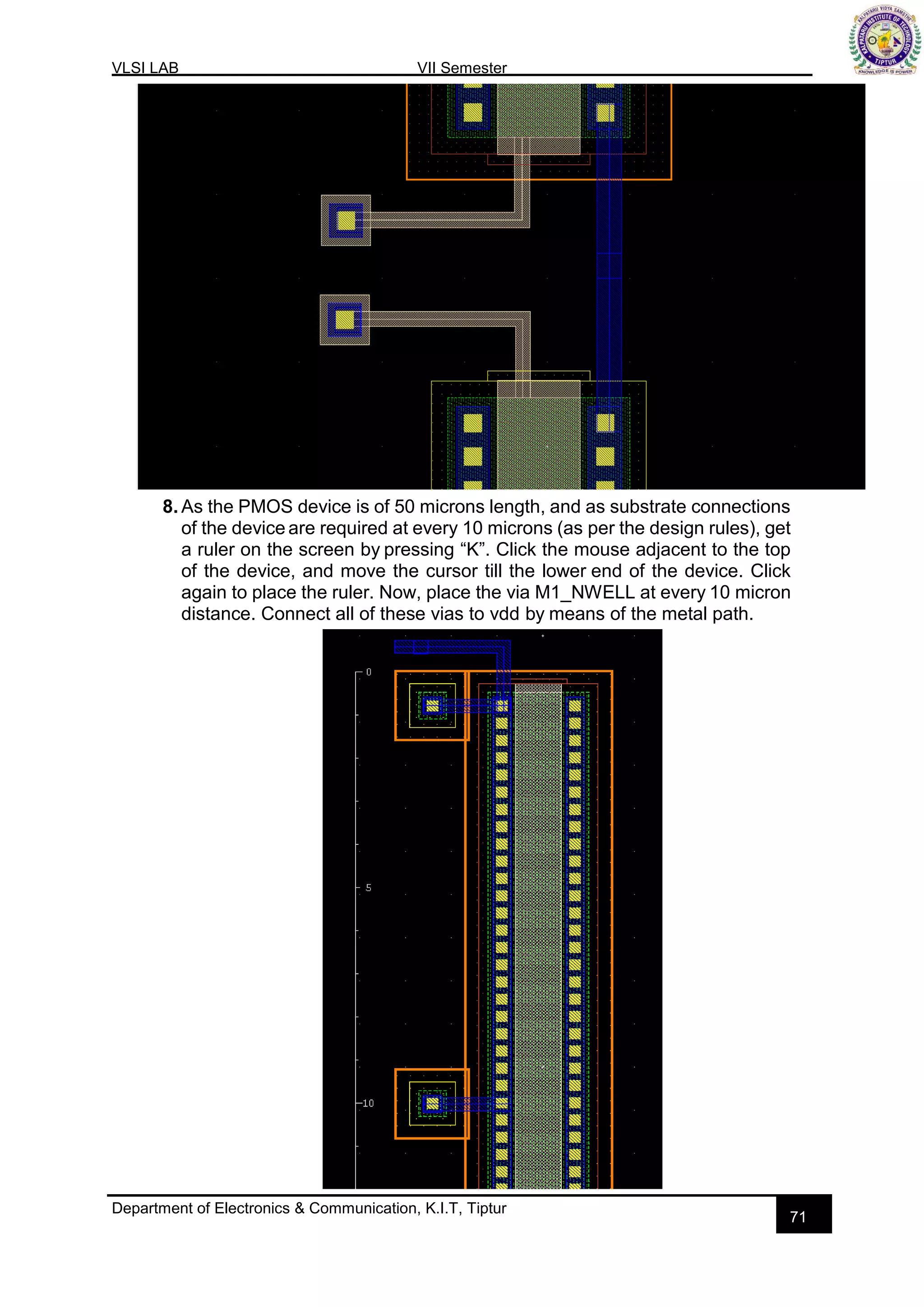
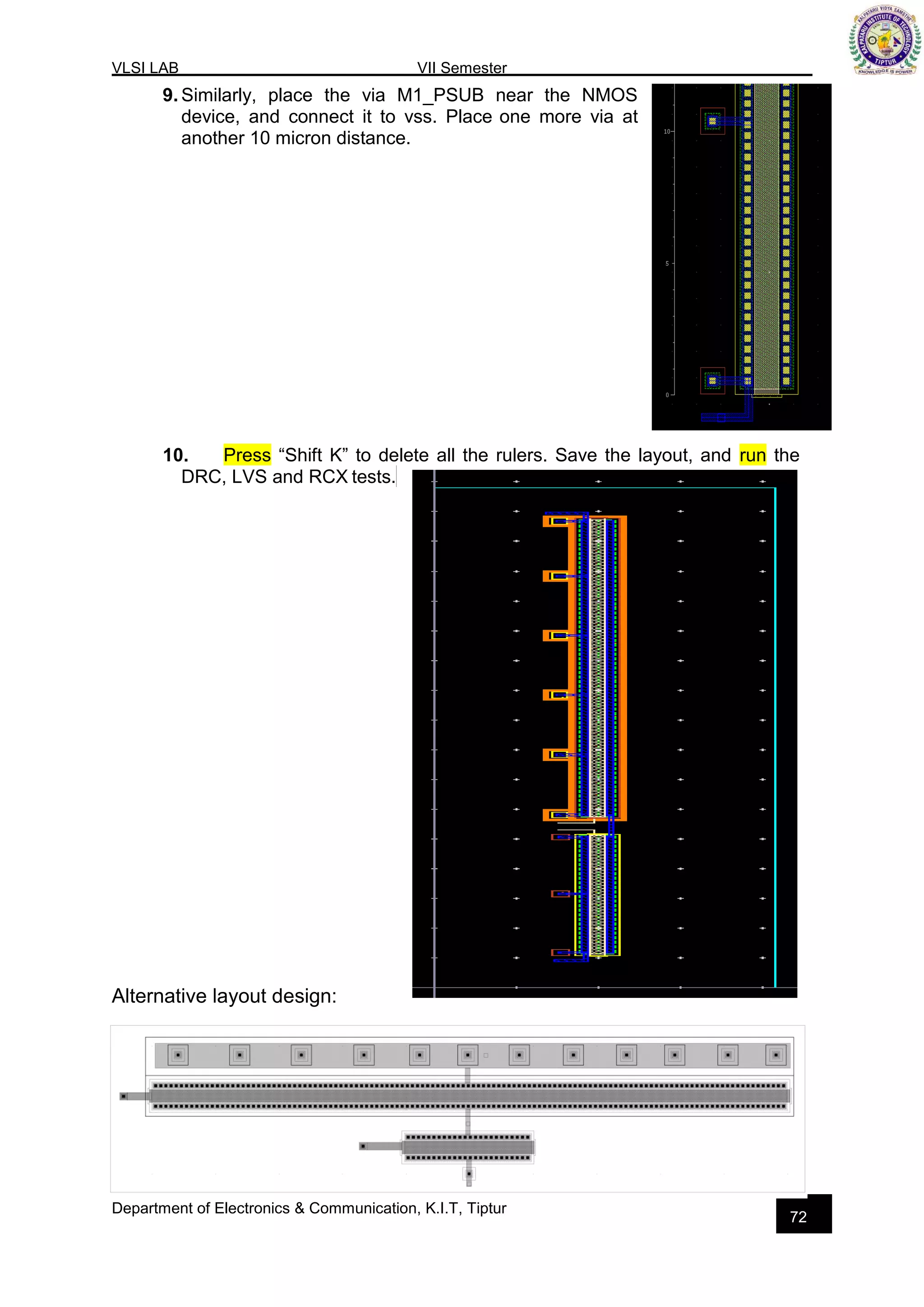
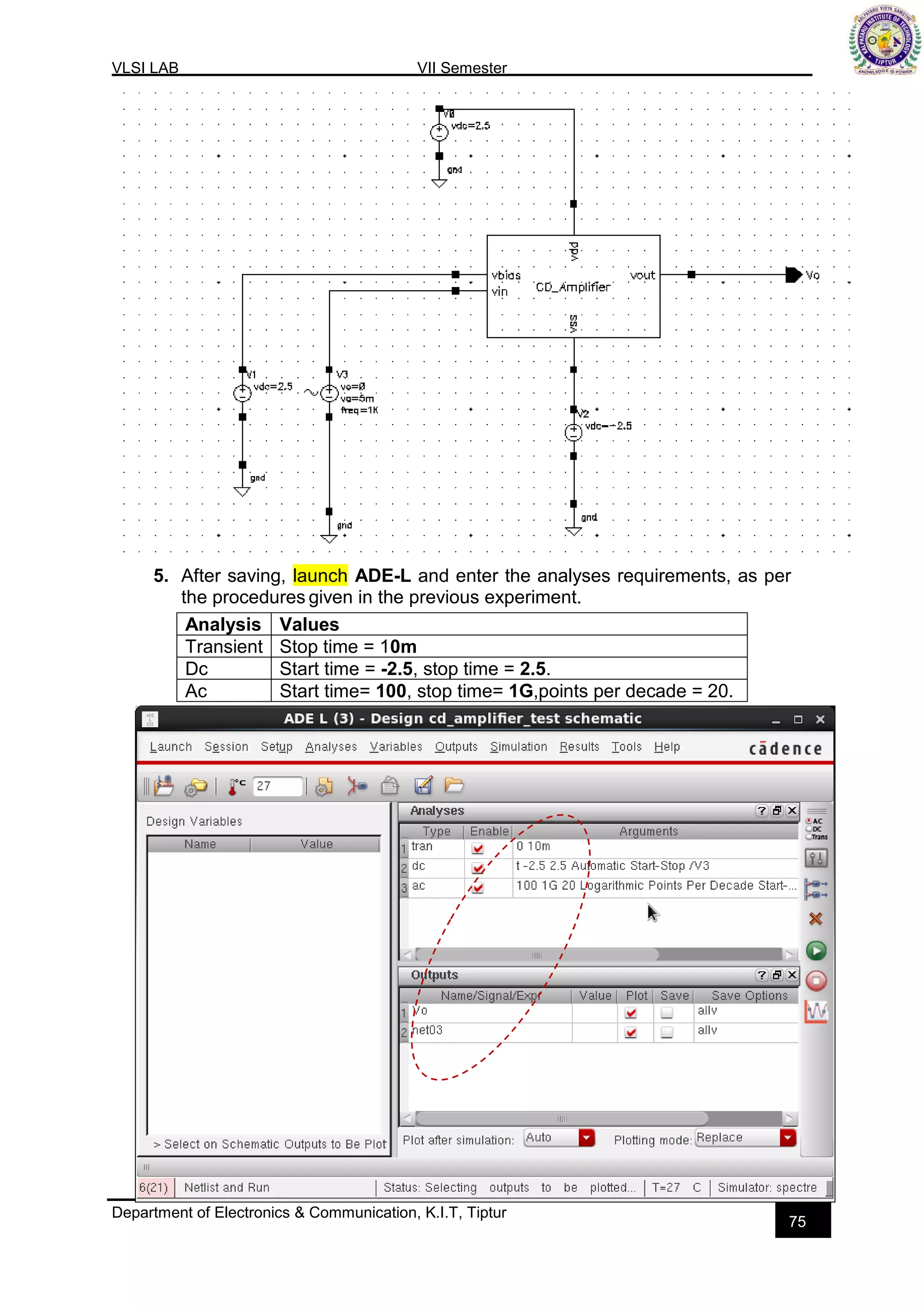
Analysis setup for common source and drain amplifiers, including wiring and layout procedures for design.
Reference books for VLSI design, layout, and simulation studies. Key information on design procedures.
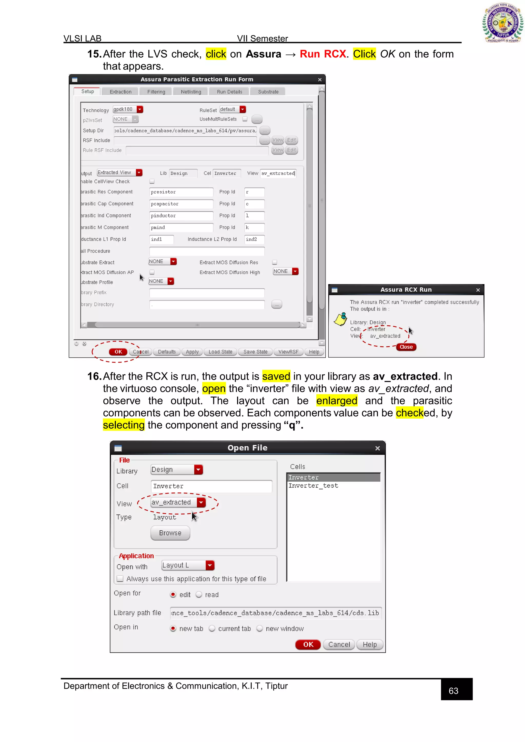
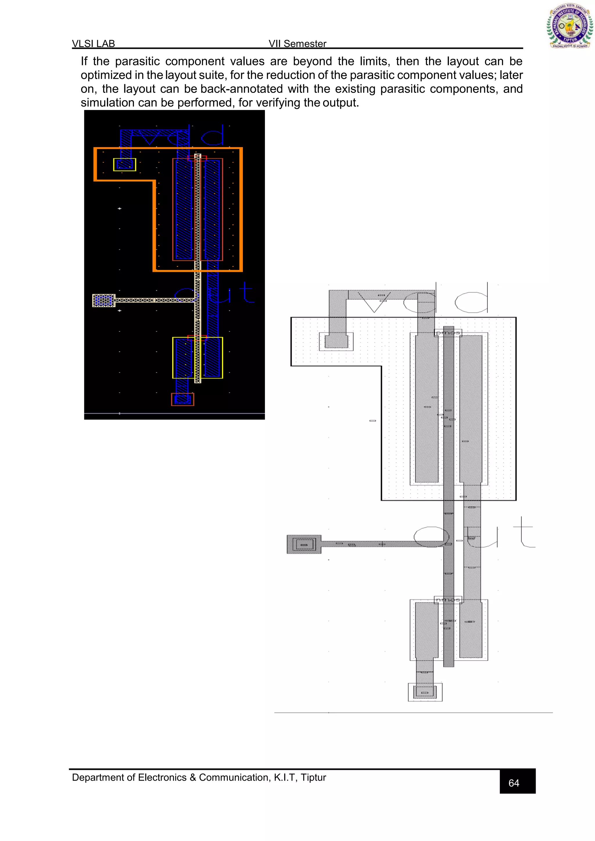
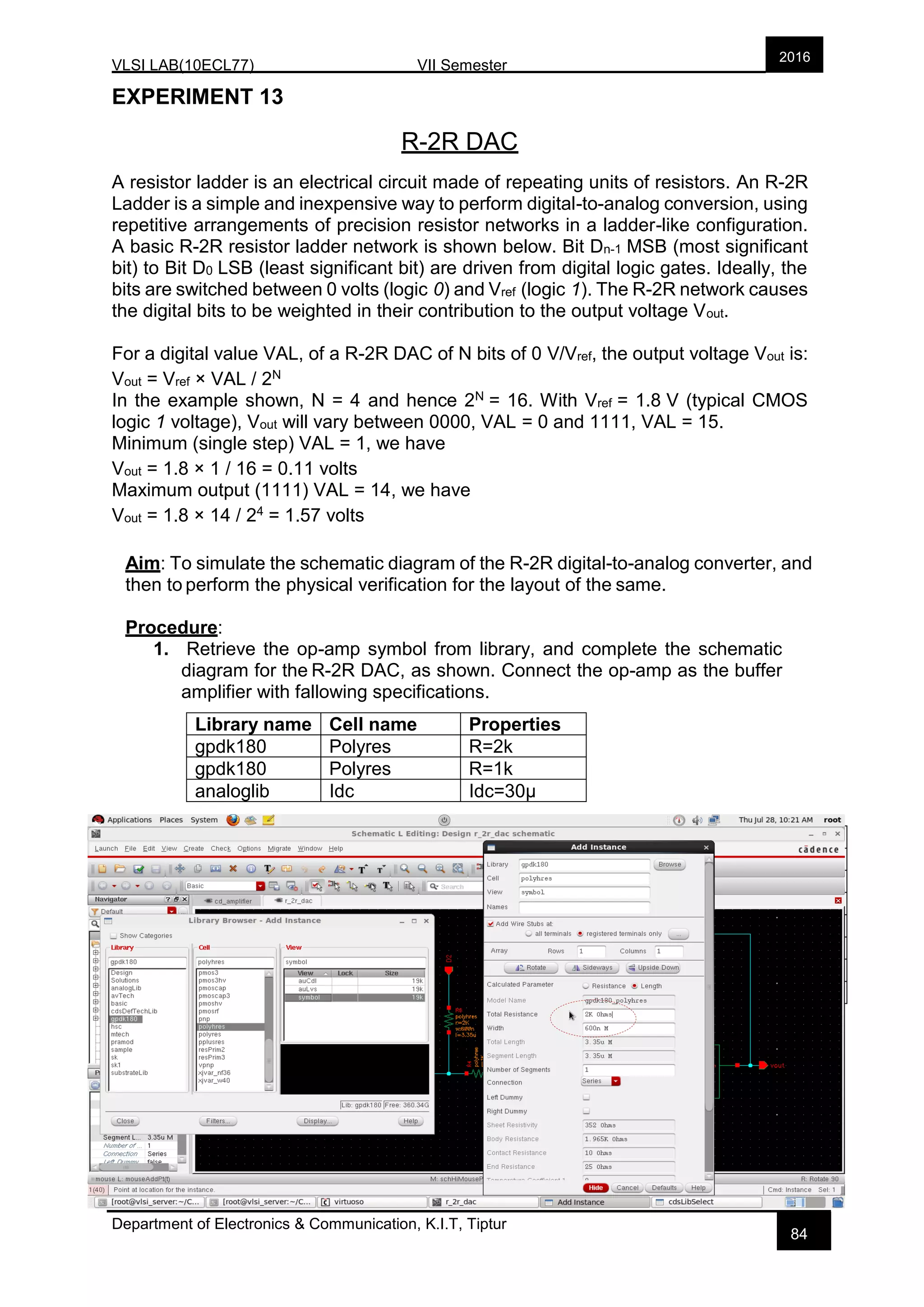
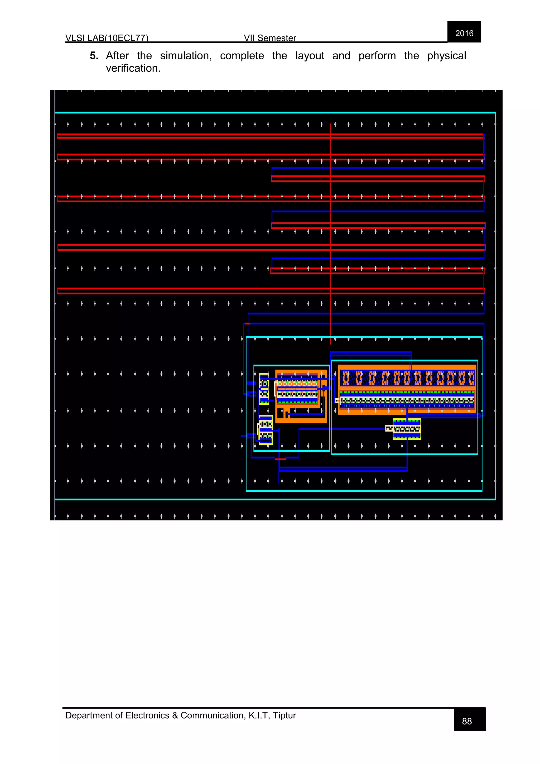
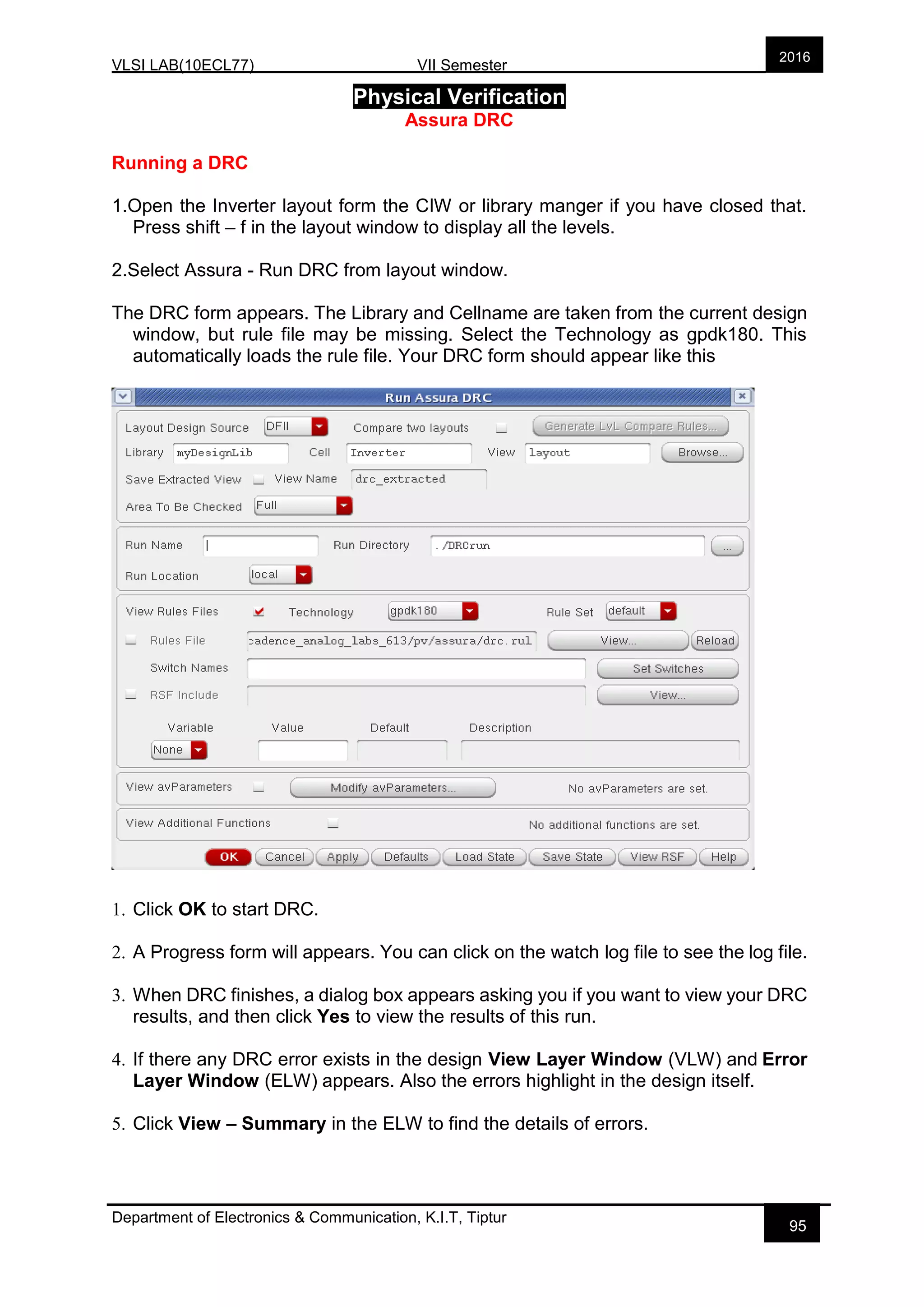
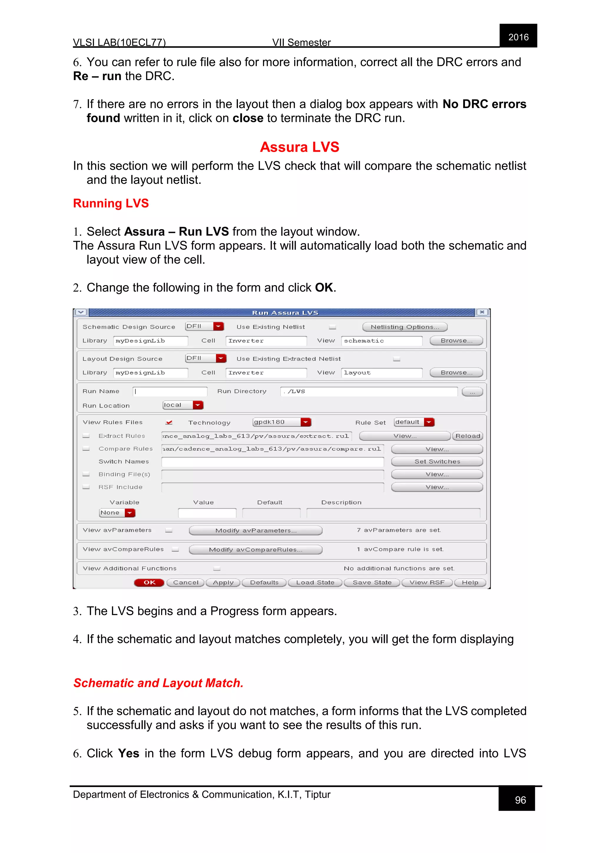
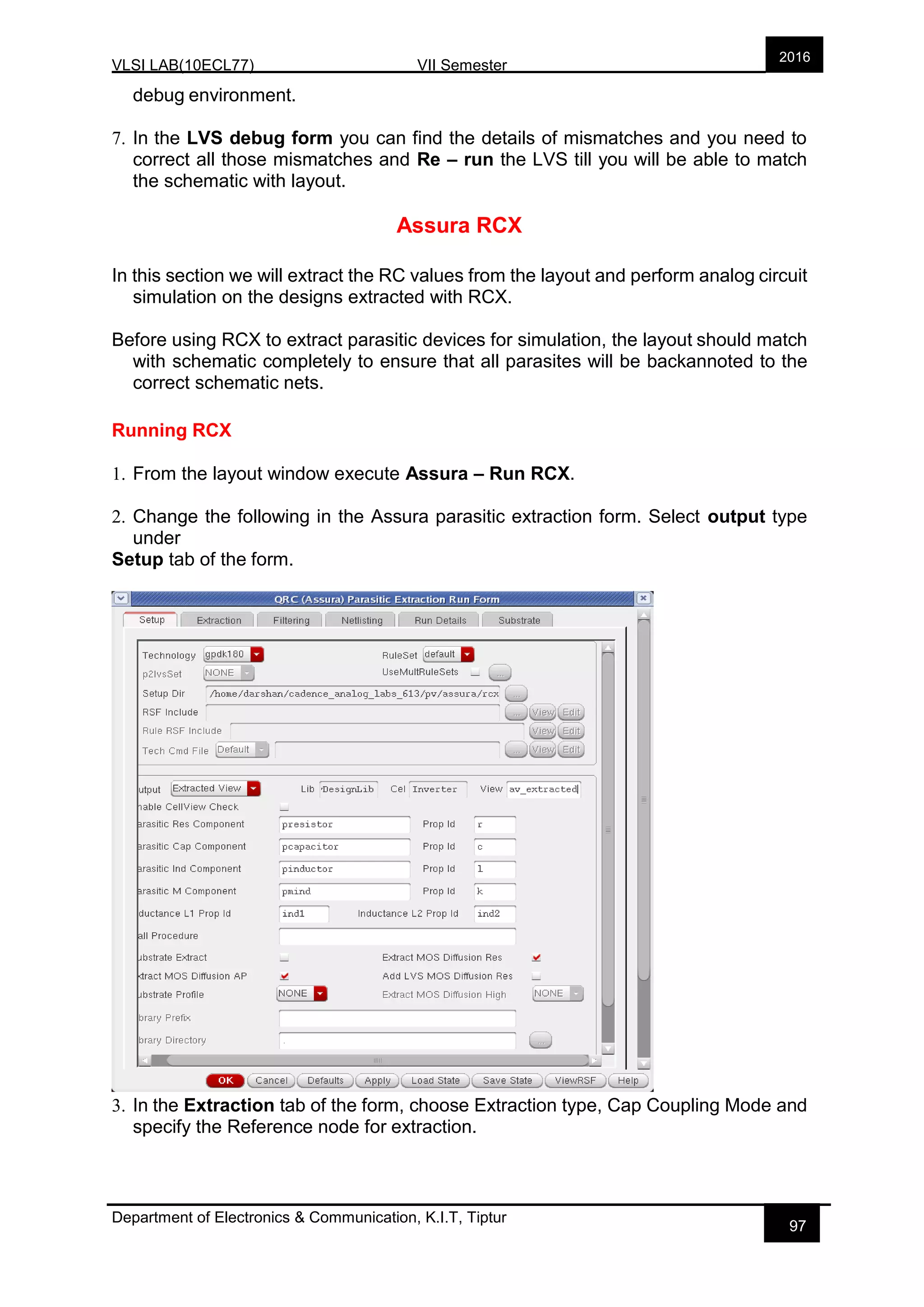
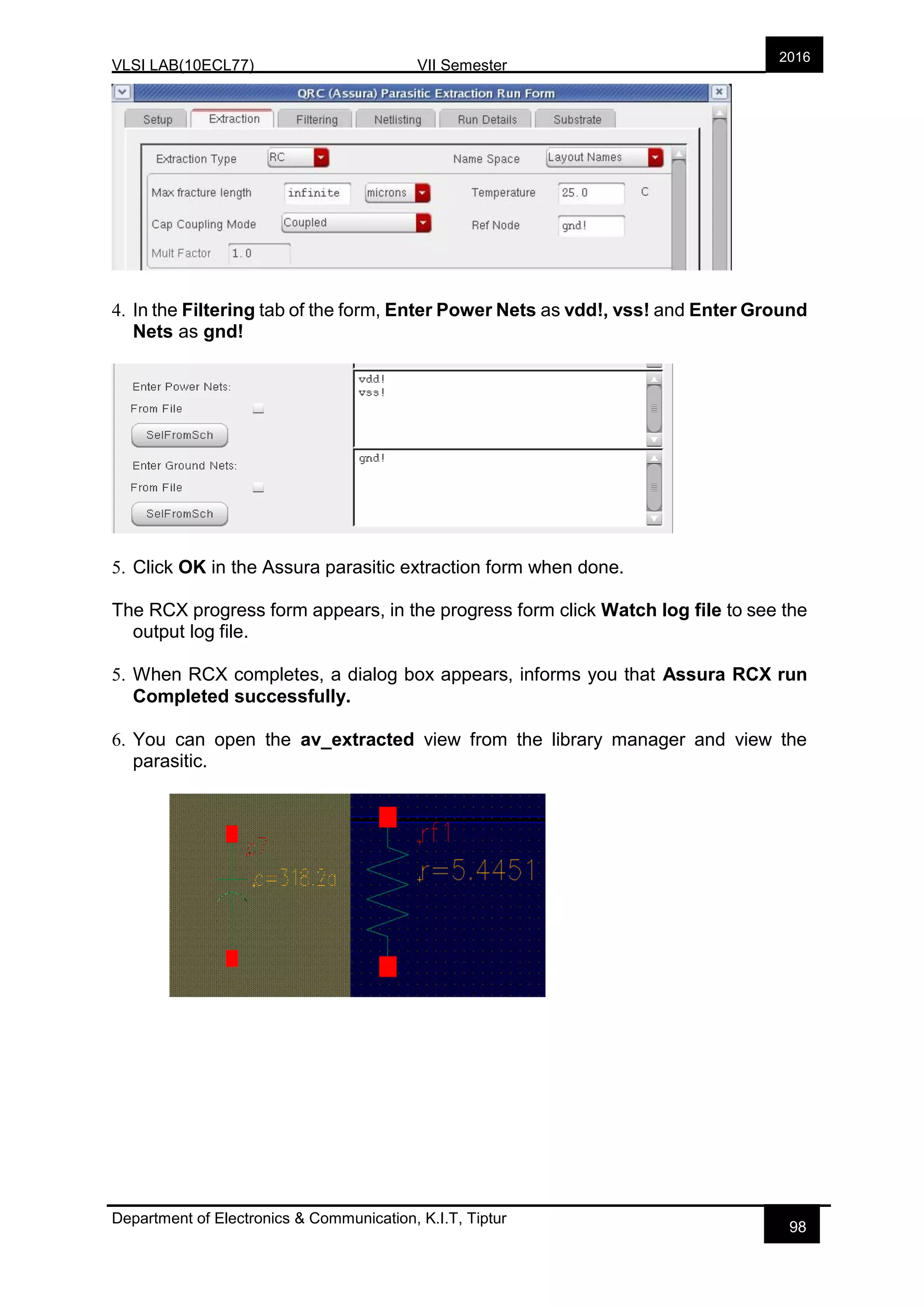
Detailed verification processes including DRC, LVS, and RCx to ensure layout corresponds with schematic.
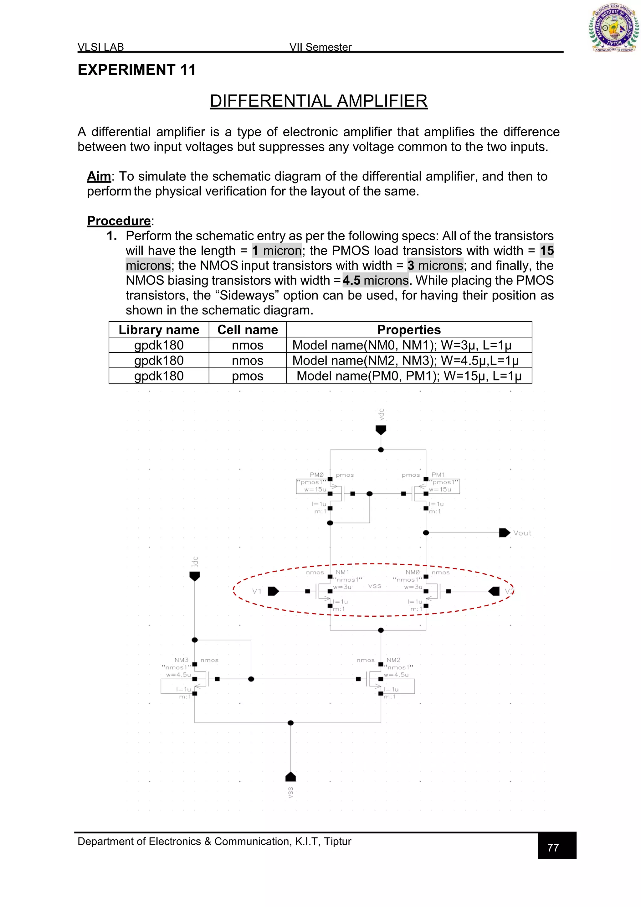
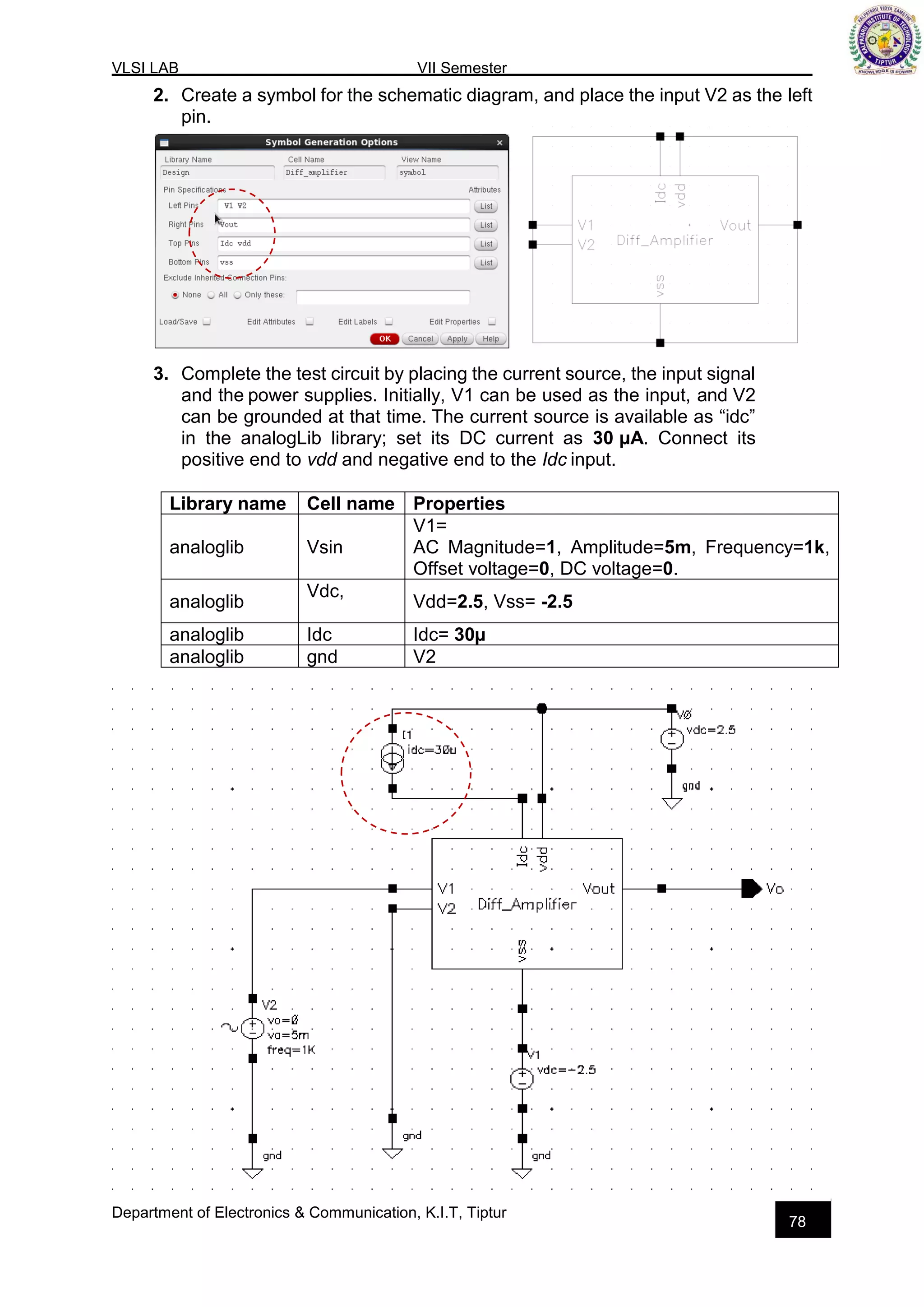
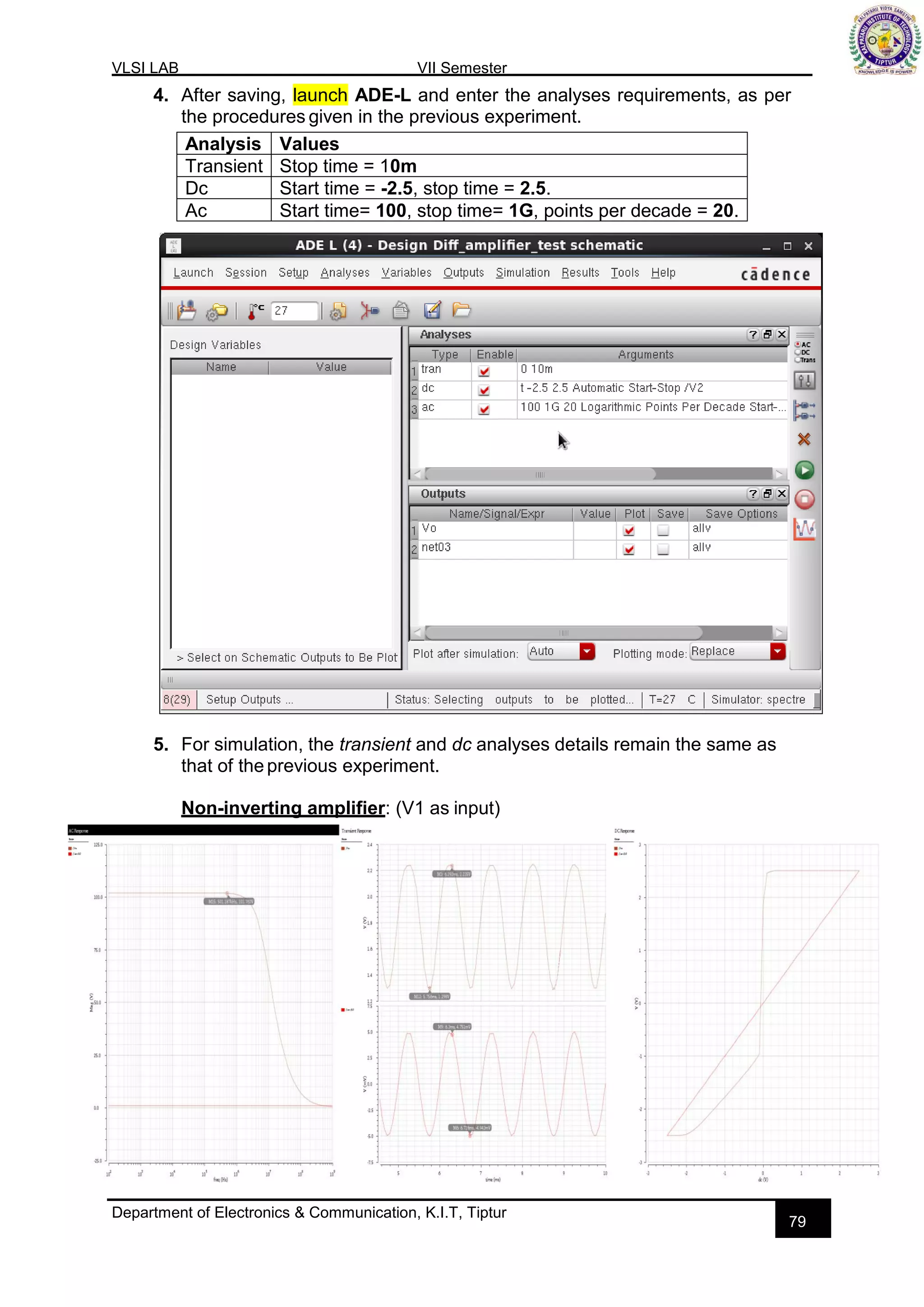
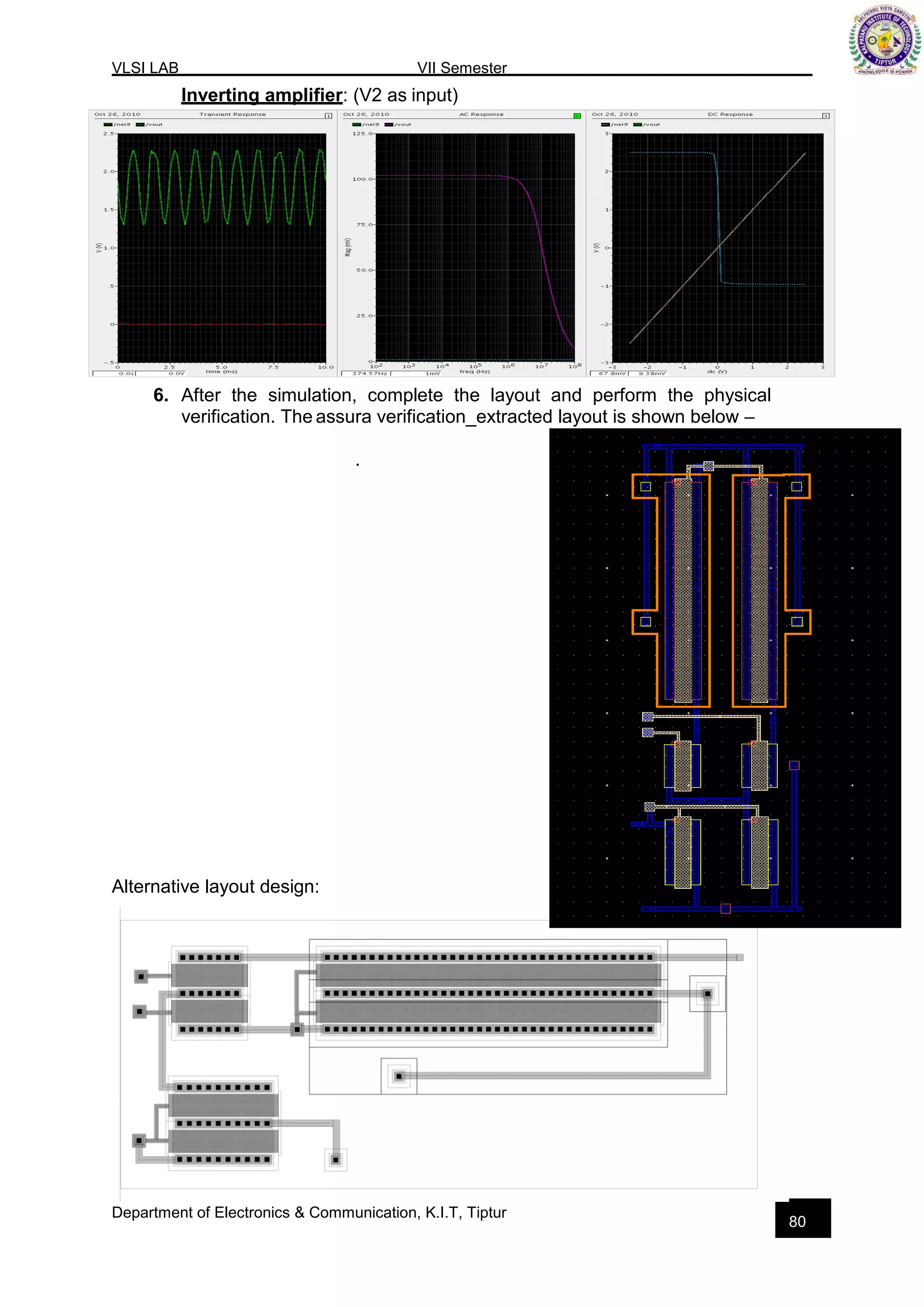
Overview of the differential amplifier, schematic design entry, completing the test circuit and verification.
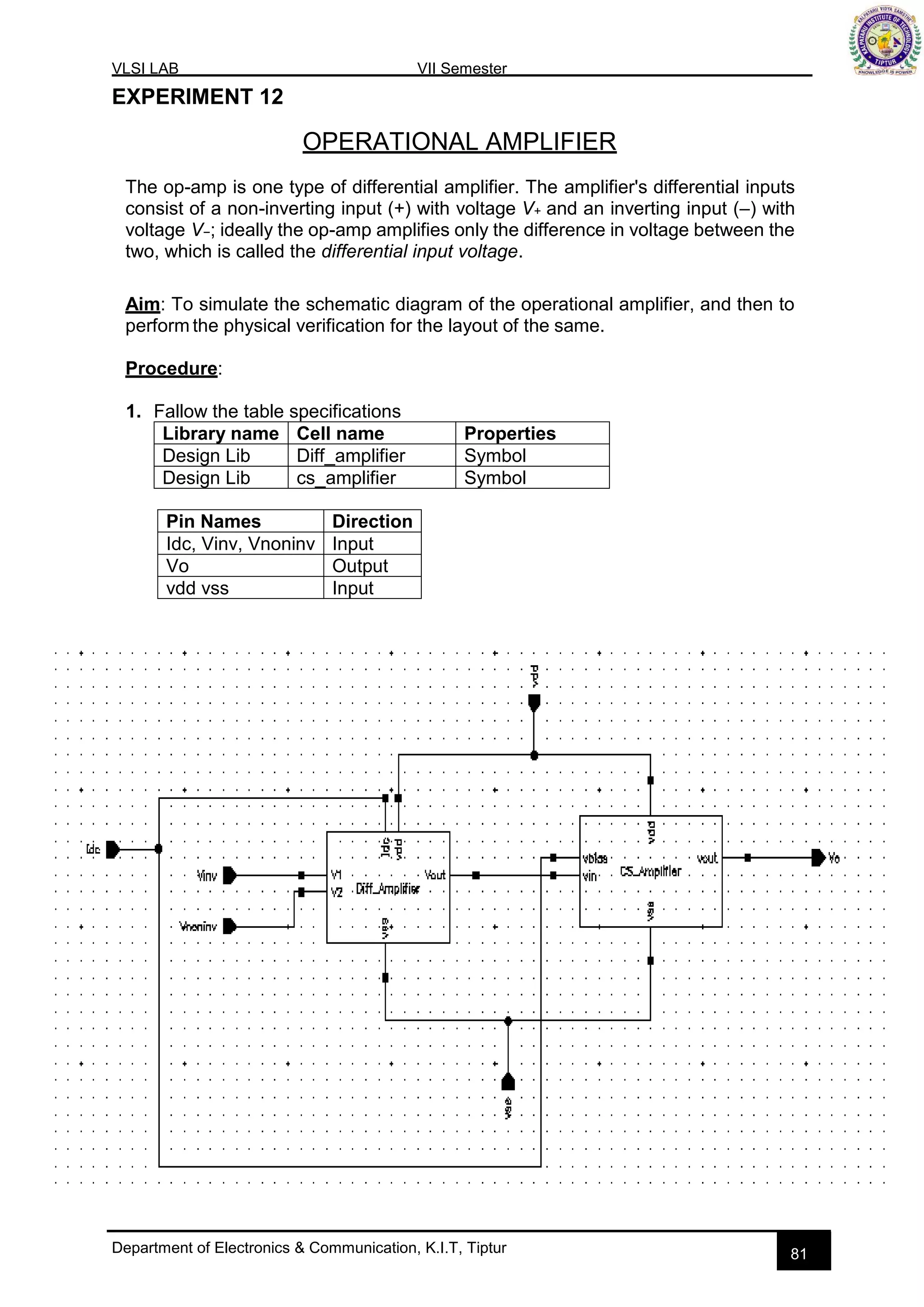
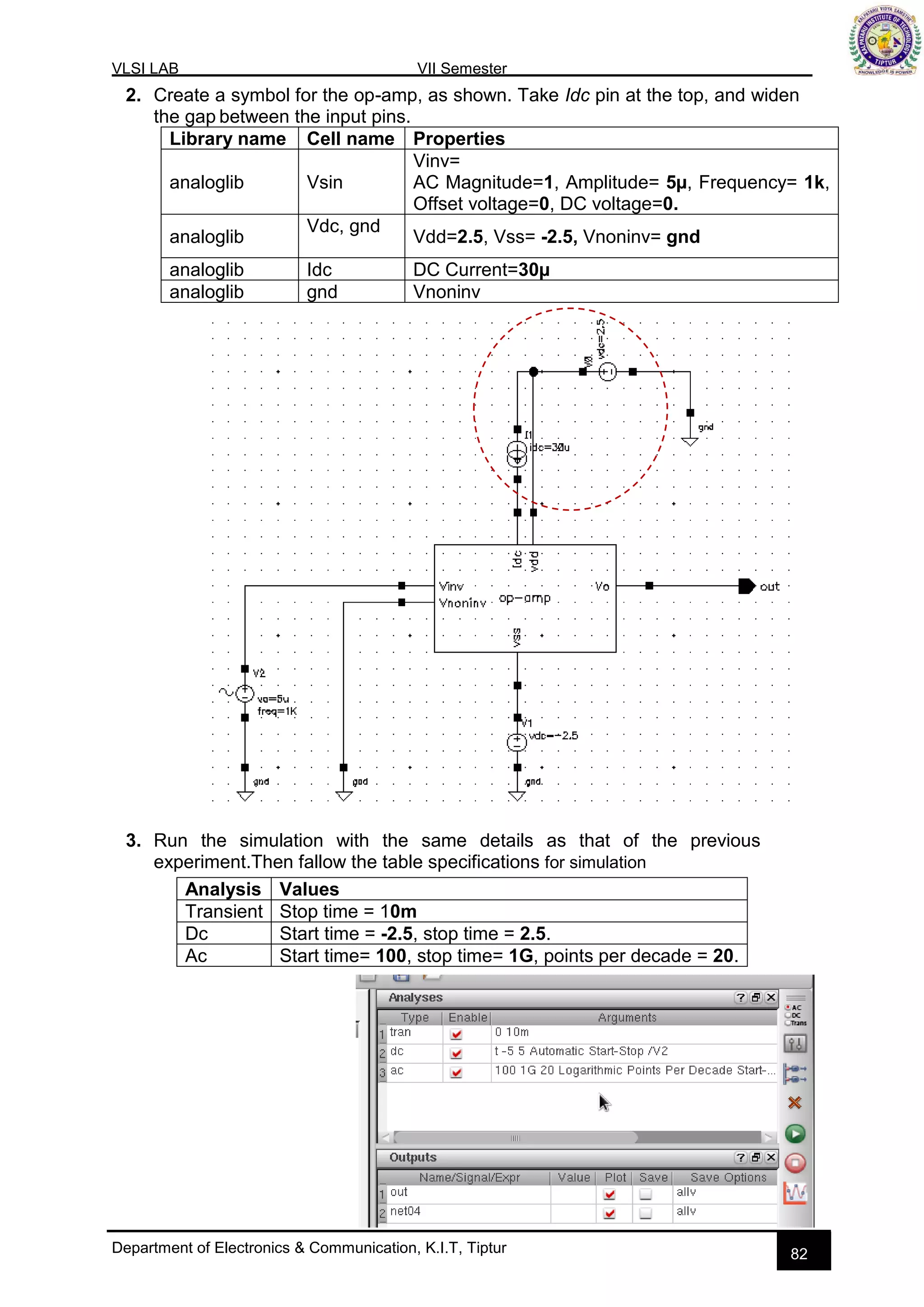
Procedure for creating operational amplifier design, simulation requirements, and layout verification process.
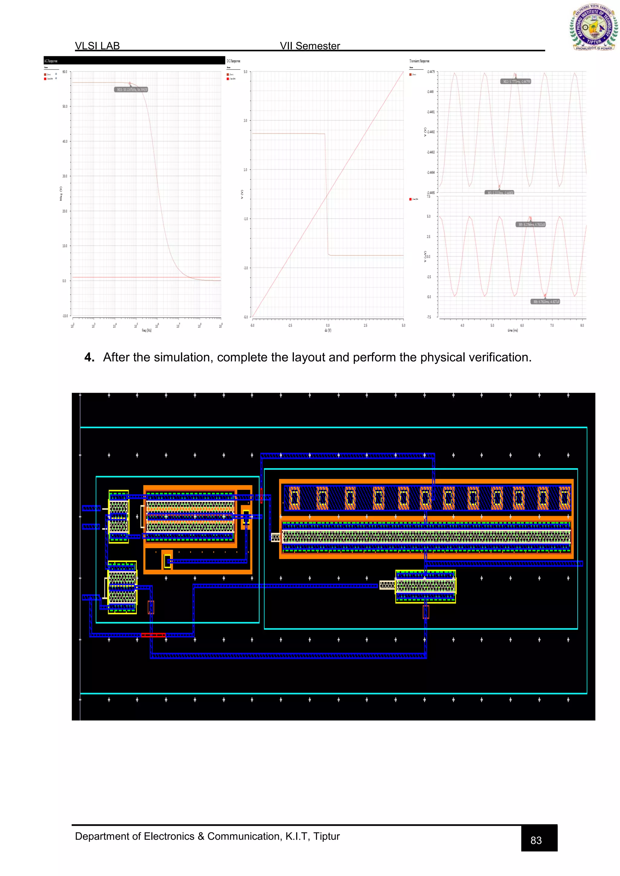
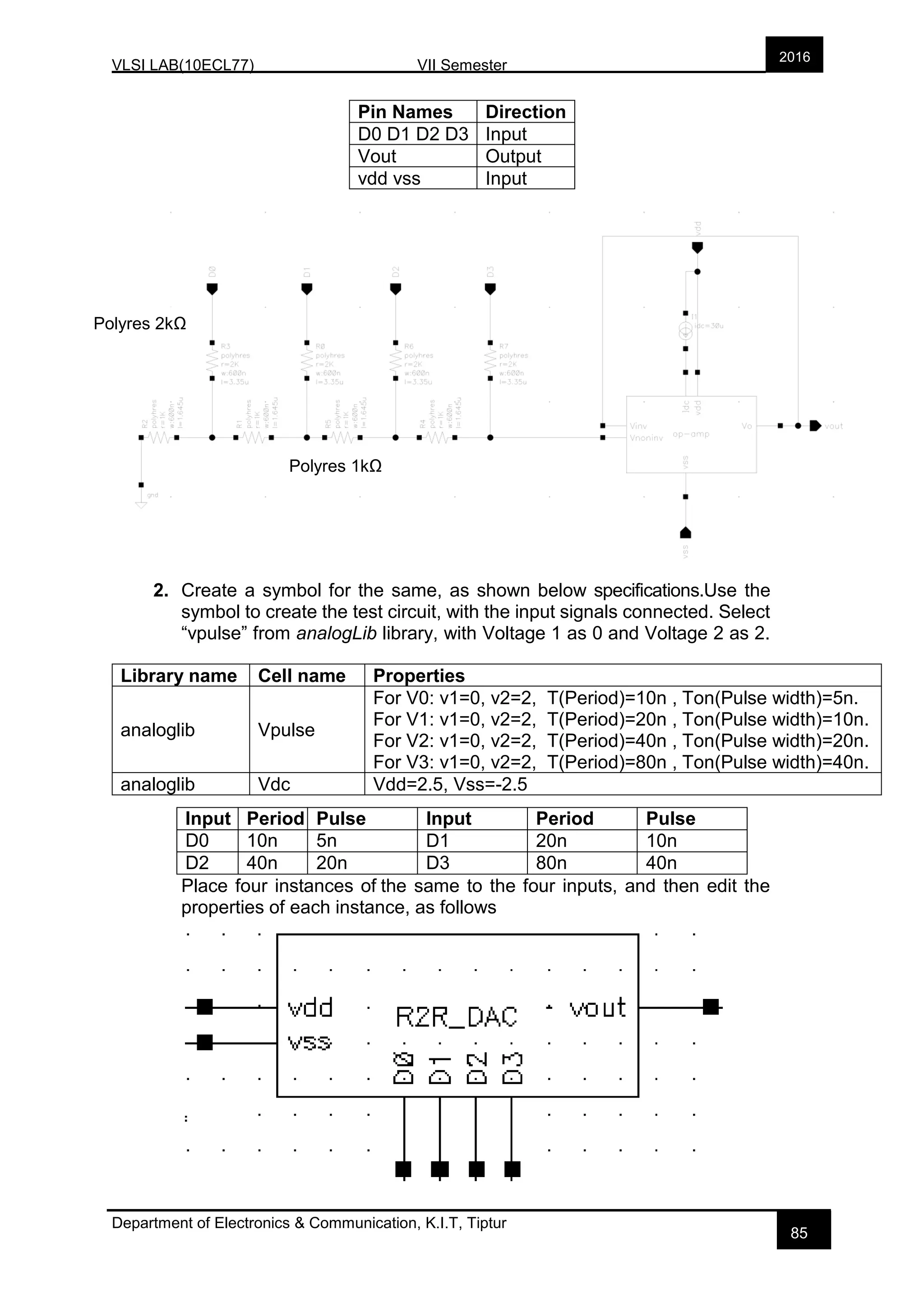
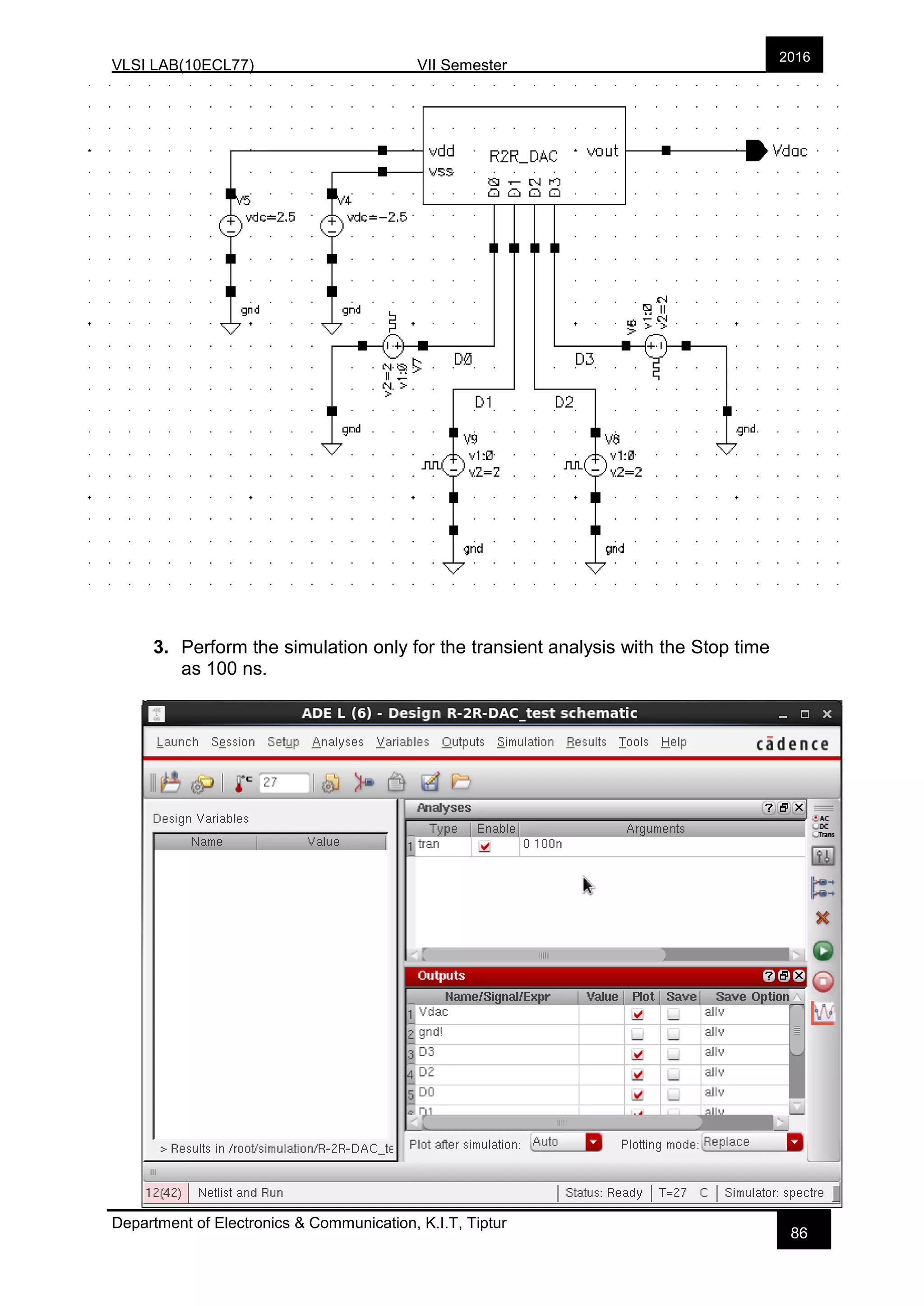
Basic concept of R-2R DAC, schematic creation, simulation for digital-to-analog conversion verification.
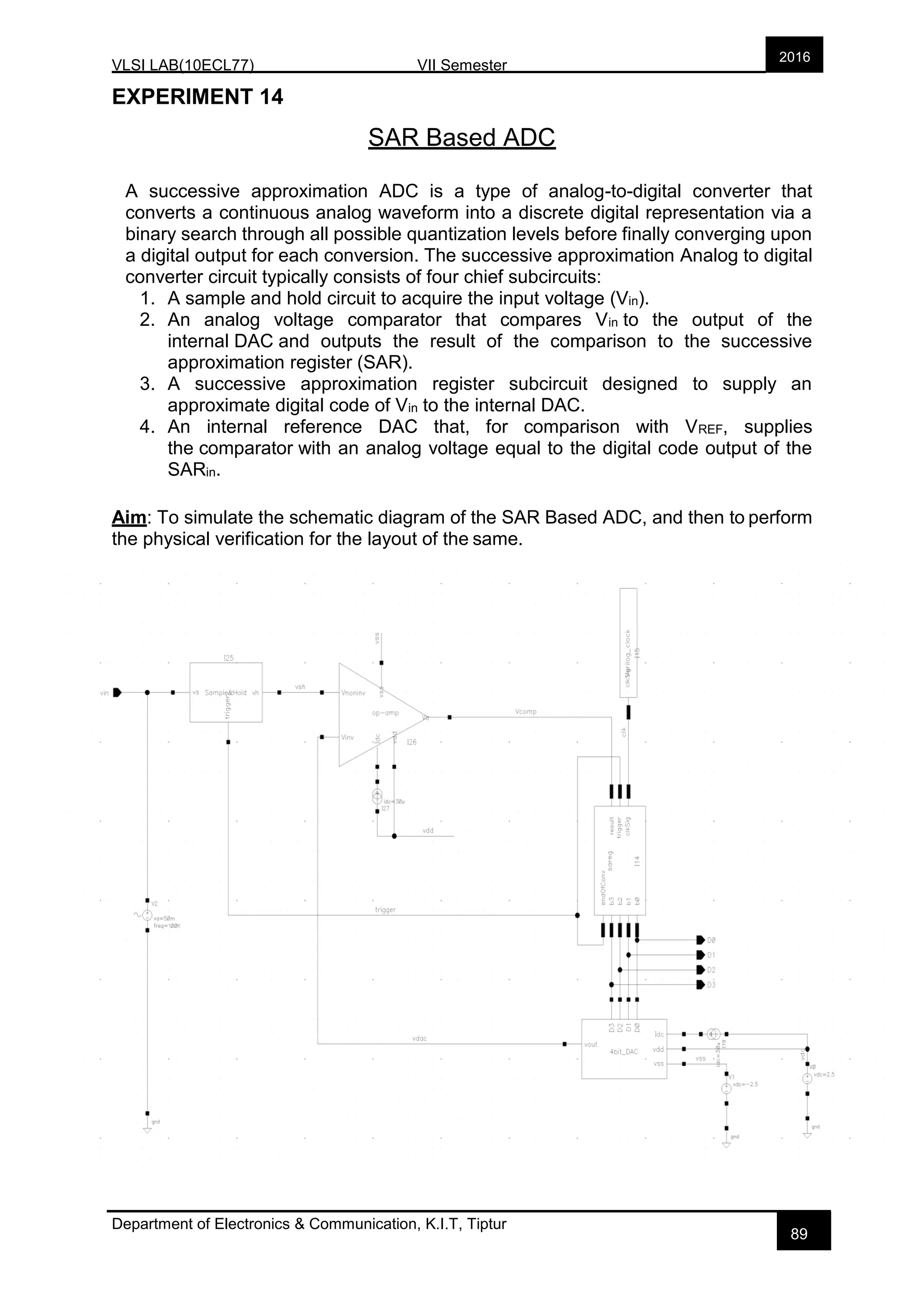
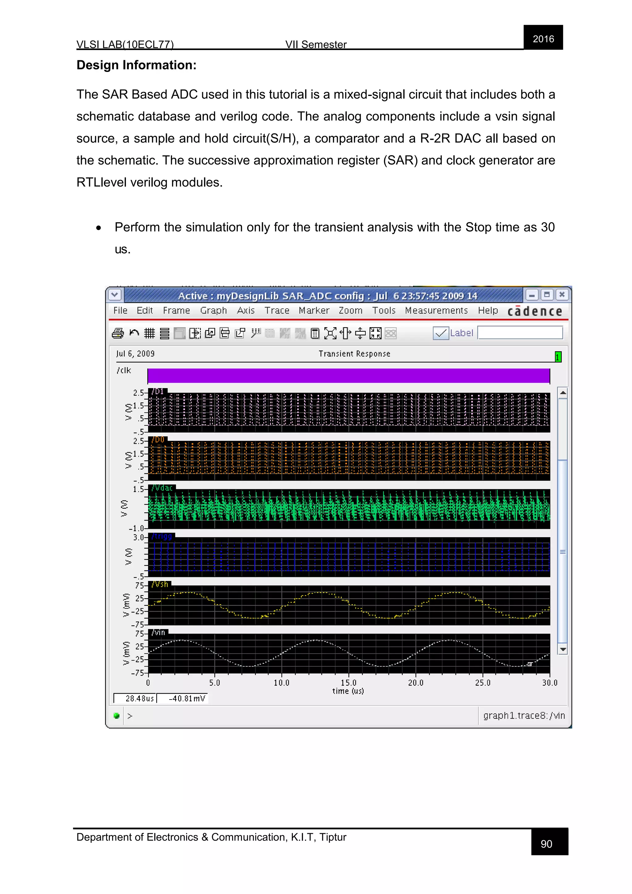
Overview of SAR ADC design, necessary components, simulation requirements, and circuit verification process.


