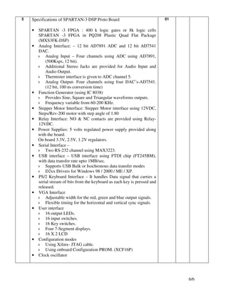
1. !" !# $ % &! '' ( )
' ' ) ' * * ) $ ( ) )
+ # '(
# , #- # # +
S. List of components/Equipments required Qty Rate Amount
No.
1 Xilinx Software – Lab License – 25 Users 5/10/25
• Xilinx Smart Compile technology providing a powerful MULTI
Users
design closure environment
• Support for the Virtex-5 family –The world's first 65nm
FPGA
• An integrated timing closure environment to help identify
bottlenecks in your Virtex-5 FPGA designs quickly and
easily.
• With a speed-grade or more in cost savings delivering the
lowest total cost in logic design
• Unparalleled ease-of-use and a wide range of supported
platforms
• Device Family Support
Spartan™-3A DSP, Spartan-3A, 3AN, Spartan-3, 3E,
Spartan-II, IIE, Coolrunner™-II, XPLA3, XC9500,
Virtex-5 LX, LXT, SXT, Virtex-4 FX, LX, SX, Virtex-II
Pro, Virtex-II, Virtex-E, Virtex
• Facility for design entry using HDL Editor (VHDL,
Verilog), Schematic Editor, FSM, CORE Generator.
• Has Synthesis Tool like Xilinx Synthesis Technology
(XST)
• Has ISE™ Foundation™ with the ISE™ Simulator
• Has PlanAhead™ Design and Analysis Tool.
• Has ChipScope™ Pro and the ChipScope™ Pro Serial
I/O Toolkit (In chip debugging tool).
• Has Implementation facility like, Floor planner,
Constraints Editor, Timing Driven place and Route,
Modular Design
• Has facility for programming all devices mentioned
above through the IMPACT interface.
• Has interface to Verification tool like Modelsim ( all
editions)
• Has facility to integrate with other tools like System
Generator/Accel DSP for DSP, Chip Scope Pro &
Embedded Development Kit.
1/6
2. 2 Active HDL – Software 5/10/
MULTI
Users
MICROWIND 3.5 or Latest CMOS Layout design & Simulation 5/10/25
Tool Multi
users
DSCH: Schematic Editor and Simulator
• User-friendly environment for rapid design of logic circuits
• Handles both conventional pattern-based logic simulation and
intuitive on-screen mouse-driven simulation
• Supports hierarchical logic design Built-in extractor which
generates a SPICE net list from the schematic diagram
(Compatible with PSPICE™ and Win Spice™)
• Current and power consumption analysis
• Generation of VERILOG description of the schematic for layout
generation & editing
• Facility for generation of user defined symbols for schematic
entry
• MOS level schematic support
• Immediate access to symbol properties (Delay, fan-out)
• Models and assembly support for 8051 and PIC 16F84
• Sub-micron, deep-submicron, nanoscale technology support
Supported by huge symbol library
NanoLambda Precision CMOS Layout tool upto 35 nanometers
• Sub-micron, deep-submicron, nanoscale technology support
• Unsurpassed illustration capabilities
• Design-error-free cell library (Contacts, vias, MOS devices, etc.)
• Advanced macro generator: capa, self, matrix, ROM, pads, path,
etc.)
• Incredible translator from logic expression into compact design-
error free layout
• Powerful automatic compiler from VERILOG circuit into layout
• On-line design rule checker: width, spacing, overlap, extension
rule verification
• Built-in extractor which generates a SPICE net list from layout
• Extraction of all MOS width and length
• Parasitic capacitance, crosstalk and resistance extracted for all
electrical nodes
• Import/Export CIF layout from 3rd party layout tools
• Up to 100,000 elementary boxes
• Lock & unlock layers to protect some part of the design from any
changes
• Enhanced editing commands and layout control
PRO thumb: Mixed Signal Simulation and Analysis
• Built-in SPICE-like analog simulator features fast time-domain,
2/6
3. voltage and current estimation, with very intuitive post
processing: frequency estimation, delay estimation. (No external
SPICE/ analog simulator.)
• Supports LEVEL1, LEVEL3 and BSIM4 models for all
technologies from 1.2µm down to 35nm
• MOS characteristic viewer, with access to main model parameter
• Real-case measurement data-base in 0.7,0.35, 0.25 and 0.18µm
for comparison with models
• The ability to label nodes allows intuitive control of the
simulation (Supply, clock, pulse, PWL, sinus, maths)
• Time-domain voltage and current waveforms available at the
press of one single icon
• DC/AC characteristics, signal frequency vs. time, eye diagrams
• Min/Type/Max analog simulation
• Convenient Monte-carlo simulation
• Powerful fast-Fourier Transform to support radio-frequency
circuit simulation
• On screen Power estimation
• Sophisticated parametric simulation to investigate the effect of
several key parameters on the circuit performances: R, L, C,
temperature, supply voltage, etc.
• Huge device simulation model library
• Inbuilt interconnect analyzer to compute field between ground
planes and conductor
PROtutor: Specially Enabled University Edition with Enhanced
Training Features
• A valuable tutor to understand the MOS characteristics, with a
user interface that beginners will like
• Change the model parameters and see their effects on Id/Vd,
Id/Vg Id(log)/Vg, threshold vs Length
• You can also fit the simulations with measurements we made in
test-chips fabricated in 0.35, 0.25 and 0.18 µm
• Full length tutorial on MOS models is provided in manual, with
details on all parameters
• Supports 1,3 and BSIM4 MOS models
• 200-pages documentation including several aspects of logic
design
• More than 150 basic circuits ready to simulate
VirtuosoFab: Touch the Deep-Sub Micron Technology
• 3D fabrication process simulator with cross sectional viewer
• Step-by-step 3-D visualization of fabrication for any portion of
layout
• See how the contacts and metallization are created
3/6
4. • See the self-aligned diffusion after the polysilicon gate is
fabricated
• Check planes of VDD, VSS, and others signals
• Check the oxide structure, the low dielectric (Low K) and high K
(SiO2) sandwich, and passivation
• User can check the gate oxide and the MOS lateral drain
diffusion structure
MEMsim:Non Volatile Floating Gate Memory Simulator
• Simulation of non-volatile memories such as EPROM, EEPROM
and FLASH using double-gate MOS
• Erasure of floating gates and removal all electrons.
• Programming can be performed by a very high voltage supply on
the gate
3 CPLD Protoboard 01
Features
• CPLD – Compatibility -
Xilinx CPLD XC9572 / XC95108 in PLCC 84 package.
• User IOs –
16 Digital I/Ps and O/Ps with LED indication.
• User interface
16 output LEDs.
16 input switches.
2x2 Key matrix.
4 7-Segment displays.
• Configuration modes
Using Xilinx- JTAG cable.
• Clock oscillator
Standard Accessories
• User Manual.
• Lab Manual covering all Experiments as per RTU Syllabus.
• Power Supply.
• Download Cable.
• Sample Design.
4 Specification of SPARTAN-3 Protoboard 01
Features
• FPGA – Compatibility
Xilinx Spartan-3 XC3S400 in PQ208 pin package.
• Configuration through
Flash PROM.( Optional)
JTAG Port.
• Power Supply
Vccio and Vccint are generated on board using regulators.
4/6
5. • User Interface
16 Digital Output LEDs
4 X 4 Matrix Keyboard
Six 7 Segment Display
• Clock oscillator
• User I/Os
Maximum 79 I/Os.
• Standard Configuration
FPGA – XC3S400.
• Standard Accessories
User Manual.
Lab Manual covering all Experiments as per RTU Syllabus.
Codes for Demonstration.
Download Cable.
Power Supply Adapter.
One RS-232 channel using MAX3223
• Interface Module
Traffic Light Controller
Real Time Clock Circuit
ADC- DAC
• RS232 Serial Interface
RS232C compatible connectivity is provided using device
MAX3223. Signals provided are Rx, Tx RTS and CTS.
These signals are terminated on 9-pin D connector
• Analog Interface: – 12 bit AD7891 ADC and 12 bit AD7541
DAC.
Analog Input – Eight channels using ADC using AD7891,
(500Ksps, 12 bit).
Analog Output- Two channels using Two DAC’s-AD7541.
(12 bit, 100 ns conversion time)
• Downloading Cable and Connector
For downloading the design from PC, one 10-pin FRC connector is
provided on board.
(JTAG)
• Configuration
Board supports two different configuration modes
Master Serial Mode (Configuration PROM.)
Boundary Scan Mode.(JTAG)
Configuration modes can be selected by setting mode pins using on
board jumpers.
• Boundary Scan Mode
In this mode, FPGA and / or PROM can be configured through
JTAG port.
5/6
6. 5 Specifications of SPARTAN-3 DSP Proto Board 01
• SPARTAN -3 FPGA : 400 k logic gates or 8k logic cells
SPARTAN -3 FPGA in PQ208 Plastic Quad Flat Package
(MXS3FK-DSP)
• Analog Interface: – 12 bit AD7891 ADC and 12 bit AD7541
DAC.
Analog Input – Four channels using ADC using AD7891,
(500Ksps, 12 bit).
Additional Stereo Jacks are provided for Audio Input and
Audio Output.
Thermister interface is given to ADC channel 5.
Analog Output- Four channels using four DAC’s-AD7541.
(12 bit, 100 ns conversion time)
• Function Generator (using IC 8038)
Provides Sine, Square and Triangular waveforms outputs.
Frequency variable from 60-200 KHz.
• Stepper Motor Interface: Stepper Motor interface using 12VDC,
Steps/Rev-200 motor with step angle of 1.80
• Relay Interface: NO & NC contacts are provided using Relay-
12VDC.
• Power Supplies: 5 volts regulated power supply provided along
with the board.
On board 3.3V, 2.5V, 1.2V regulators.
• Serial Interface –
Two RS-232 channel using MAX3223.
• USB interface – USB interface using FTDI chip (FT245BM),
with data transfer rate upto 1MB/sec.
Supports USB Bulk or Isochronous data transfer modes
D2xx Drivers for Windows 98 / 2000 / ME / XP.
• PS/2 Keyboard Interface – It handles Data signal that carries a
serial stream of bits from the keyboard as each key is pressed and
released.
• VGA Interface
Adjustable width for the red, green and blue output signals.
Flexible timing for the horizontal and vertical sync signals.
• User interface
16 output LEDs.
16 input switches.
16 Key switches.
Four 7-Segment displays.
16 X 2 LCD
• Configuration modes
Using Xilinx- JTAG cable.
Using onboard Configuration PROM. (XCF16P)
• Clock oscillator
6/6