Bapuji Educational Association®
BapujiInstitute of Engineering and Technology Davangere - 577004
Department of Electronics & Communication Engineering
Internship Progreess Presentation
On
VLSI Design and Verification
By
NANDITHA D
(4BD22EC412)
Mrs. POORNIMA G N Dr. G. S. SUNITHA
M Tech, Ph D., MISTE M. Tech(DEAC),Ph.D., MISTE,FIETE,FIE
INTERNSHIP GUIDE PROGRAM COORDINATOR
2.
Vision of theDepartment
To be in the forefront in providing quality technical education and research in Electronics &
Communication Engineering to produce skilled professionals to cater to the challenges of the
society.
Mission of theDepartment
M1: To facilitate the students with profound technical knowledge through effective teaching learning
process for a successful career.
M2:To impart quality education to strengthen students to meet the industry standards and face
confidently the challenges in the programme.
M3:To develop the essence of innovation and research among students and faculty by
providing infrastructure and a conducive environment.
M4:To inculcate the student community with ethical values, communication skills, leadership
qualities, entrepreneurial skills and lifelong learning to meet the societal needs.
3.
COURSE LEARNING OBJECTIVES
Thiscourse will enable us to:
1. Experience a real-life engineering workplace and understand how their engineering
knowledge and skills can be utilized in Industry.
2. Expose to the current Technological trends relevant to the field of training.
3. To enhance communication skills, teamwork capabilities and develop professional
behaviour.
4. Use Internship experience to develop their engineering skills and practices that
boost
their employability.
5. Gain experience in writing technical/projects reports and expose students to the
engineer’s responsibilities and ethics.
4.
Contents
1.Work Carried OutIn First Month
• Fundamentals Of VLSI Design And Verilog Basics
• VLSI:Syntax, Sematics, And Core Representation
• Gate level modelling and Concept Wire
2.Work Carried Out In Second Month
• Continuos Assignments and Data Operators
• Verilog Operators
• Procedural Blocks and Assignments in Verilog
3.Work Carried Out Third Month
• Introduction to SystemVerilog And Verification
• Enumerated Type Access Methods
• Arrays and Queues
5.
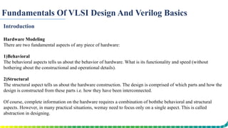
Fundamentals Of VLSIDesign And Verilog Basics
Introduction
Hardware Modeling
There are two fundamental aspects of any piece of hardware:
1)Behavioral
The behavioral aspects tells us about the behavior of hardware. What is its functionality and speed (without
bothering about the constructional and operational details).
2)Structural
The structural aspect tells us about the hardware construction. The design is comprised of which parts and how the
design is constructed from these parts i.e. how they have been interconnected.
Of course, complete information on the hardware requires a combination of boththe behavioral and structural
aspects. However, in many practical situations, wemay need to focus only on a single aspect. This is called
abstraction in designing.
6.
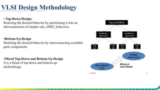
VLSI Design Methodology
▪Top-Down Design:
Realizing the desired behavior by partitioning it into an
interconnection of simpler sub_x0002_behaviors.
▪Bottom-Up Design
Realizing the desired behavior by interconnecting available
parts components.
▪Mixed Top-Down and Bottom-Up Design
It is a blend of top-down and bottom-up
methodology.
7.
Modeling Styles
Verilog isboth, behavioral and structural language. Designs in Verilog can be described at all the four
levels of abstraction depending on needs of design.
Behavioral Level: -
Used to model behavior of design without concern for the hardware implementation details. Designing at
this level is very similar to C programming.
Dataflow Level [RTL]: -
Module is specified by specifying the data flow. The designer is aware of how the data flows between
registers.
Gate Level: -
Module is implemented in terms of logic gates & interconnections between them. Design at this level is
similar to describing design in terms of gate level logical diagram.
Switch Level: -
lowest level of abstraction provided by Verilog. Module can be implemented in terms of switches, storage
nodes & interconnection between them.
8.
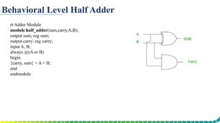
Behavioral Level HalfAdder
// Adder Module
module half_adder(sum,carry,A,B);
output sum; reg sum;
output carry; reg carry;
input A, B;
always @(A or B)
begin
{carry, sum} = A + B;
end
endmodule
9.
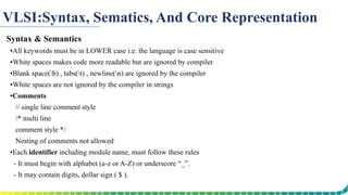
VLSI:Syntax, Sematics, AndCore Representation
Syntax & Semantics
▪All keywords must be in LOWER case i.e. the language is case sensitive
▪White spaces makes code more readable but are ignored by compiler
▪Blank space(b) , tabs(t) , newline(n) are ignored by the compiler
▪White spaces are not ignored by the compiler in strings
▪Comments
// single line comment style
/* multi line
comment style */
Nesting of comments not allowed
▪Each identifier including module name, must follow these rules
- It must begin with alphabet (a-z or A-Z) or underscore “_”.
- It may contain digits, dollar sign ( $ ).
- No space is allowed inside an identifier.
10.
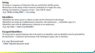
String
▪A string isa sequence of characters that are enclosed by double quotes.
▪Restriction on the string is that it must be contained on a single line only.
▪Strings are treated as a sequence of one – byte ASCII values.
E.g. “Hello Verilog HDL” // is a string
Identifiers
▪Identifiers are names given to objects so that can be referenced in the design.
▪Identifiers are made up of alphanumeric characters, the underscore( _ ) and dollar sign ( $ ).
▪Identifiers start with an alphanumeric character or an underscore.
E.g. reg value // value is an identifier
Escaped Identifiers
▪If a keyword or special character has to be used in an identifier, such an identifier must be preceded by
the backslash ( ) character and terminate with whitespace (space, tab, or newline)
E.g. reg //Keyword used
valid! //Special character used
11.
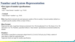
Number and SystemRepresentation
▪Two types of number specifications:
- Sized
<size>’<base format><number> e.g. 3’b101
- Unsized
’<base format><number> e.g. ’b101
▪Size: Specified in decimal only and represents number of bits in number. Unsized numbers default to a
compiler specific number of bits ( at least 32 bits ).
▪Base Format:
Represent the radix. Legal base formats are decimal (‘d or ‘D), hexadecimal (‘h or ‘H), binary (‘b or ‘B)
and octal (‘o or ‘O). Numbers, specified without a <base format> specification are decimal numbers by
default.
▪Number:
The number is specified as consecutive digits from 0,1,2,3,4,5,6,7,8,9,a,b,c,d,e,f. Only a subset of
these digits is legal for a particular base.
Uppercase letters are legal for number specification.
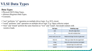
VLSI Data Types
DataTypes
▪ Physical (NET) Data Types.
▪ Abstract (Register) Data Types.
▪ Constants.
▪ “wor” performs “or” operation on multiple driver logic. E.g. ECL circuit
▪ “wand” performs “and” operation on multiple driver logic. E.g. Open collector output
▪ “trior” and “triand” perform the same function as “wor” and “wand”, but model outputs with
resistive loads.
14.
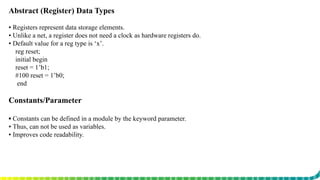
Abstract (Register) DataTypes
▪ Registers represent data storage elements.
▪ Unlike a net, a register does not need a clock as hardware registers do.
▪ Default value for a reg type is ‘x’.
reg reset;
initial begin
reset = 1’b1;
#100 reset = 1’b0;
end
Constants/Parameter
▪ Constants can be defined in a module by the keyword parameter.
▪ Thus, can not be used as variables.
▪ Improves code readability.
15.
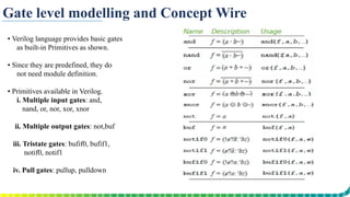
Gate level modellingand Concept Wire
▪ Verilog language provides basic gates
as built-in Primitives as shown.
▪ Since they are predefined, they do
not need module definition.
▪ Primitives available in Verilog.
i. Multiple input gates: and,
nand, or, nor, xor, xnor
ii. Multiple output gates: not,buf
iii. Tristate gates: bufif0, bufif1,
notif0, notif1
iv. Pull gates: pullup, pulldown
16.
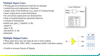
Multiple Input Gates
▪Writing gate level hardware model for an and-gate
▪ module keyword implements a hardware
▪ unique name of the hardware (e.g. name of a human being)
▪ input, output ports or pins declarations
▪ by convention output ports are declared first
▪ body of module/hardware represents behavior
▪ concept of instantiation
module and_gate_2_input(O, A, B);
output O;
input A, B;
and and1(O, A, B);
endmodule
Multiple Output Gates
▪ These gates have only one input & one or more outputs.
buf b1(WR1, WR2, WR3, WR); //instantiates buffer with three outputs
▪ Useful to increase Fanout of Signals.
17.
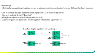
▪ About wire
▪Electrically connect things together i.e., act as an interconnection mechanism between different hardware elements
▪ Can be used on the right-hand side of an expression i.e., it is said to be driven
▪ Can have multiple drivers' “Fan-Out”
▪ Multiple drivers are resolved using resolution table
▪ Used to tie gates and behavioral blocks together defaults to a logic value ‘z’
18.
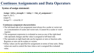
Continuos Assignments andData Operators
Syntax of assign statement:
Assign < drive_strength > < delay > < list_of_assignment >
input A, B, C;
output Y;
Assign Y = ~(A & B) | C
Continuous assignment characteristics:
▪ The left-hand side of an assignment must always be a scalar or vector net
or a concatenation of scalar and vector nets. It cannot be a scalar or vector
register.
▪ The assignment expression is evaluated as soon as one of the right-hand
side operands changes and the value is assigned to left hand side.
▪ The operands on right hand side can be registers or nets or function calls.
Registers or nets can be scalars or vectors.
▪ Delay values can be specified for assignments in terms of time units. Delay
values are used to control the time when a net is assigned the evaluated
value.
19.
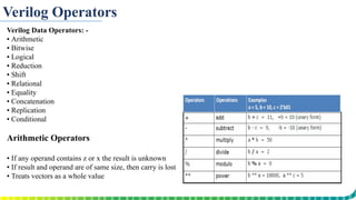
Verilog Operators
Verilog DataOperators: -
▪ Arithmetic
▪ Bitwise
▪ Logical
▪ Reduction
▪ Shift
▪ Relational
▪ Equality
▪ Concatenation
▪ Replication
▪ Conditional
Arithmetic Operators
▪ If any operand contains z or x the result is unknown
▪ If result and operand are of same size, then carry is lost
▪ Treats vectors as a whole value
20.
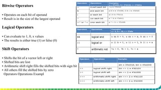
Bitwise Operators
▪ Operateson each bit of operand
▪ Result is in the size of the largest operand
Logical Operators
▪ Can evaluate to 1, 0, x values
▪ The results is either true (1) or false (0)
Shift Operators
▪ Shifts the bit of a vector left or right
▪ Shifted bits are lost
▪ Arithmetic shift right fills the shifted bits with sign bit
▪ All others fill the shifted bits by zero
Operators Operations Exampl
21.
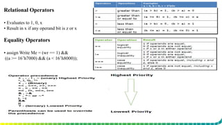
Relational Operators
▪ Evaluatesto 1, 0, x
▪ Result in x if any operand bit is z or x
Equality Operators
▪ assign Write Me = (wr == 1) &&
((a >= 16’h7000) && (a < 16’h8000));
22.
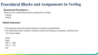
Procedural Blocks andAssignments in Verilog
Structured Procedures: -
There are two structured procedure statements in Verilog
▪ always
▪ Initial
Initial Statement
▪ All statement inside the initial statement constitute an initial block.
▪ An initial block starts at time 0, executes exactly once during a simulation, and then does
not execute again.
initial
begin
#10 x = 1'b0;
#25 y = 1'b1;
end
23.
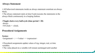
Always Statement
▪ Allbehavioral statements inside an always statement constitute an always
block.
▪ The always statement starts at time 0 and executes the statements in the
always block continuously in a looping fashion.
//Toggle clock every half-cycle (time period = 20)
always
#10 clock = ~clock;
Procedural Assignments
Syntax:
<assignment> :: = <!value> = <expression>
▪ Procedural assignments update values of reg, integer, real, or time
variables.
▪ The value placed on a variable will remain unchanged until another
procedural assignment updates the variable with a different value.
25.
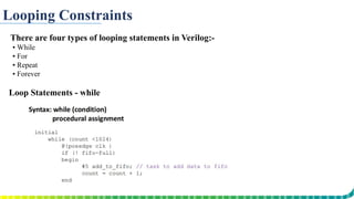
Looping Constraints
There arefour types of looping statements in Verilog:-
▪ While
▪ For
▪ Repeat
▪ Forever
Loop Statements - while
26.
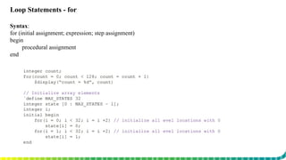
Loop Statements -for
Syntax:
for (initial assignment; expression; step assignment)
begin
procedural assignment
end
27.
Loop Statements -repeat
▪ Keyword repeat is used for this loop.
▪ Executes the loop for fixed number of times.
Loop Statements - forever
Looping statements appear inside procedural
blocks only.
The forever loop executes continuously
i.e. the loop never ends
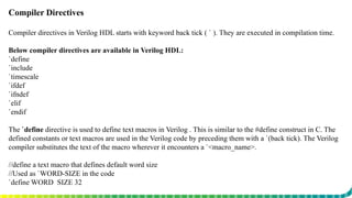
Compiler Directives
Compiler directivesin Verilog HDL starts with keyword back tick ( ` ). They are executed in compilation time.
Below compiler directives are available in Verilog HDL:
`define
`include
`timescale
`ifdef
`ifndef
`elif
`endif
The `define directive is used to define text macros in Verilog . This is similar to the #define construct in C. The
defined constants or text macros are used in the Verilog code by preceding them with a `(back tick). The Verilog
compiler substitutes the text of the macro wherever it encounters a `<macro_name>.
//define a text macro that defines default word size
//Used as `WORD-SIZE in the code
`define WORD_SIZE 32
31.
The `include directiveallows you to include entire contents of a Verilog source file in another Verilog file
during compilation. This works similarly to the #include in the C programming language. This directive is
typically used to include header files, which typically contain global or commonly used definitions
// Include the file header.v, which contains declarations in the
// main verilog file design.v.
`include header.v
...
...
<Verilog code in the file design.v>
...
`Often, in a single simulation, delay values in one module need to be defined by using certain time unit, e.g., 1
us, and delay values in another module need to be defined by using a different time unit, e.g., 100 ns. Verilog
HDL allows the reference time unit for modules to be specified with the ' timescale compiler directive.
Conditional compilation can be accomplished by using compiler directives `ifdef, `else, and
`endif. Verilog source code to be compiled conditionally.
32.
//Conditional Compilation
//Example 1
`ifdefTEST // compile module test only if text macro TEST is defined
module test;
...
endmodule
'else //compile the module stimulus as default
module stimulus;
...
...
endmodule
Array Locator Methods
find(): returns all elements
find_index(): returns all indexes of array
find_first(): returns first element
find_first_index(): returns index of first element
find_last(): returns last element
find_last_index(): returns index of last element
int d [ ] = `{2,3,4,56,67,45,4};
tqueue [ $ ];
initial begin
tqueue = d.find with (item > 3);
tqueue = d.find_last_index with (item == 4);
end
41.
Array Reduction Methods
These methods are used to reduce and unpacked array in single value.
sum(): return the sum of all elements of array
product(): return the sum of all elements of array
and(): return the sum of all elements of array
or(): return the sum of all elements of array
xor(): return the sum of all elements of array
int d [ ] = `{2,3,4,56,67,45,4};
int summ, productt;
initial begin
summ = b.sum;
productt = product;
end


![Modeling Styles
Verilog is both, behavioral and structural language. Designs in Verilog can be described at all the four
levels of abstraction depending on needs of design.
Behavioral Level: -
Used to model behavior of design without concern for the hardware implementation details. Designing at
this level is very similar to C programming.
Dataflow Level [RTL]: -
Module is specified by specifying the data flow. The designer is aware of how the data flows between
registers.
Gate Level: -
Module is implemented in terms of logic gates & interconnections between them. Design at this level is
similar to describing design in terms of gate level logical diagram.
Switch Level: -
lowest level of abstraction provided by Verilog. Module can be implemented in terms of switches, storage
nodes & interconnection between them.](https://image.slidesharecdn.com/4bd22ec412vlsi-250304054255-07e1ad22/85/very-large-scale-integration-ppt-vlsi-pptx-7-320.jpg)
![Array Locator Methods
find(): returns all elements
find_index(): returns all indexes of array
find_first(): returns first element
find_first_index(): returns index of first element
find_last(): returns last element
find_last_index(): returns index of last element
int d [ ] = `{2,3,4,56,67,45,4};
tqueue [ $ ];
initial begin
tqueue = d.find with (item > 3);
tqueue = d.find_last_index with (item == 4);
end](https://image.slidesharecdn.com/4bd22ec412vlsi-250304054255-07e1ad22/85/very-large-scale-integration-ppt-vlsi-pptx-40-320.jpg)
![Array Reduction Methods
These methods are used to reduce and unpacked array in single value.
sum(): return the sum of all elements of array
product(): return the sum of all elements of array
and(): return the sum of all elements of array
or(): return the sum of all elements of array
xor(): return the sum of all elements of array
int d [ ] = `{2,3,4,56,67,45,4};
int summ, productt;
initial begin
summ = b.sum;
productt = product;
end](https://image.slidesharecdn.com/4bd22ec412vlsi-250304054255-07e1ad22/85/very-large-scale-integration-ppt-vlsi-pptx-41-320.jpg)