![2016MVE 006 2016
MDDV Lab Manual Page 5
Code for 32 bit Full adder
////////////////////////////////////////////////////////////////////////////
// Company:
// Engineer:
// Create Date: 13:53:20 12/05/2016
// Design Name:
// Module Name: bit_32_adder
// Project Name:
// Target Devices:
// Tool versions:
// Description:
// Dependencies:
// Revision:
// Revision 0.01 - File Created
// Additional Comments:
////////////////////////////////////////////////////////////////////////////
module bit_32_adder (Sum,Cout,A,B,Cin);
parameter N=32;
input [N-1:0] A;
input [N-1:0] B;
input Cin;
output [N-1:0] Sum;
output Cout;
wire [N:0]C;
genvar i;
assign C[0]=Cin;
generate
for (i=0; i< 32; i=i+1)
begin: full_adder_cell
full_adder FA1(.sum(Sum[i]),.carry(C[i+1]),.a(A[i]),.b(B[i]),.c(C[i]));
end
endgenerate
assign Cout=C[N];
endmodule](https://image.slidesharecdn.com/2016mve006-170226092549/85/Verilog-lab-mauual-5-320.jpg)
![2016MVE 006 2016
MDDV Lab Manual Page 7
Test Bench for 32 bit adder:
//////////////////////////////////////////////////////////////////////////
// Company:
// Engineer:
// Create Date: 13:56:15 12/05/2016
// Design Name: bit_32_adder
// Module Name: D:/terminator/ripplecarryadder/tb_cra.v
// Project Name: ripplecarryadder
// Target Device:
// Tool versions:
// Description:
// Verilog Test Fixture created by ISE for module: bit_32_adder
// Dependencies:
// Revision:
// Revision 0.01 - File Created
// Additional Comments:
////////////////////////////////////////////////////////////////////////////
module tb_cra;
// Inputs
reg [31:0] A;
reg [31:0] B;
reg Cin;
// Outputs
wire [31:0] Sum;
wire Cout;
// Instantiate the Unit Under Test (UUT)
bit_32_adder uut (
.Sum(Sum),
.Cout(Cout),
.A(A),
.B(B),
.Cin(Cin)
);
initial begin
// Initialize Inputs
A = 32'd1245789613858;
B = 32'd1245789613858;
Cin = 1;
// Wait 100 ns for global reset to finish
#1000;
A = 32'd33245789613858;
B = 32'd1245789613858;
Cin = 1;](https://image.slidesharecdn.com/2016mve006-170226092549/85/Verilog-lab-mauual-7-320.jpg)
![2016MVE 006 2016
MDDV Lab Manual Page 9
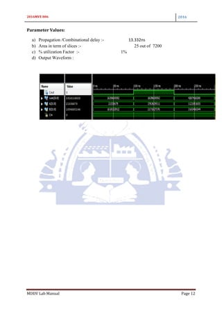
PRACTICAL NO 2
Aim:-Design & implementation of carry look ahead generator for given number of input
bits and observe, calculate following parameter
1.RTL schematic,
2.Propagration delay,
3.Number of slices in terms of % utilization,
4.Write test bench & verify timing behaviour carry look ahead generator
Design Properties:
Family - VERTEX 5 FPGA
Device - XC5VLX50T
Simulator - ISIM
Verilog Code:
Main code
////////////////////////////////////////////////////////////////////////////
// Company:
// Engineer:
//Create Date: 14:28:15 12/05/2016
// Design Name:
// Module Name: CLA_add
// Project Name:
// Target Devices:
// Tool versions:
// Description:
// Dependencies:
// Revision:
// Revision 0.01 - File Created
// Additional Comments:
////////////////////////////////////////////////////////////////////////////
module CLA_add (A, B, Cin,Cout, sum );
parameter N=32;
input [N-1:0]A,B;
input Cin;
output [N-1:0] sum;
output Cout;
wire [N:0]c;
wire [N-1:0]g,p;
assign c[0]=Cin;
genvar i;
generate
for(i=0;i<N;i=i+1)](https://image.slidesharecdn.com/2016mve006-170226092549/85/Verilog-lab-mauual-9-320.jpg)
![2016MVE 006 2016
MDDV Lab Manual Page 10
begin: CLA
carry_generate A1(.G(g[i]),.A(A[i]),.B(B[i]));
carry_propagate A2(.P(p[i]),.A(A[i]),.B(B[i]));
sum_CLA S1(.S(sum[i]),.A(c[i]),.B(p[i]));
assign c[i+1]=(g[i]|(p[i]&c[i]));
end
assign Cout=c[N];
endgenerate
endmodule
1.Program for Sum
module sum_CLA( input A,B, output S );
assign S=A^B;
endmodule
2.Program for Carry propagate
Module carry_propagate(
input A,B,
output P
);
assign P=(A^B);
endmodule
3.Program for Carry generate
Module carry_generate(
input A,B,
output G
);
assign G= (A&B);
endmodule
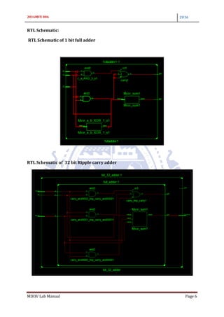
RTL Schematic:](https://image.slidesharecdn.com/2016mve006-170226092549/85/Verilog-lab-mauual-10-320.jpg)
![2016MVE 006 2016
MDDV Lab Manual Page 11
Test bench:-
module tb_CLA;
// Inputs
reg [31:0] A;
reg [31:0] B;
reg Cin;
// Outputs
wire Cout;
wire [31:0] sum;
// Instantiate the Unit Under Test (UUT)
CLA_add uut (
.A(A),
.B(B),
.Cin(Cin),
.Cout(Cout),
.sum(sum)
);
initial begin
// Initialize Inputs
A = 32'd568795425447847;
B = 32'd58795425447856;
Cin = 1;
// Wait 100 ns for global reset to finish
#100;
A = 32'd368795425447847;
B = 32'd258795425447856;
Cin = 1;
// Wait 100 ns for global reset to finish
#100;
A = 32'd86875425447847;
B = 32'd95875425447856;
Cin = 1;
// Wait 100 ns for global reset to finish
#100;
A = 32'd568795425447847;
B = 32'd158795425447856;
Cin = 0;
// Wait 100 ns for global reset to finish
#100;
// Add stimulus here
end
endmodule](https://image.slidesharecdn.com/2016mve006-170226092549/85/Verilog-lab-mauual-11-320.jpg)
![2016MVE 006 2016
MDDV Lab Manual Page 13
PRACTICAL NO 3
Aim:-Design & implementation of carry select adder for given number of input bits and
observe, calculate following parameter
1.RTL schematic,
2.Propagration delay,
3.Number of slices in terms of % utilization,
4.Write test bench & verify timing behaviour carry select adder
Design Properties:
Family - VERTEX 5 FPGA
Device - XC5VLX50T
Simulator - ISIM
Verilog Code:
Main code:
////////////////////////////////////////////////////////////////////////////
// Company:
// Engineer:
// Create Date: 15:36:11 5/12/2016
// Design Name:
// Module Name: CSA
// Project Name:
// Target Devices:
// Tool versions:
// Description:
// Revision:
// Revision 0.01 - File Created
// Additional Comments:
////////////////////////////////////////////////////////////////////////////
module CSA(A,B,Cin,S, Cout);
parameter N=32;
input [N-1:0]A,B;
input Cin;
output [N-1:0]S;
output Cout;
wire [N:0] c;
wire [N:1] c0,c1;
wire [N-1:0] sum0,sum1;
assign c[0]=Cin;
// assign c1[0]=1;
//assign c0[0]=0;
genvar i;](https://image.slidesharecdn.com/2016mve006-170226092549/85/Verilog-lab-mauual-13-320.jpg)
![2016MVE 006 2016
MDDV Lab Manual Page 14
generate
for(i=0;i<N;i=i+1)
begin: CSA
ha_1213 A1(.s(sum0[i]),.c(c0[i+1]),.a(A[i]),.b(B[i]));
full_adder X2(.s(sum1[i]),.cout(c1[i+1]),.a(A[i]),.b(B[i]),.cin(1));
mux_CSA M1(.sum(S[i]),.s0(sum0[i]),.s1(sum1[i]),.c(c[i]));
mux_CSA M2(.sum(c[i+1]),.s0(c0[i+1]),.s1(c1[i+1]),.c(c[i]));
end
assign Cout=(c[32]== 1'b0)? c0[32]:c1[32];
endgenerate
endmodule
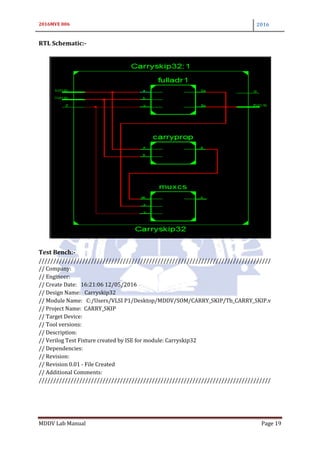
RTL schematic:-
Testbench for CSA
module CSA_tb;
// Inputs
reg [31:0] A;
reg [31:0] B;
reg Cin;](https://image.slidesharecdn.com/2016mve006-170226092549/85/Verilog-lab-mauual-14-320.jpg)
![2016MVE 006 2016
MDDV Lab Manual Page 15
// Outputs
wire [31:0] S;
wire Cout;
// Instantiate the Unit Under Test (UUT)
CSA uut (
.A(A),
.B(B),
.Cin(Cin),
.S(S),
.Cout(Cout)
);
initial begin
// Initialize Inputs
A = 32'h5446341;
B = 32'h3854487;
Cin = 0;
// Wait 100 ns for global reset to finish
#100;
A = 32'h563471;
B = 32'h38843;
// Wait 100 ns for global reset to finish
#100;
A = 32'h5566341;
B = 32'h386787;
Cin = 1;
// Wait 100 ns for global reset to finish
#100;
A = 32'h453743;
B = 32'h3427fff;
Cin = 0;
// Wait 100 ns for global reset to finish
#100;
A = 32'hffffffff;
B = 32'h1;
Cin = 0;
// Wait 100 ns for global reset to finish
#100;
// Add stimulus here](https://image.slidesharecdn.com/2016mve006-170226092549/85/Verilog-lab-mauual-15-320.jpg)
![2016MVE 006 2016
MDDV Lab Manual Page 17
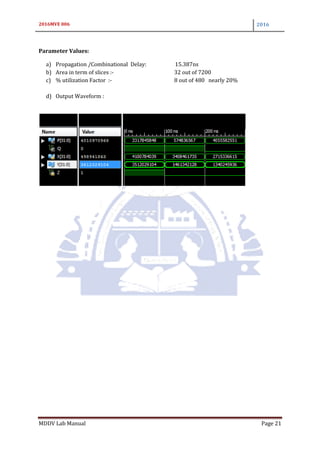
PRACTICAL NO 4
Aim:- Design & implementation of Carry Skip Adder for given number of input bits and
observe, calculate following parameter
1.RTL schematic,
2.Propagration delay,
3.Number of slices in terms of % utilization,
4.Write test bench & verify timing behaviour
Design Properties:
Family - VERTEX 5 FPGA
Device - XC5VLX50T
Simulator - ISIM
Verilog Code:
Main code:
////////////////////////////////////////////////////////////////////////////
// Company:
// Engineer:
// Create Date: 15:38:04 12/05/2016
// Design Name:
// Module Name: Carry_skip32
// Project Name:
// Target Devices:
// Tool versions:
// Description:
// Dependencies:
// Revision:
// Revision 0.01 - File Created
// Additional Comments:
////////////////////////////////////////////////////////////////////////////
module Carry_skip32(X,Y,Z,P,Q);
parameter N=32;
input[N-1:0]X,Y;
input Z;
output[N-1:0]P;
output Q;
wire [N-1:0]w1,w2;
wire [N:0]C;
assign C[0]=Z;
genvar i;
generate](https://image.slidesharecdn.com/2016mve006-170226092549/85/Verilog-lab-mauual-17-320.jpg)
![2016MVE 006 2016
MDDV Lab Manual Page 18
for(i=0;i<N;i=i+1)
begin: Carryskip32
fulladr1 A1(.a(X[i]),.b(Y[i]),.c(C[i]),.Su(P[i]),.Co(w1[i]));
carryprop A2(.a(X[i]),.b(Y[i]),.p(w2[i]));
muxcs A3(.x(w1[i]),.y(C[i]),.se(w2[i]),.z(C[i+1]));
end
assign Q=C[32];
endgenerate
endmodule
Sub-module
1. Full Adder:
module fulladr1(
input a,b,c,
output Su,Co
);
assign Su=a^b^c;
assign Co=((a&b)|(b&c)|(c&a));
endmodule
2. Mux
module muxcs(
input x,y,se,
output z
);
assign z=(se==1'b0)?x:y;
endmodule
3. Carry propagation
module carryprop(
input a,b,
output p
);
assign p=a^b;
endmodule](https://image.slidesharecdn.com/2016mve006-170226092549/85/Verilog-lab-mauual-18-320.jpg)
![2016MVE 006 2016
MDDV Lab Manual Page 20
module Tb_CARRY_SKIP;
// Inputs
reg [31:0] X;
reg [31:0] Y;
reg Z;
// Outputs
wire [31:0] P;
wire Q;
// Instantiate the Unit Under Test (UUT)
Carryskip32 uut (
.X(X),
.Y(Y),
.Z(Z),
.P(P),
.Q(Q)
);
initial begin
// Initialize Inputs
X = 32'd76875425447847;
Y = 32'd65875425447856;
Z = 1;
// Wait 100 ns for global reset to finish
#100;
X = 32'd12875425447847;
Y = 32'd94675425447856;
Z = 0;
// Wait 100 ns for global reset to finish
#100;
X = 32'd72875425447847;
Y = 32'd74175425447856;
Z = 0;
// Wait 100 ns for global reset to finish
#100;
// Add stimulus here
end
endmodule](https://image.slidesharecdn.com/2016mve006-170226092549/85/Verilog-lab-mauual-20-320.jpg)
![2016MVE 006 2016
MDDV Lab Manual Page 22
PRACTICAL NO 5
Aim:- Design & implementation of Carry Save Adder for given number of input bits and
observe, calculate following parameter
1.RTL schematic,
2.Propagration delay,
3.Number of slices in terms of % utilization,
4.Write test bench & verify timing behaviour
Design Properties:
Family - VERTEX 5 FPGA
Device - XC5VLX50T
Simulator - ISIM
Verilog Code:
Main code:
////////////////////////////////////////////////////////////////////////////
// Company:
// Engineer:
// Create Date: 16:36:15 12/05/2016
// Design Name:
// Module Name: carry_save
// Project Name:
// Target Devices:
// Tool versions:
// Description:
// Dependencies:
// Revision:
// Revision 0.01 - File Created
// Additional Comments:
////////////////////////////////////////////////////////////////////////////
module carry_save( X,Y,Z,S,Cout);
parameter N=32;
input[N-1:0]X,Y,Z;
output[N:0]S;
output Cout;
wire [N:0]l;
wire [N-1:0]m;
wire[N+1:0]w;
assign l[0]=0;
assign w[0]=0;
genvar i;](https://image.slidesharecdn.com/2016mve006-170226092549/85/Verilog-lab-mauual-22-320.jpg)
![2016MVE 006 2016
MDDV Lab Manual Page 23
generate
for(i=0;i<N;i=i+1)
begin: Carrysave32
fulladr1 A3(.x(X[i]),.y(Y[i]),.z(Z[i]),.u(m[i]),.v(l[i+1]));
fulladr1 A4(.x(l[i]),.y(m[i]),.z(w[i]),.u(S[i]),.v(w[i+1]));
end
assign S[32]=w[32]^l[32];
assign Cout=w[32]&l[32];
endgenerate
endmodule
RTL Schematic:-](https://image.slidesharecdn.com/2016mve006-170226092549/85/Verilog-lab-mauual-23-320.jpg)
![2016MVE 006 2016
MDDV Lab Manual Page 24
Test Bench:-
module TB_CARRY_SAVEADDER;
// Inputs
reg [31:0] X;
reg [31:0] Y;
reg [31:0] Z;
// Outputs
wire [32:0] S;
wire Cout;
// Instantiate the Unit Under Test (UUT)
carry_save uut (
.X(X),
.Y(Y),
.Z(Z),
.S(S),
.Cout(Cout)
);
initial begin
// Initialize Inputs
X = 32'd22875425447847;
Y = 32'd84675425447856;
Z = 1;
// Wait 100 ns for global reset to finish
#100;
X = 32'd21875425447847;
Y = 32'd49675425447856;
Z = 0;
// Wait 100 ns for global reset to finish
#100;
X = 32'd55875425447847;
Y = 32'd33675425447856;
Z = 1;
// Wait 100 ns for global reset to finish
#100;
X = 32'd85275425447847;
Y = 32'd25875425447856;
Z = 0;
// Wait 100 ns for global reset to finish
#100;
X = 32'd82175425447847;](https://image.slidesharecdn.com/2016mve006-170226092549/85/Verilog-lab-mauual-24-320.jpg)
![2016MVE 006 2016
MDDV Lab Manual Page 27
PRACTICAL NO 6
Aim:- Design & implementation of Add_Shift_Multiplier for given number of input bits
and observe, calculate following parameter
1.RTL schematic,
2.Propagration delay,
3.Number of slices in terms of % utilization,
4.Write test bench & verify timing behaviour .
Design Properties:
Family - VERTEX 5 FPGA
Device - XC5VLX50T
Simulator - ISIM
Verilog Code:
Main code:
////////////////////////////////////////////////////////////////////////////
// Company:
// Engineer:
//
// Create Date: 17:16:10 12/05/2016
// Design Name:
// Module Name: Add_Shift_mul
// Project Name:
// Target Devices:
// Tool versions:
// Description:
// Dependencies:
// Revision:
// Revision 0.01 - File Created
// Additional Comments:
////////////////////////////////////////////////////////////////////////////
module Add_Shift_mul(
input [3:0] A,B,
output [7:0] S
);
wire [16:0]o;
wire [14:0]i;
And12 A1(.z(S[0]),.x(A[0]),.y(B[0]));
And12 A2(.z(i[0]),.x(A[1]),.y(B[0]));
And12 A3(.z(i[1]),.x(A[0]),.y(B[1]));
And12 A4(.z(i[2]),.x(A[0]),.y(B[2]));
And12 A5(.z(i[3]),.x(A[1]),.y(A[1]));](https://image.slidesharecdn.com/2016mve006-170226092549/85/Verilog-lab-mauual-27-320.jpg)
![2016MVE 006 2016
MDDV Lab Manual Page 28
And12 A6(.z(i[4]),.x(A[2]),.y(B[0]));
And12 A7(.z(i[5]),.x(A[0]),.y(B[3]));
And12 A8(.z(i[6]),.x(A[1]),.y(B[2]));
And12 A9(.z(i[7]),.x(A[2]),.y(B[1]));
And12 A10(.z(i[8]),.x(A[3]),.y(B[0]));
And12 A11(.z(i[9]),.x(A[1]),.y(B[3]));
And12 A12(.z(i[10]),.x(A[2]),.y(B[2]));
And12 A13(.z(i[11]),.x(A[3]),.y(B[1]));
And12 A14(.z(i[12]),.x(A[2]),.y(B[3]));
And12 A15(.z(i[13]),.x(A[3]),.y(B[2]));
And12 A16(.z(i[14]),.x(A[3]),.y(B[3]));
Halfadr H1(.s(S[1]),.c(o[0]),.a(i[0]),.b(i[1]));
Halfadr H2(.s(o[1]),.c(o[2]),.a(i[2]),.b(i[3]));
Halfadr H3(.s(o[3]),.c(o[4]),.a(i[5]),.b(i[6]));
fulladdr F1(.s(S[2]),.t(o[5]),.p(o[0]),.q(o[1]),.r(i[4]));
fulladdr F2(.s(o[6]),.t(o[7]),.p(o[2]),.q(o[3]),.r(i[7]));
fulladdr F3(.s(S[3]),.t(o[8]),.p(o[5]),.q(o[6]),.r(i[8]));
fulladdr F4(.s(o[9]),.t(o[10]),.p(i[9]),.q(i[10]),.r(o[4]));
fulladdr F5(.s(o[11]),.t(o[12]),.p(o[9]),.q(i[11]),.r(o[7]));
Halfadr H4(.s(S[4]),.c(o[13]),.a(o[11]),.b(o[8]));
fulladdr F6(.s(o[14]),.t(o[15]),.p(i[13]),.q(i[12]),.r(o[10]));
fulladdr F7(.s(S[5]),.t(o[16]),.p(o[12]),.q(o[14]),.r(o[13]));
fulladdr F8(.s(S[6]),.t(S[7]),.p(o[16]),.q(o[15]),.r(i[14]));
endmodule
Sub_module:-
1.And Gate
module And12(
input x,y,
output z
);
assign z=x&y;
endmodule
2.Full Adder:-
module fulladdr(
input p,q,r,
output s,t );
assign s=p^q^r;
assign t=((p&q)|(q&r)|(p&r));
endmodule](https://image.slidesharecdn.com/2016mve006-170226092549/85/Verilog-lab-mauual-28-320.jpg)
![2016MVE 006 2016
MDDV Lab Manual Page 30
Test Bench:-
module Tb_Add_Shift_Mul;
// Inputs
reg [3:0] A;
reg [3:0] B;
// Outputs
wire [7:0] S;
// Instantiate the Unit Under Test (UUT)
Add_Shift_mul uut (
.A(A),
.B(B),
.S(S)
);
initial begin
// Initialize Inputs
A = 4'b1100;
B = 4'b1100;
// Wait 100 ns for global reset to finish
#100;
A = 4'b1100;
B = 4'b1100;
// Wait 100 ns for global reset to finish
#100;
A = 4'b1010;
B = 4'b1111;
// Wait 100 ns for global reset to finish
#100;
A = 4'b1001;
B = 4'b1001;
// Wait 100 ns for global reset to finish
#100;
A = 4'b1000;
B = 4'b1000;
// Wait 100 ns for global reset to finish
#100;
// Add stimulus here
end
endmodule](https://image.slidesharecdn.com/2016mve006-170226092549/85/Verilog-lab-mauual-30-320.jpg)
![2016MVE 006 2016
MDDV Lab Manual Page 32
PRACTICAL NO 7
Aim:- Design & implementation of Carry Save Multiplier for given number of input bits
and observe, calculate following parameter
1.RTL schematic,
2.Propagration delay,
3.Number of slices in terms of % utilization,
4.Write test bench & verify timing behaviour .
Design Properties:
Family - VERTEX 5 FPGA
Device - XC5VLX50T
Simulator - ISIM
Verilog Code:-
module carry_save_mul(
input [3:0] A,B,
output [7:0] P
);
wire [19:0]w;
andgate A1(.a(A[0]),.b(B[0]),.c(P[0]));
andgate A2(.a(A[0]),.b(B[1]),.c(w[0]));
andgate A3(.a(A[0]),.b(B[2]),.c(w[1]));
andgate A4(.a(A[0]),.b(B[3]),.c(w[2]));
hadr H1(.a(w[0]),.b(A[1]&B[0]),.s(P[1]),.c(w[3]));
hadr H2(.a(w[1]),.b(A[1]&B[1]),.s(w[4]),.c(w[5]));
hadr H3(.a(w[2]),.b(A[1]&B[2]),.s(w[6]),.c(w[7]));
hadr H4(.a(w[17]),.b(A[1]&B[3]),.s(w[8]),.c(w[9]));
fulladr F1(.x(w[4]),.z(w[3]),.y(A[2]&B[0]),.p(P[2]),.q(w[10]));
fulladr F2(.x(w[6]),.y(A[2]&B[1]),.z(w[5]),.p(w[11]),.q(w[12]));
fulladr F3(.x(w[8]),.y(A[2]&B[2]),.z(w[7]),.p(w[13]),.q(w[14]));
fulladr F4(.x(w[18]),.y(A[2]&B[3]),.z(w[9]),.p(w[15]),.q(w[16]));
fulladr F5(.x(w[11]),.y(A[3]&B[0]),.z(w[10]),.p(P[3]),.q(w[17]));
fulladr F6(.x(w[13]),.y(A[3]&B[1]),.z(w[12]),.p(P[4]),.q(w[18]));
fulladr F7(.x(w[15]),.y(A[3]&B[2]),.z(w[14]),.p(P[5]),.q(w[19]));
fulladr F8(.x(w[19]),.y(A[3]&B[3]),.z(w[16]),.p(P[6]),.q(P[7]));
endmodule](https://image.slidesharecdn.com/2016mve006-170226092549/85/Verilog-lab-mauual-32-320.jpg)
![2016MVE 006 2016
MDDV Lab Manual Page 34
Test Bench:-
module Tb_Carry_save_Mul;
// Inputs
reg [3:0] A;
reg [3:0] B;
// Outputs
wire [7:0] P;
// Instantiate the Unit Under Test (UUT)
carry_save_mul uut (
.A(A),
.B(B),
.P(P)
);
initial begin
// Initialize Inputs
A = 4'b1100;
B = 4'b1100;
// Wait 100 ns for global reset to finish
#100;
A = 4'b1010;
B = 4'b1111;
// Wait 100 ns for global reset to finish
#100;
A = 4'b1011;
B = 4'b1010;
// Wait 100 ns for global reset to finish
#100;
A = 4'b1010;
B = 4'b1101;
// Wait 100 ns for global reset to finish
#100;
// Add stimulus here
end
Endmodule](https://image.slidesharecdn.com/2016mve006-170226092549/85/Verilog-lab-mauual-34-320.jpg)
![2016MVE 006 2016
MDDV Lab Manual Page 36
Practical 8: Booths Multiplier
Aim: Design and implementation of Booths multiplier for given number of input bits.
Verilog Codes for Booths Multiplier
module own_booths( a,b,y,sign);
parameter N=16, P=N/2; // N = no of inputsP= no of groups
output reg sign;
input [N-1:0] a,b; // a= multiplier b= multiplicant
output [(N+N-1):0]y;
integer k,i;
reg [2:0] m [P-1:0];
reg [(N+N-1):0] b1 [P-1:0];
reg [(N+N-1):0] z [P-1:0];
reg [(N+N-1):0]z1;
always @ (a or b ) begin
m[0]={a[1],a[0],1'b0};
for(k=1;k<P;k=k+1) begin
m[k]={a[2*k+1],a[2*k],a[2*k-1]};
end
for (k=0; k<P; k=k+1) begin
case(m[k])
3'b000: b1[k]=0;
3'b001: b1[k]=b;
3'b010: b1[k]=b;
3'b011: b1[k]=b*2;
3'b100: b1[k]=b*(-2);
3'b101: b1[k]=b*(-1);
3'b110: b1[k]=b*(-1);
3'b111: b1[k]=0;
endcase
z[k]= $signed(b1[k]);
for (i=0; i<k; i=i+1) begin
z[k]={z[k],2'b00};
end
end
z1=z[0];
for (k=1; k<P; k=k+1) begin
z1 = z1 + z[k];
sign=0;
end
if(z1[2*N-1]==1) begin
z1= (~z1 + 1'b1);
sign=1;
end
end
assign y = z1;
endmodule](https://image.slidesharecdn.com/2016mve006-170226092549/85/Verilog-lab-mauual-36-320.jpg)
![2016MVE 006 2016
MDDV Lab Manual Page 37
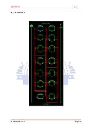
RTL Schematic for Booths Multiplier:-
Testbench
`
module Tb_Booths_mul;
// Inputs
reg [15:0] a;
reg [15:0] b;
// Outputs
wire [31:0] y;
wire sign;
// Instantiate the Unit Under Test (UUT)
Booth_Mul uut (
.a(a),
.b(b),
.y(y),
.sign(sign)
);](https://image.slidesharecdn.com/2016mve006-170226092549/85/Verilog-lab-mauual-37-320.jpg)
![2016MVE 006 2016
MDDV Lab Manual Page 40
Practical 9: Floating Point Adder
Aim: Design and implementation of floating point Adder for given number of input bits.
Verilog Code for Floating Point Adder
module fpadd(a,b,clk,out);
input[31:0]a,b;
input clk;
output [31:0]out;
wire [7:0]e1,e2,ex,ey,exy,ex1,ey1,ex2,ex3;
wire s1,s2,s,s3,sr,sn,s4,sx1,sy1,sn1,sn2,sn3,sn4,sr1,sr2,sn5,sn6;
wire [23:0]m1,m2,mx,my,mxy,mx1,my1;
wire [24:0]mxy1,mxy2;
assign s1=a[31];
assign s2=b[31];
assign e1=a[30:23];
assign e2=b[30:23];
assign m1[23]=1'b1;
assign m2[23]=1'b1;
assign m1[22:0]=a[22:0];
assign m2[22:0]=b[22:0];
//submodule for compare and shfit
cmpshift as(e1[7:0],e2[7:0],s1,s2,m1[23:0],m2[23:0],clk,ex,ey,mx,my,s,sx1,sy1);
buffer1 buff1(ex,ey,sx1,sy1,mx,my,s,clk,ex1,ey1,mx1,my1,sn,sn1,sn2);
//sub module for mantissa addition snd subtraction
faddsub as1(mx1,my1,sn1,sn2,sn,ex1,clk,mxy1,ex2,sn3,sn4,s3,sr1);
buffer2 buff2(mxy1,s3,sr1,ex2,sn3,sn4,clk,mxy2,ex3,sn5,sn6,s4,sr2);
//sub module for normalization
normalized as2(mxy2,sr2,sn5,sn6,s4,clk,ex3,sr,exy,mxy);
assign out={sr,exy,mxy[22:0]};
endmodule
Compare& shift module:
module cmpshift(e1,e2,s1,s2,m1,m2,clk,ex,ey,mx,my,s,sx1,sy1); //module for
copare&shift
input [7:0]e1,e2;
input [23:0]m1,m2;
input clk,s1,s2;
output reg[7:0]ex,ey;
output reg[23:0]mx,my;
output reg s,sx1,sy1;
reg [7:0]diff;](https://image.slidesharecdn.com/2016mve006-170226092549/85/Verilog-lab-mauual-40-320.jpg)
![2016MVE 006 2016
MDDV Lab Manual Page 41
always@(posedgeclk)
begin
sx1=s1;
sy1=s2;
if(e1==e2)
begin
ex=e1+8'b1;
ey=e2+8'b1;
mx=m1;
my=m2;
s=1'b1;
end
else if(e1>e2)
begin
diff=e1-e2;
ex=e1+8'b1;
ey=e1+8'b1;
mx=m1;
my=m2>>diff;
s=1'b1;
end
else
begin
diff=e2-e1;
ex=e2+8'b1;
ey=e2+8'b1;
mx=m2;
my=m1>>diff;
s=1'b0;
end
end
endmodule
faddsub module:-
module faddsub(a,b,s1,s2,sn,ex1,clk,out,ex2,sn3,sn4,s,sr1); //submodule for addition or
subtraction
input [23:0]a,b;
input[7:0]ex1;
input s1,s2,clk,sn;
output reg [7:0]ex2;
output reg[24:0]out;
output reg s,sn3,sn4,sr1;
always@(posedge clk)
begin
ex2=ex1;
sr1=sn;
sn3=s1;](https://image.slidesharecdn.com/2016mve006-170226092549/85/Verilog-lab-mauual-41-320.jpg)
![2016MVE 006 2016
MDDV Lab Manual Page 42
sn4=s2;
s=s1^s2;
if(s)
begin
out=a-b;
end
else
begin
out=a+b;
end
end
endmodule
Buffer:
module buffer2(mxy1,s3,sr1,ex,sn3,sn4,clk,mxy2,ex3,sn5,sn6,s4,sr2);
input [24:0]mxy1;
input s3,clk,sr1,sn3,sn4;
input [7:0]ex;
output reg[24:0]mxy2;
output reg[7:0]ex3;
output reg s4,sn5,sn6,sr2;
always@(posedgeclk)
begin
sr2=sr1;
sn5=sn3;
sn6=sn4;
ex3=ex;
mxy2=mxy1;
s4=s3;
end
endmodule
module buffer1(ex,ey,sx1,sy1,mx,my,s,clk,ex1,ey1,mx1,my1,sn,sn1,sn2);
input [7:0]ex,ey;
input [23:0]mx,my;
input s,clk,sx1,sy1;
output reg [7:0]ex1,ey1;
output reg [23:0]mx1,my1;
output reg sn,sn1,sn2;
always@(posedgeclk)
begin
sn1=sx1;
sn2=sy1;
ex1=ex;
ey1=ey;](https://image.slidesharecdn.com/2016mve006-170226092549/85/Verilog-lab-mauual-42-320.jpg)
![2016MVE 006 2016
MDDV Lab Manual Page 43
mx1=mx;
my1=my;
sn=s;
end
endmodule
LOD & Normalization:
module normalized(mxy1,s,s1,s2,s3,clk,ex,sr,exy,mxy);
input[24:0]mxy1;
input s,s1,s2,s3,clk;
input[7:0]ex;
output regsr;
output reg[7:0]exy;
output reg[23:0]mxy;
reg [24:0]mxy2;
always@(posedgeclk)
begin
sr=s?s1^(mxy1[24]&s3):s2^(mxy1[24]&s3);
mxy2=(mxy1[24]&s3)?~mxy1+25'b1:mxy1;
mxy=mxy2[24:1];
exy=ex;
repeat(24)
begin
if(mxy[23]==1'b0)
begin
mxy=mxy<<1'b1;
exy=exy-8'b1;
end
end
end
endmodule
RTL Schematic:-](https://image.slidesharecdn.com/2016mve006-170226092549/85/Verilog-lab-mauual-43-320.jpg)
![2016MVE 006 2016
MDDV Lab Manual Page 44
Test bench:-
module tb_FPA;
reg [31:0] a;
reg [31:0] b;
regclk;
// Outputs
wire [31:0] out;
// Instantiate the Unit Under Test (UUT)
fpadduut (
.a(a),
.b(b),
.clk(clk),
.out(out)
);
initial begin
// Initialize Inputs
a = 32'h15856378;
b = 32'h46543643;
// Wait 100 ns for global reset to finish
#100;
// Add stimulus here
end
endmodule
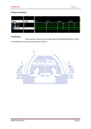
Output waveform:-
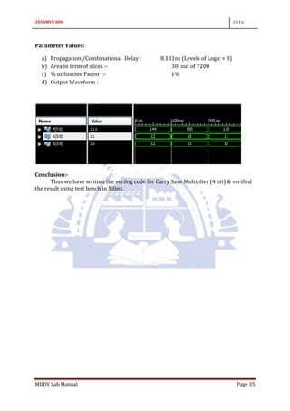
Conclusion:- Thus we have write the verilog code for floating point adder (32 bit)
pipelined structure and verified the it using test bench.](https://image.slidesharecdn.com/2016mve006-170226092549/85/Verilog-lab-mauual-44-320.jpg)
![2016MVE 006 2016
MDDV Lab Manual Page 45
Practical 10: Floating Point Multiplier
Aim: Design and implementation of floating point Multiplier for given number of input
bits.
Verilog code for Floating point multiplier
module floating(a,b,bias,out);
input[31:0]a;
input[31:0]b;
input[7:0]bias;
output[31:0]out;
wire[47:0]mo;
wire[22:0]mout;
wire[22:0]ma;
wire[22:0]mb;
wire[7:0]e1;
wire[7:0]e2;
wire[7:0]eo;
wire[7:0]eout;
wire sa,sb,so;
assign sa=a[31];
assign sb=b[31];
assign so=sa^sb;
assign e1[7:0]=a[30:23];
assign e2[7:0]=b[30:23];
assign eo[7:0]=e1+e2-bias;
assign ma[22:0]=a[22:0];
assign mb[22:0]=b[22:0];
assign mo[47:0]={1'b1,ma}*{1'b1,mb};
mantisainst (mo,eo,eout,mout);
assign out[31:0]={so,eout,mout};
endmodule
Verilog code for mantissa
module mantisa( mo,eo,eout,mout);
input[47:0]mo;
input[7:0]eo;
output[7:0]eout;
output[22:0]mout;
reg[7:0]eout;
reg[22:0]mout;
always@ (*)
begin
if(mo[47]==1)
begin
eout<=eo+1;](https://image.slidesharecdn.com/2016mve006-170226092549/85/Verilog-lab-mauual-45-320.jpg)
![2016MVE 006 2016
MDDV Lab Manual Page 46
mout<=mo[46:24];
end
else
begin
eout<=eo;
mout<=mo[45:23];
end
end
endmodule
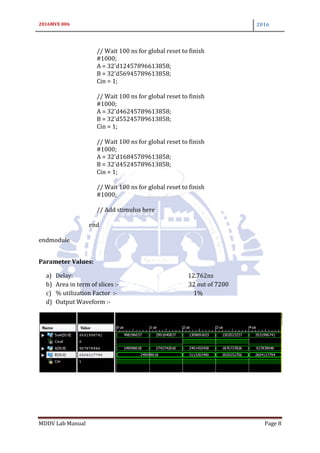
RTL Schematic:-
Parameters
Propagation Delay : 9.436ns (Levels of Logic = 6)
Area in terms of Slices: 28 out of 7200
Utilization factor : 1%](https://image.slidesharecdn.com/2016mve006-170226092549/85/Verilog-lab-mauual-46-320.jpg)
![2016MVE 006 2016
MDDV Lab Manual Page 48
Practical 11:
Aim: Design & Implement given function Sin(x), Cos(x) and ex Using Taylors series in
Questa Sim .
Verilog Code for sin(x)
module sinx(input [63:0]x, output reg[63:0] sumout);
real term=64'd1,sum=64'd1,k=64'd1,x1;
always@(x, k)
begin
x1=(x*(3.141592654/180));
if(0<k<100)
begin
term=((-1)*term*((x1*x1)/((k+1)*(k+2))));
sum<=(x1*(sum+term));
k<=k+2;
end
end
endmodule
Verilog Code for cos(x)
module cosx(input [63:0] a, output reg [63:0] sumout);
real x, term=64'd1,sum=64'd1,k=64'd1,final,x1;
always@(x, k)
begin
x1=(x*(3.141592654/180));
if(0<k<100)
begin
term=((-1)*term*((x1*x1)/((k)*(k+1))));
sum<=sum+term;
k<=k+2;
end
end
endmodule](https://image.slidesharecdn.com/2016mve006-170226092549/85/Verilog-lab-mauual-48-320.jpg)
![2016MVE 006 2016
MDDV Lab Manual Page 49
Verilog Code for eX
module exponential(input [64:0]x,output reg[64:0] sumout);
real term=64'd1,sum=64'd1,k=64'd1;
real finalsum=64'd0;
always@(x,k)
begin
if(0<k<20)
begin
term=(term*(x/k));
sum<=sum+term;
k<=k+1;
end
assign finalsum=sum;
end
endmodule
Output waveform:-
Conclusion:-
Thus we have implemented & verified the code for function Sin(x),
Cos(x) and ex Using Taylors series in Questa Sim .](https://image.slidesharecdn.com/2016mve006-170226092549/85/Verilog-lab-mauual-49-320.jpg)
![2016MVE 006 2016
MDDV Lab Manual Page 50
Practical No. 12
Aim:-Design and implement the verilog code for Questa sim for
1. Reciprocal of Number
2. Square root of Number using Newton Raphson Method.
Questa Sim :-Questa Sim is part of the Questa Advanced Functional Verification
Platform and is the latest tool in Mentor Graphics tool suite for Functional Verification.
The tool provides simulation support for latest standards of System, System Verilog,
Verilog 2001 standard and VHDL.
Verilog code for Reciprocal:-
module reciprocal (input[63:0] d,output reg[63:0] out);
real final, reci=64'd1, z=64'd1, reci1=64'd0, i ;
always @(*)
begin
final=1/z;
for(i=0;i<=5;i=i+1)
begin
if(reci==final)
begin
$display("reciprocal of x is %f ",reci);
end
else
begin
reci=(reci*(2-(z*reci)));
end
end
end
endmodule
Output Waveform:-](https://image.slidesharecdn.com/2016mve006-170226092549/85/Verilog-lab-mauual-50-320.jpg)
![2016MVE 006 2016
MDDV Lab Manual Page 51
Verilog code for Square Root:-
module sqroot(input[63:0] d,output reg[63:0] out);
real final,reci=64'd1,z=64'd1,i;
always @(*)
begin
final=1/z;
for(i=0;i<=5;i=i+1)
begin
if(reci==final)
begin
$display("reciprocal of x is %f ",reci);
end
else
begin
reci=(((reci*reci)+z)/(2*reci));
end
end
end
endmodule
Output Waveform:-
Conclusion:-
Thus we have Perform the practical & verified the code for Reciprocal
& Square root of given Number using Newton raphson’s method.](https://image.slidesharecdn.com/2016mve006-170226092549/85/Verilog-lab-mauual-51-320.jpg)

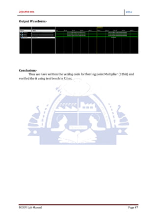
The document appears to be a lab manual describing various adder designs to be implemented and tested in Verilog, including ripple carry adders, carry lookahead adders, carry select adders, and carry skip adders. It provides Verilog code examples and test benches for 32-bit implementations of each adder type, as well as expected results for propagation delay, resource utilization, and output waveforms. The manual is meant to guide students through designing and analyzing the performance of different adder architectures.