This document discusses system organization and input/output device interfaces. It covers several topics:
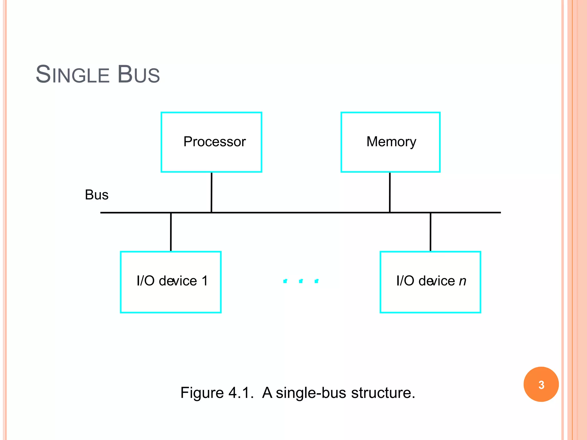
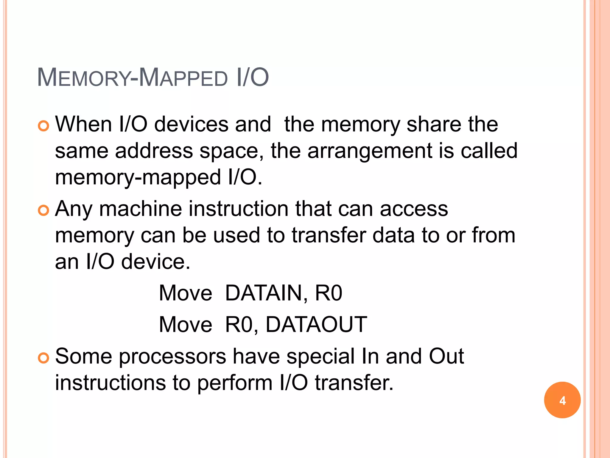
1. Single bus architecture with memory-mapped I/O and interface circuits to connect devices to the bus.
2. Program-controlled I/O using polling and interrupts to handle asynchronous devices.
3. Direct memory access (DMA) for high-speed transfer of blocks of data between memory and I/O devices.
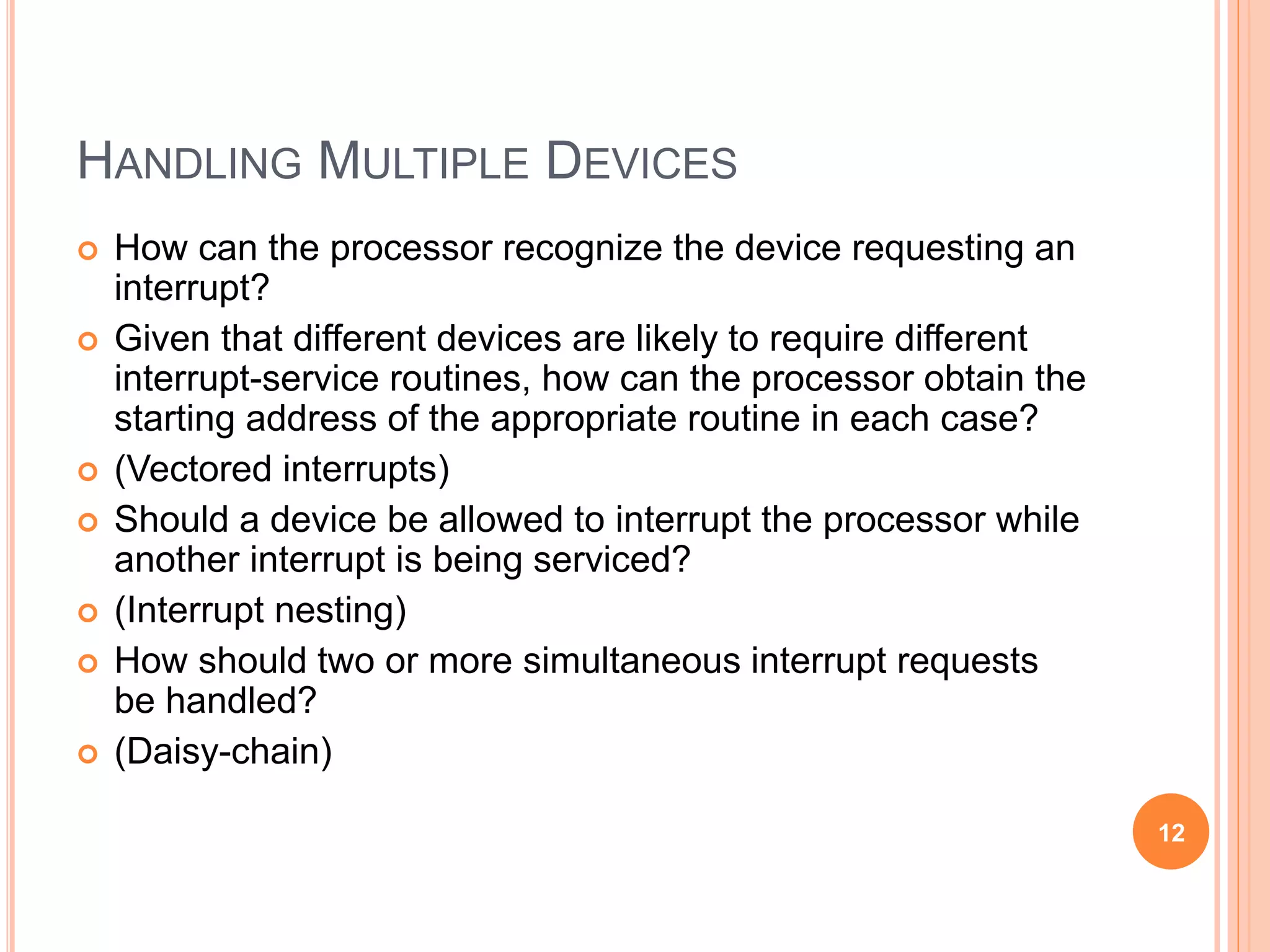
4. Details of interrupt handling including priorities, nesting, and vectored interrupts.
Arm cortex (lpc 2148) based motor speedUday Wankar
The project is designed to control the speed of a DC and AC motor using an
ARM7 LPC2148 processor. The speed of motor is directly proportional to the voltage
applied across its terminals. Hence, if voltage across motor terminal is varied, then
speed can also be varied. This project uses the above principle to control the speed of
the motor by varying the duty cycle of the pulses applied to it, popularly known as
PWM control. The project uses input button interfaced to the processor, which are
used to control the speed of motor. Pulse Width Modulation is generated at the output
by the microcontroller as per the program. The program is written in Embedded C.
The average voltage given or the average current flowing through the motor
will change depending on the duty cycle, ON and OFF time of the pulses, so the speed
of the motor will change. A motor driver IC is interfaced to the ARM7 LPC2148
processor board for receiving PWM signals and delivering desired output for speed
control. Further the project can be enhanced by using power electronic devices such
as IGBTs to achieve speed control higher capacity industrial motors.
Al Mansour University College
Software Engineering department
2nd stage
Microprocessors
Lec: Wael Esam Matti
by :
Tuqa Aqeel, Mayada Hazem , Zahraa Abdulkadem, Dyar Ahmed .
I am working as a Assistant Professor in ITS, Ghaziabad. This is very useful to U.P.Technical University,Uttrakhand Technical University students. Give feedback to friendly_rakesh2003@yahoo.co.in
discuss the drawbacks of programmed and interrupt driven io and des.pdfinfo998421
discuss the drawbacks of programmed and interrupt driven i/o and describe in general the
functionality of the DNA
Solution
Programmed I/O
Programmed I/O (PIO) refers to data transfers initiated by a CPU under driver software control
to access registers or memory on a device.
The CPU issues a command then waits for I/O operations to be complete. As the CPU is faster
than the I/O module, the problem with programmed I/O is that the CPU has to wait a long time
for the I/O module of concern to be ready for either reception or transmission of data. The CPU,
while waiting, must repeatedly check the status of the I/O module, and this process is known as
Polling. As a result, the level of the performance of the entire system is severely degraded.
Programmed I/O basically works in these ways:
Interrupt
The CPU issues commands to the I/O module then proceeds with its normal work until
interrupted by I/O device on completion of its work.
For input, the device interrupts the CPU when new data has arrived and is ready to be retrieved
by the system processor. The actual actions to perform depend on whether the device uses I/O
ports, memory mapping.
For output, the device delivers an interrupt either when it is ready to accept new data or to
acknowledge a successful data transfer. Memory-mapped and DMA-capable devices usually
generate interrupts to tell the system they are done with the buffer.
Although Interrupt relieves the CPU of having to wait for the devices, but it is still inefficient in
data transfer of large amount because the CPU has to transfer the data word by word between I/O
module and memory.
The main limitation of programmed I/O and interrupt driven I/O is given below:
Programmed I/O
Each instructions selects one I/O device (by number) and transfers a single character (byte)
Example: microprocessor controlled video terminal.
Four registers: input status and character, output status and character.
Interrupt-driven I/O
Primary disadvantage of programmed I/O is that CPU spends most of its time in a tight loop
waiting for the device to become ready. This is called busy waiting.
With interrupt-driven I/O, the CPU starts the device and tells it to generate an interrupt when it is
finished.
Done by setting interrupt-enable bit in status register.
Still requires an interrupt for every character read or written.
Interrupting a running process is an expensive business (requires saving context).
Requires extra hardware (DMA controller chip).
All these limitation can be overcome by the Introduction of DMA (Direct Memory Access)
To write block of 32 bytes from memory address 100 to device 4
1. CPU writes 32, 100, 4 into the first three DMA registers (memory address, count, device
number)
2. CPU puts code for WRITE (say 1) into fourth (direction) DMA register, which signals DMA
controller to begin operation
3. Controller reads (via bus request as CPU would) byte 100 from memory
4. Controller makes I/O request to write to device 4
5. Controller increments m.
A review on techniques and modelling methodologies used for checking electrom...nooriasukmaningtyas
The proper function of the integrated circuit (IC) in an inhibiting electromagnetic environment has always been a serious concern throughout the decades of revolution in the world of electronics, from disjunct devices to today’s integrated circuit technology, where billions of transistors are combined on a single chip. The automotive industry and smart vehicles in particular, are confronting design issues such as being prone to electromagnetic interference (EMI). Electronic control devices calculate incorrect outputs because of EMI and sensors give misleading values which can prove fatal in case of automotives. In this paper, the authors have non exhaustively tried to review research work concerned with the investigation of EMI in ICs and prediction of this EMI using various modelling methodologies and measurement setups.
Water billing management system project report.pdfKamal Acharya
Our project entitled “Water Billing Management System” aims is to generate Water bill with all the charges and penalty. Manual system that is employed is extremely laborious and quite inadequate. It only makes the process more difficult and hard.
The aim of our project is to develop a system that is meant to partially computerize the work performed in the Water Board like generating monthly Water bill, record of consuming unit of water, store record of the customer and previous unpaid record.
We used HTML/PHP as front end and MYSQL as back end for developing our project. HTML is primarily a visual design environment. We can create a android application by designing the form and that make up the user interface. Adding android application code to the form and the objects such as buttons and text boxes on them and adding any required support code in additional modular.
MySQL is free open source database that facilitates the effective management of the databases by connecting them to the software. It is a stable ,reliable and the powerful solution with the advanced features and advantages which are as follows: Data Security.MySQL is free open source database that facilitates the effective management of the databases by connecting them to the software.
Harnessing WebAssembly for Real-time Stateless Streaming PipelinesChristina Lin
Traditionally, dealing with real-time data pipelines has involved significant overhead, even for straightforward tasks like data transformation or masking. However, in this talk, we’ll venture into the dynamic realm of WebAssembly (WASM) and discover how it can revolutionize the creation of stateless streaming pipelines within a Kafka (Redpanda) broker. These pipelines are adept at managing low-latency, high-data-volume scenarios.
Literature Review Basics and Understanding Reference Management.pptxDr Ramhari Poudyal
Three-day training on academic research focuses on analytical tools at United Technical College, supported by the University Grant Commission, Nepal. 24-26 May 2024
4. MEMORY-MAPPED I/O
When I/O devices and the memory share the
same address space, the arrangement is called
memory-mapped I/O.
Any machine instruction that can access
memory can be used to transfer data to or from
an I/O device.
Move DATAIN, R0
Move R0, DATAOUT
Some processors have special In and Out
instructions to perform I/O transfer.
4
6. PROGRAM-CONTROLLED I/O
I/O devices operate at speeds that are very much
different from that of the processor.
Keyboard, for example, is very slow.
It needs to make sure that only after a character is
available in the input buffer of the keyboard
interface; also, this character must be read only
once.
6
7. THREE MAJOR MECHANISMS
Program-controlled I/O – processor polls the device.
Interrupt
Direct Memory Access (DMA)
7
9. OVERVIEW
In program-controlled I/O, the program enters a
wait loop in which it repeatedly tests the device
status. During the period, the processor is not
performing any useful computation.
However, in many situations other tasks can be
performed while waiting for an I/O device to
become ready.
Let the device alert the processor.
9
10. ENABLING AND DISABLING INTERRUPTS
Since the interrupt request can come at any time, it
may alter the sequence of events from that
envisaged by the programmer.
Interrupts must be controlled.
10
11. ENABLING AND DISABLING INTERRUPTS
The interrupt request signal will be active until it
learns that the processor has responded to its
request. This must be handled to avoid successive
interruptions.
Let the interrupt be disabled/enabled in the
interrupt-service routine.
Let the processor automatically disable interrupts
before starting the execution of the interrupt-service
routine.
11
12. HANDLING MULTIPLE DEVICES
How can the processor recognize the device requesting an
interrupt?
Given that different devices are likely to require different
interrupt-service routines, how can the processor obtain the
starting address of the appropriate routine in each case?
(Vectored interrupts)
Should a device be allowed to interrupt the processor while
another interrupt is being serviced?
(Interrupt nesting)
How should two or more simultaneous interrupt requests
be handled?
(Daisy-chain)
12
13. VECTORED INTERRUPTS
A device requesting an interrupt can identify itself
by sending a special code to the processor over the
bus.
Interrupt vector
Avoid bus collision
13
14. INTERRUPT NESTING
Simple solution: only accept one interrupt at a time, then disable
all others.
Problem: some interrupts cannot be held too long.
Priority structure
14
Priority arbitration
Dev ice 1 Dev ice 2 Dev icep
circuit
Processor
Figure 4.7. Implementation of interrupt priority using individual
INTA1
INTR1 I NTRp
INTAp
interrupt-request and acknowledge lines.
15. SIMULTANEOUS REQUESTS
15
Figure 4.8. Interrupt priority schemes.
(b) Arrangement of priority groups
Dev ice Dev ice
circuit
Priority arbitration
Processor
Dev ice Dev ice
(a) Daisy chain
Processor
Dev ice 2
I NTR
INTA
I NTR1
INTR p
INTA1
INTAp
Dev icenDev ice 1
16. CONTROLLING DEVICE REQUESTS
Some I/O devices may not be allowed to issue
interrupt requests to the processor.
At device end, an interrupt-enable bit in a control
register determines whether the device is allowed
to generate an interrupt request.
At processor end, either an interrupt enable bit in
the PS register or a priority structure determines
whether a given interrupt request will be accepted.
16
18. USE OF INTERRUPTS IN OPERATING SYSTEMS
The OS and the application program pass control
back and forth using software interrupts.
Supervisor mode / user mode
Multitasking (time-slicing)
Process – running, runnable, blocked
Program state
18
21. Main program
MOVE.L #LINE,PNTR Initialize buffer pointer.
CLR EOL Clearend-of-lineindicator.
ORI.B #4,CONTROL Set bit KEN.
MOVE #$100,SR Setprocessorpriority to1.
...
Interrupt-serviceroutine
READ MOVEM.L A0/D0, (A7) SaveregistersA0, D0 onstack.
MOVEA.L PNTR,A0 Load addresspointer.
MOVE.B DATAIN,D0 Get input character.
MOVE.B D0,(A0)+ Store it in memorybuffer.
MOVE.L A0,PNTR Updatepointer.
CMPI.B #$0D,D0 Check if CarriageReturn.
BNE RTRN
MOVE #1,EOL Indicateend of line.
ANDI.B #$FB,CONTROL Clearbit KEN.
RTRN MOVEM.L (A7)+,A0/D0 RestoreregistersD0, A0.
RTE
Figure 4.15. A 68000 interrupt-service routine to read an input line from a keyboard based on Figure 4.9.
–
21
23. DMA
Think about the overhead in both polling and
interrupting mechanisms when a large block of
data need to be transferred between the
processor and the I/O device.
A special control unit may be provided to allow
transfer of a block of data directly between an
external device and the main memory, without
continuous intervention by the processor –
direct memory access (DMA).
The DMA controller provides the memory
address and all the bus signals needed for data
transfer, increment the memory address for
successive words, and keep track of the
number of transfers. 23
24. DMA PROCEDURE
Processor sends the starting address, the
number of data, and the direction of transfer to
DMA controller.
Processor suspends the application program
requesting DMA, starts DMA transfer, and starts
another program.
After the DMA transfer is done, DMA controller
sends an interrupt signal to the processor.
The processor puts the suspended program in
the Runnable state.
24
26. SYSTEM
26
Figure 4.19.Use of DMA controllers in a computer system.
memory
Processor
Key board
Sy stem bus
Main
Interface
Network
Disk/DMA
controller Printer
DMA
controller
DiskDisk
27. MEMORY ACCESS
Memory access by the processor and the DMA
controller are interwoven.
DMA device has higher priority.
Among all DMA requests, top priority is given to
high-speed peripherals.
Cycle stealing
Block (burst) mode
Data buffer
Conflicts
27
28. BUS ARBITRATION
The device that is allowed to initiate data transfers
on the bus at any given time is called the bus
master.
Bus arbitration is the process by which the next
device to become the bus master is selected and
bus mastership is transferred to it.
Need to establish a priority system.
Two approaches: centralized and distributed
28
33. OVERVIEW
The primary function of a bus is to provide a
communications path for the transfer of data.
A bus protocol is the set of rules that govern the
behavior of various devices connected to the
bus as to when to place information on the bus,
assert control signals, etc.
Three types of bus lines: data, address, control
The bus control signals also carry timing
information.
Bus master (initiator) / slave (target)
33
34. SYNCHRONOUS BUS TIMING
34
Figure 4.23. Timing of an input transfer on a synchronous bus.
Bus cy cle
Data
Bus clock
command
Address and
t0 t1 t2
Time
35. SYNCHRONOUS BUS DETAILED TIMING
35
Figure 4.24.A detailed timing diagram for the input transfer of Figure 4.23.
Data
command
Address and
t0 t1
t2
command
Address and
Data
Seen by master
Seen by slave
tAM
tAS
tDS
tDM
37. ASYNCHRONOUS BUS – HANDSHAKING
PROTOCOL FOR INPUT OPERATION
37
Figure 4.26. Handshake control of data transfer during an input operation.
Slav e-ready
Data
Master-ready
and command
Address
Bus cy cle
t1 t2 t3 t4 t5t0
Time
38. ASYNCHRONOUS BUS – HANDSHAKING
PROTOCOL FOR OUTPUT OPERATION
38
Figure 4.27. Handshake control of data transfer during an output operation.
Bus cy cle
Data
Master-ready
Slav e-ready
and command
Address
t1 t2 t3 t4 t5t0
Time
39. DISCUSSION
Trade-offs
Simplicity of the device interface
Ability to accommodate device interfaces that
introduce different amounts of delay
Total time required for a bus transfer
Ability to detect errors resulting from addressing a
nonexistent device or from an interface malfunction
Asynchronous bus is simpler to design.
Synchronous bus is faster.
39
41. FUNCTION OF I/O INTERFACE
Provide a storage buffer for at least one word of
data;
Contain status flags that can be accessed by
the processor to determine whether the buffer
is full or empty;
Contain address-decoding circuitry to
determine when it is being addressed by the
processor;
Generate the appropriate timing signals
required by the bus control scheme;
Perform any format conversion that may be
necessary to transfer data between the bus and
the I/O device. 41
42. PARALLEL PORT
A parallel port transfers data in the form of a
number of bits, typically 8 or 16, simultaneously to
or from the device.
For faster communications
42
43. PARALLEL PORT – INPUT INTERFACE
(KEYBOARD TO PROCESSOR CONNECTION)
43
Valid
Data
Key board
switches
Encoder
and
debouncing
circuit
SIN
Input
interface
Data
Address
R /
Master-ready
Slave-ready
W
DATAIN
Processor
Figure 4.28. Keyboard to processor connection.
45. PARALLEL PORT – INPUT INTERFACE
(KEYBOARD TO PROCESSOR CONNECTION)
45
46. PARALLEL PORT – OUTPUT INTERFACE
(PRINTER TO PROCESSOR CONNECTION)
46
CPU SOUT
Output
interface
Data
Address
R /
Master-eady
Slave-ready
Valid
W
DataDATAOUT
Figure 4.31.Printer to processor connection.
PrinterProcessor
Idle
52. SERIAL PORT
A serial port is used to connect the processor to I/O
devices that require transmission of data one bit at
a time.
The key feature of an interface circuit for a serial
port is that it is capable of communicating in bit-
serial fashion on the device side and in a bit-parallel
fashion on the bus side.
Capable of longer distance communication than
parallel transmission.
52
55. OVERVIEW
The needs for standardized interface signals and
protocols.
Motherboard
Bridge: circuit to connect two buses
Expansion bus
ISA, PCI, SCSI, USB,…
55