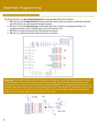
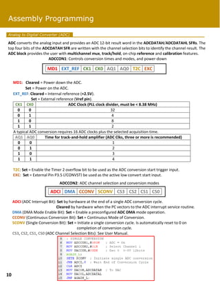
this ppt only for beginner who want to understand concept of Timer counter operation of LPC2148 step by step.
hope it may help u.
always welcoming ur suggestion.
this ppt only for beginner who want to understand concept of Timer counter operation of LPC2148 step by step.
hope it may help u.
always welcoming ur suggestion.
The Universal Asynchronous Receiver/Transmitter (UART) controller is the key component of the serial communications subsystem of a computer. The UART takes bytes of data and transmits the individual bits in a sequential fashion. At the destination, a second UART re-assembles the bits into complete bytes.
This Book helps the bargainer to getting started with avr studio and avr Micro controller interfacing. This book covers Navigating the AVR studio and many more avr interfacing examples
Electronic voting machine using mcu 89s52Saurav Kumar
Electronic voting machine using micro controller 89S52 series of 8051. this project include software code for EVM. this describe the components requirement in evm and also most importantly its working.
1 PageAlarm Clock Design Using PIC18F45E.docxmercysuttle
1 | Page
Alarm Clock Design Using PIC18F45
ELEC 310
Submitted by: Maria AlKadhem
Contents
Detailed Specification: 2
Input: 2
LCD display: 2
Microcontroller: 4
Clocking Choice 5
Working theory: 5
Pin out of the device: 6
LCD interfacing: 6
Final comments: 7
Introduction:
The major purpose of the project is to get familiar with the PIC18FXX series microcontrollers. We are ought to design an alarm clock which will be able to display the time on an LCD as well as we can give input through the dip switches. The dip switches will be able to increment the hours and minutes. We will go through the detailed design a bit later in the document.
In order to implement the alarm clock we had to make external circuitry as well which was necessary for the following functions.
· Input
· Buzzer
· Display at LCD.
The pith of the alarm clock is to run the clock of MCU in counter mode. When the counter is set the MCU starts counting till the number and then when the threshold is generated the output signal is used to start a buzzer. At the same time there is an LCD used in the circuit which will be responsible for displaying the three things.
· Current time.
· Alarm time
· Remaining time.
For setting the alarm there are two DIP switches. One for adjusting the hours and other is used for adjusting the minutes. For clearing the alarm we simply will be pressing both at a time. The corresponding ports of the MCU will be used in the INPUT mode.Detailed Specification:
Let’s discuss the detailed specifications of this device.Input:
The input of the alarm clock consists of two DIP switches. One switch will be used for adjusting the hours. The second switch will be used for the adjustment of the minutes.
Each time a button is at high logic there will be an increase in the corresponding variable of alarm.
When both of the buttons are pressed there will be a reset of clock making the value to 0.0. It will be the off state of the clock as well.LCD display:
We are using a 16x 2 display screen which is of 16 pin. The device is TRULY LCD MODULE MTC-C162DPRN-2N. It is capable of displaying 16 characters in 2 lines at a time. Making overall 32 characters.
The pin Details are given below for the LCD module.
Pin NO. Symbol Level Description
1 VSS 0V Ground
2 VDD 5.0V Supply voltage for logic
3 VO --- Input voltage for LCD
4 RS H/L H : Data, L : Instruction code
5 R/W H/L H : Read mode, L : Write mode
6 E H, H →L Chip enable signal
7 DB0 H/L Data bit 0
8 DB1 H/L Data bit 1
9 DB2 H/L Data bit 2
10 DB3 H/L Data bit 3
11 DB4 H/L Data bit 4
12 DB5 H/L Data bit 5
13 DB6 H/L Data bit 6
14 DB7 H/L Data bit 7
15 NC --- No Connection
16 NC --- No Connection
The VSS is kept at ground.
Last 2 pins are not included in the design they are not used at all.
Microcontroller:
The selected microcontroller is PIC18F452 because of the following reasons.
This powerful 10 MIPS (100 nanosecond instruction execution) yet easy-to-program (only 77 single word instructio ...
The AT89C4051 is a low-voltage, high-performance CMOS 8-bit microcontroller with
4K bytes of Flash programmable and erasable read-only memory. The device is manufactured
using Atmel’s high-density nonvolatile memory technology and is
compatible with the industry-standard MCS-51 instruction set. By combining a versatile
8-bit CPU with Flash on a monolithic chip, the Atmel AT89C4051 is a powerful
microcontroller which provides a highly-flexible and cost-effective solution to many
embedded control applications.
The AT89C4051 provides the following standard features: 4K bytes of Flash,
128 bytes of RAM, 15 I/O lines, two 16-bit timer/counters, a five-vector, two-level interrupt
architecture, a full duplex serial port, a precision analog comparator, on-chip
oscillator and clock circuitry. In addition, the AT89C4051 is designed with static logic
for operation down to zero frequency and supports two software-selectable power
saving modes. The Idle Mode stops the CPU while allowing the RAM, timer/counters,
serial port and interrupt system to continue functioning. The power-down mode saves
the RAM contents but freezes the oscillator disabling all other chip functions until the
next hardware reset.
Advanced Embedded Automatic Car Parking Systemtheijes
The International Journal of Engineering & Science is aimed at providing a platform for researchers, engineers, scientists, or educators to publish their original research results, to exchange new ideas, to disseminate information in innovative designs, engineering experiences and technological skills. It is also the Journal's objective to promote engineering and technology education. All papers submitted to the Journal will be blind peer-reviewed. Only original articles will be published.
The Art of the Pitch: WordPress Relationships and SalesLaura Byrne
Clients don’t know what they don’t know. What web solutions are right for them? How does WordPress come into the picture? How do you make sure you understand scope and timeline? What do you do if sometime changes?
All these questions and more will be explored as we talk about matching clients’ needs with what your agency offers without pulling teeth or pulling your hair out. Practical tips, and strategies for successful relationship building that leads to closing the deal.
Dev Dives: Train smarter, not harder – active learning and UiPath LLMs for do...UiPathCommunity
💥 Speed, accuracy, and scaling – discover the superpowers of GenAI in action with UiPath Document Understanding and Communications Mining™:
See how to accelerate model training and optimize model performance with active learning
Learn about the latest enhancements to out-of-the-box document processing – with little to no training required
Get an exclusive demo of the new family of UiPath LLMs – GenAI models specialized for processing different types of documents and messages
This is a hands-on session specifically designed for automation developers and AI enthusiasts seeking to enhance their knowledge in leveraging the latest intelligent document processing capabilities offered by UiPath.
Speakers:
👨🏫 Andras Palfi, Senior Product Manager, UiPath
👩🏫 Lenka Dulovicova, Product Program Manager, UiPath
Slack (or Teams) Automation for Bonterra Impact Management (fka Social Soluti...Jeffrey Haguewood
Sidekick Solutions uses Bonterra Impact Management (fka Social Solutions Apricot) and automation solutions to integrate data for business workflows.
We believe integration and automation are essential to user experience and the promise of efficient work through technology. Automation is the critical ingredient to realizing that full vision. We develop integration products and services for Bonterra Case Management software to support the deployment of automations for a variety of use cases.
This video focuses on the notifications, alerts, and approval requests using Slack for Bonterra Impact Management. The solutions covered in this webinar can also be deployed for Microsoft Teams.
Interested in deploying notification automations for Bonterra Impact Management? Contact us at sales@sidekicksolutionsllc.com to discuss next steps.
Smart TV Buyer Insights Survey 2024 by 91mobiles.pdf91mobiles
91mobiles recently conducted a Smart TV Buyer Insights Survey in which we asked over 3,000 respondents about the TV they own, aspects they look at on a new TV, and their TV buying preferences.
Essentials of Automations: Optimizing FME Workflows with ParametersSafe Software
Are you looking to streamline your workflows and boost your projects’ efficiency? Do you find yourself searching for ways to add flexibility and control over your FME workflows? If so, you’re in the right place.
Join us for an insightful dive into the world of FME parameters, a critical element in optimizing workflow efficiency. This webinar marks the beginning of our three-part “Essentials of Automation” series. This first webinar is designed to equip you with the knowledge and skills to utilize parameters effectively: enhancing the flexibility, maintainability, and user control of your FME projects.
Here’s what you’ll gain:
- Essentials of FME Parameters: Understand the pivotal role of parameters, including Reader/Writer, Transformer, User, and FME Flow categories. Discover how they are the key to unlocking automation and optimization within your workflows.
- Practical Applications in FME Form: Delve into key user parameter types including choice, connections, and file URLs. Allow users to control how a workflow runs, making your workflows more reusable. Learn to import values and deliver the best user experience for your workflows while enhancing accuracy.
- Optimization Strategies in FME Flow: Explore the creation and strategic deployment of parameters in FME Flow, including the use of deployment and geometry parameters, to maximize workflow efficiency.
- Pro Tips for Success: Gain insights on parameterizing connections and leveraging new features like Conditional Visibility for clarity and simplicity.
We’ll wrap up with a glimpse into future webinars, followed by a Q&A session to address your specific questions surrounding this topic.
Don’t miss this opportunity to elevate your FME expertise and drive your projects to new heights of efficiency.
Kubernetes & AI - Beauty and the Beast !?! @KCD Istanbul 2024Tobias Schneck
As AI technology is pushing into IT I was wondering myself, as an “infrastructure container kubernetes guy”, how get this fancy AI technology get managed from an infrastructure operational view? Is it possible to apply our lovely cloud native principals as well? What benefit’s both technologies could bring to each other?
Let me take this questions and provide you a short journey through existing deployment models and use cases for AI software. On practical examples, we discuss what cloud/on-premise strategy we may need for applying it to our own infrastructure to get it to work from an enterprise perspective. I want to give an overview about infrastructure requirements and technologies, what could be beneficial or limiting your AI use cases in an enterprise environment. An interactive Demo will give you some insides, what approaches I got already working for real.
Software Delivery At the Speed of AI: Inflectra Invests In AI-Powered QualityInflectra
In this insightful webinar, Inflectra explores how artificial intelligence (AI) is transforming software development and testing. Discover how AI-powered tools are revolutionizing every stage of the software development lifecycle (SDLC), from design and prototyping to testing, deployment, and monitoring.
Learn about:
• The Future of Testing: How AI is shifting testing towards verification, analysis, and higher-level skills, while reducing repetitive tasks.
• Test Automation: How AI-powered test case generation, optimization, and self-healing tests are making testing more efficient and effective.
• Visual Testing: Explore the emerging capabilities of AI in visual testing and how it's set to revolutionize UI verification.
• Inflectra's AI Solutions: See demonstrations of Inflectra's cutting-edge AI tools like the ChatGPT plugin and Azure Open AI platform, designed to streamline your testing process.
Whether you're a developer, tester, or QA professional, this webinar will give you valuable insights into how AI is shaping the future of software delivery.
Key Trends Shaping the Future of Infrastructure.pdfCheryl Hung
Keynote at DIGIT West Expo, Glasgow on 29 May 2024.
Cheryl Hung, ochery.com
Sr Director, Infrastructure Ecosystem, Arm.
The key trends across hardware, cloud and open-source; exploring how these areas are likely to mature and develop over the short and long-term, and then considering how organisations can position themselves to adapt and thrive.
Key Trends Shaping the Future of Infrastructure.pdf
Assembly programming II
1. Chapter 3
Assembly
Programming II
Peripherals on Microcontrollers are its means of communicating with the external world and
execute some special tasks, the most commons are: Parallel Input-Output Ports (P0-3), ADC, DAC,
PWM, SPI, I2C, Timers/Counters, UART, Voltage Reference, PLL, SFR, Dual Data Pointers, Power
Supply Monitor, Watchdog Timer, Time Interval Counter, among others
2. Assembly Programming………………….…………….…….………. 1
General Purpose Input-Output Ports (P03)…….…………………..……1
Phase Lock Loop (PLL).………..…..………………………………….2
Timers/Counters.………..………..…………………………………2
Digital to Analog Converters (DAC).……………………...…………….5
Pulse-Width Modulator (PWM).……………………...……………….8
Analog to Digital Converters (ADC).…………………….....…………10
UART Serial Interface.…………………….………….....…………12
3. The Microconverter uses four input/output ports to exchange data with external devices:
✓ P0: Port 0 is an 8-Bit Open-Drain Bidirectional I/O Port, external pull-up resistors are therefore required
when Port 0 pins are used as general-purpose outputs.
✓ P1: Port 1 is an 8-bit input port only. Unlike other ports, Port 1 defaults to Analog Input Mode. To
configure any Port 1 pin as a Digital Input, write a 0 to the Port 1 bit.
✓ P2: Port 2 is a bidirectional port with internal pull-up resistors.
✓ P3: Port 3 is a bidirectional port with internal pull-up resistors.
Open Drain: A transistor connects to low and nothing else. Open drain is useful when multiple gates or pins are
connected together with an external pull-up. If all the pins are high, they are all open circuits and the pull-up
drives the pins high. If any pin is low they all go low as they tied together. This configuration effectively forms an
AND gate. Open drain output circuits must be complemented with a “Pull-Up-Resistor” to function properly. The
open drain commonly used to drive devices such as Relays or Motors which require higher operating voltages
than the usual 5-volt logic supply. Below, connection of 12V Relay.
General Purpose Input-Output Ports (P0-3)
Assembly Programming
P0
P2
P3
P1
1
4. The ADuC842 are intended for use with a 32.768 kHz watch crystal. A PLL locks onto a multiple (512) of this to
provide a stable 16.777216 MHz clock for the system. The default core clock is the PLL clock divided by 8 or
2.097152 MHz. The core clock can be changed changing the CD bits in PLLCON (PLL control register)
The maximum core clock (16.777216 MHz) can be obtained with PLLCON = 40H
The Timer/Counter is a 16-bit register. Each timer/counter consists of two 8-bit registers: THx and TLx (x = 0, 1, and 2).
All three can be configured to operate in one of two modes:
✓ Timers: The TLx register is incremented every core clock period. Thus, one can think of it as counting clock
periods.
✓ Counters: The TLx register is incremented by a 1-to-0 transition at its corresponding external input pin: T0, T1,
or T2.
User configuration and control of all timer operating modes is achieved via three SFRs:
TMOD: Configuration for Timers 0 and 1
GATE: “0” enable Timer/Controlx when /INTx pin is high and TRx is set (x = 0 and 1)
“1” enable Timer/Controlx TRx is set (x = 0 and 1)
C/T: “0” select timer operation (input from internal system clock)
“1” select counter operation, input from Tx pin (x = 0 and 1)
M1, M0: Timer Mode Select
0 0: THx operates as an 8-bit timer/counter. TLx serves as 5-bit prescaler
0 1: 16-Bit Timer/Counter. THx and TLx are cascaded; there is no prescaler.
1 0: 8-Bit Autoreload Timer/Counter. THx holds a value that is to be reloaded into TLx each time it overflows
1 1: See User Manual
Phase Lock Loop (PLL)
Timers/Counters
Assembly Programming
0 1 0 0 0 CD2 CD1 CD0
16.777216 MHz 0 0 0
8.388608 MHz 0 0 1
4.194304 MHz 0 1 0
2.097152 MHz 0 1 1
1.048576 MHz 1 0 0
0.524288 MHz 1 0 1
0.262144 MHz 1 1 0
0.131072 1 1 1
T/C 1 T/C 0
GATE C/T M1 M0 GATE C/T M1 M0
2
5. TCON: Control for timers 0 and 1
TFx: Cleared by hardware when the PC vectors to the ISR
Set by hardware on a Timer/Counter x overflow (x = 0 and 1)
TRx: Cleared by the user to turn off Timer/Counter x.
Set by the user to turn on Timer/Counter x.
NU: These bits are not used in the control of Timer/Counter 0 and 1. Used for control of external interrupts pins.
T2CON: Timer/Counter 2 Control Register
TF2: Cleared by user software.
Set by hardware on a Timer/Counter 2 overflow.
EXF2: Cleared by user software.
Set by hardware when a reload/capture is caused by a negative transition on T2EX and EXEN2 = 1.
RCLK: Set by the user to enable the serial port.
Cleared by the user to enable Timer 1 overflow to be used for the receive clock.
TCLK: Set by the user to enable the serial port.
Cleared by the user to enable Timer 1 overflow to be used for the transmit clock.
EXEN2: Set by the user to enable a capture or reload to occur as result of a negative transition on T2EX.
Cleared by the user for Timer 2 to ignore events at T2EX.
TR2: Set by the user to start Timer 2.
Cleared by the user to stop Timer 2.
CNT2: Set by the user to select counter function (input from external T2 pin).
Cleared by the user to select timer function (input from on-chip core clock).
CAP2: Set by the user to enable captures on negative transitions at T2EX if EXEN2 = 1.
Cleared by the user to enable auto reloads with Timer 2 overflows or negative transitions at T2EX.
To compute the values of 16-bit timer/ counters (THx and TLx, x = 0, 1 and 2), can be used:
Timer: THxTLx = 65536 – Tdes*Fclk
where: Tdes = Desired interrupt time (sec)
Fclk = Frequency of core clock (Hz, defined in PLLCON)
Example: Tdes = 1msec; 16777216 Hz THxTLx = 48759 BE77H
Counter: THxTLx = 65536 – N
where: N =Number of 1-to-0 transition in Tx (x = 0, 1 and 2)
Example: N = 5 transitions (2msec/transition) THxTLx = 65531 FFFBH (Interrupt/10msec)
The next program tests the Timer/Counters
Assembly Programming
T/C 1 T/C 0
TF1 TR1 TF0 TR0 NU NU NU NU
TF2 EXF2 RCLK TCLK EXEN2 TR2 CNT2 CAP2
3
7. The Microconverter incorporates two 12-bit voltage output DACs on chip. Each has two selectable ranges, 0 V to
VREF (internal 2.5 V reference) and 0 V to AVDD. Both DACs share a control register, DACCON, and four data
registers, DAC1H, DAC1L, DAC0H, and DAC0L.
DACCON: DAC Control Register
Mode: Cleared = 12-bit mode.
Set = 8-bit mode (write eight bits to DACxL SFR, x = 0 and 1).
RNG1: Cleared = DAC1 range 0V − VREF.
Set = DAC1 range 0V − AVDD.
RNG0: Set = DAC0 range 0V − AVDD.
Cleared = DAC0 range 0V − VREF.
CLR1: Set = DAC1 output normal.
Cleared = DAC1 output forced to 0 V.
CLR0: Set = DAC0 output normal.
Cleared = DAC0 output forced to 0 V.
SYNC: Set = DAC outputs update as soon as DACxL SFRs are written.
Cleared = User can simultaneously update both DACs.
PD1: Set = power on DAC1.
Cleared = power off DAC1.
PD0: Set = power on DAC0.
Cleared = power off DAC0.
Timer/Counter 1: Counter, 5 transitions 1-0 (2msec) in T1 (Output: P2.1)
Timer/Counter 0: Timer 16 bits, 1msec, Counter: 200 (Output: P2.0)
Digital to Analog Converters (DAC)
Assembly Programming
Mode RNG1 RNG0 CLR1 CLR0 SYNC PD1 PD0
5
8. The following program compute the codes that generates a sinusoidal function
Assembly Programming
6
9. After Reset, the CFG842 register is 00H, then the DAC output buffer is active. The example of assembler program,
using DAC1 as sine generator is shows below
7
Assembly Programming
10. The PWM uses five SFRs: PWMCON, controls the different modes of operation of the PWM as well as the PWM
clock frequency. PWM0H/L and PWM1H/L are the data registers that determine the duty cycles. The output pins
that the PWM uses are determined by the CFG842 register, and can be either P2.6 and P2.7 or P3.4 and P3.3.
PWMCON: PWM Control Register
The output of sine generator is shows below
Output at DAC1
Pulse-Width Modulator (PWM)
8
SNGL MD2 MD1 MD0 CDIV1 CDIV0 CSEL1 CSEL0
Assembly Programming
SNGL: SET = Turns off PMW output at P2.6 or P3.4
MD2 MD1 MD0 Mode
0 0 0 PWM Disabled
0 0 1 Single variable resolution PWM on P2.7 or P3.3
0 1 0 Twin 8-bit PWM
0 1 1 Twin 16-bit PWM
1 0 0 Dual NRZ 16-bit ∑-∆ DAC
1 0 1 Dual 8-bit PWM
1 1 0 Dual RZ 16-bit ∑-∆ DAC
1 1 1 Reserved
CDIV1 CDIV0 Clock divider
0 0 Selected Clock/1
0 1 Selected Clock/4
1 0 Selected Clock/16
1 1 Selected Clock/64
11. To compute the values of 16-bit data registers PWM0H/L and PWM1H/L in mode 1:
Frequency: PWM1H/L = Fclk / Fdes
where: Fdes = Desired frequency (Hz)
Fclk = Frequency of clock source
Duty Cycle: PWM0H/L = Fclk / ((100/DC)*Fdes)
where: Fdes = Desired frequency (Hz)
Fclk = Frequency of clock source
DC = Duty Cycle
Example: Fdes = 1KHz; DC = 50%; Fclk = 16777216 Hz
PWM1H/L = 16777216 / 1000 16777 4189H PWM1H = 41H, PWM1L = 89H
PWM0H/L = 16777216 / ((100/50)*1000) 8388 20C4H PWM0H = 20H, PWM0L = C4H
Output at PWM1 (P2.7)
Assembly Programming
CSEL1 CSEL0 Clock Source
0 0 fXTAL/15
0 1 fXTAL
1 0 External input at P3.4/T0
1 1 fVCO = 16777216 Hz
9
Assembly Programming
12. ADC converts the analog input and provides an ADC 12-bit result word in the ADCDATAH/ADCDATAHL SFRs. The
top four bits of the ADCDATAH SFR are written with the channel selection bits to identify the channel result. The
ADC block provides the user with multichannel mux, track/hold, on-chip reference and calibration features.
ADCCON1: Controls conversion times and modes, and power-down
MD1 EXT_REF CK1 CK0 AQ1 AQ0 T2C EXC
ADCCON2: ADC channel selection and conversion modes
Analog to Digital Converter (ADC)
Assembly ProgrammingAssembly Programming
MD1: Cleared = Power down the ADC.
Set = Power on the ADC.
EXT_REF: Cleared = Internal reference (+2.5V).
Set = External reference (Vref pin).
CK1 CK0 ADC Clock (PLL clock divider, must be < 8.38 MHz)
0 0 32
0 1 4
1 0 8
1 1 2
A typical ADC conversion requires 16 ADC clocks plus the selected acquisition time.
AQ1 AQ0 Time for track-and-hold amplifier (ADC Clks, three or more is recommended)
0 0 1
0 1 2
1 0 3
1 1 4
T2C: Set = Enable the Timer 2 overflow bit to be used as the ADC conversion start trigger input.
EXC: Set = External Pin P3.5 (/CONVST) be used as the active low convert start input.
ADCI DMA CCONV SCONV CS3 CS2 CS1 CS0
ADCI (ADC Interrupt Bit): Set by hardware at the end of a single ADC conversion cycle.
Cleared by hardware when the PC vectors to the ADC interrupt service routine.
DMA (DMA Mode Enable Bit): Set = Enable a preconfigured ADC DMA mode operation.
CCONV (Continuous Conversion Bit): Set = Continuous Mode of Conversion.
SCONV (Single Conversion Bit): Set = Initiate a single conversion cycle. Is automatically reset to 0 on
completion of conversion cycle.
CS3, CS2, CS1, CS0 (ADC Channel Selection Bits): See User Manual.
10
13. ADCCON3: ADC calibration modes and busy status
Buffering the analog inputs is a good for protection of analog input and implement antialiasing filter
Assembly Programming
BUSY 0 AVGS1 AVGS0 0 RSVD TYPICAL SCAL
BUSY (ADC Busy Status Bit): Set during ADC conversion or calibration cycle
AVGS1 AVGS0 ADC readings that are averaged during a calibration cycle
0 0 15
0 1 1
1 0 31
1 1 63
RSVD: Set by user when performing calibration.
TYPICAL: Set = Gain Calibration.
Clear = Offset Calibration
SCAL: Set = Start the selected calibration cycle
Cleared when the calibration cycle is completed
11
14. The following program shows how to implement the UART communication, was tested with Tera Term
UART Serial Interface
Assembly Programming
12