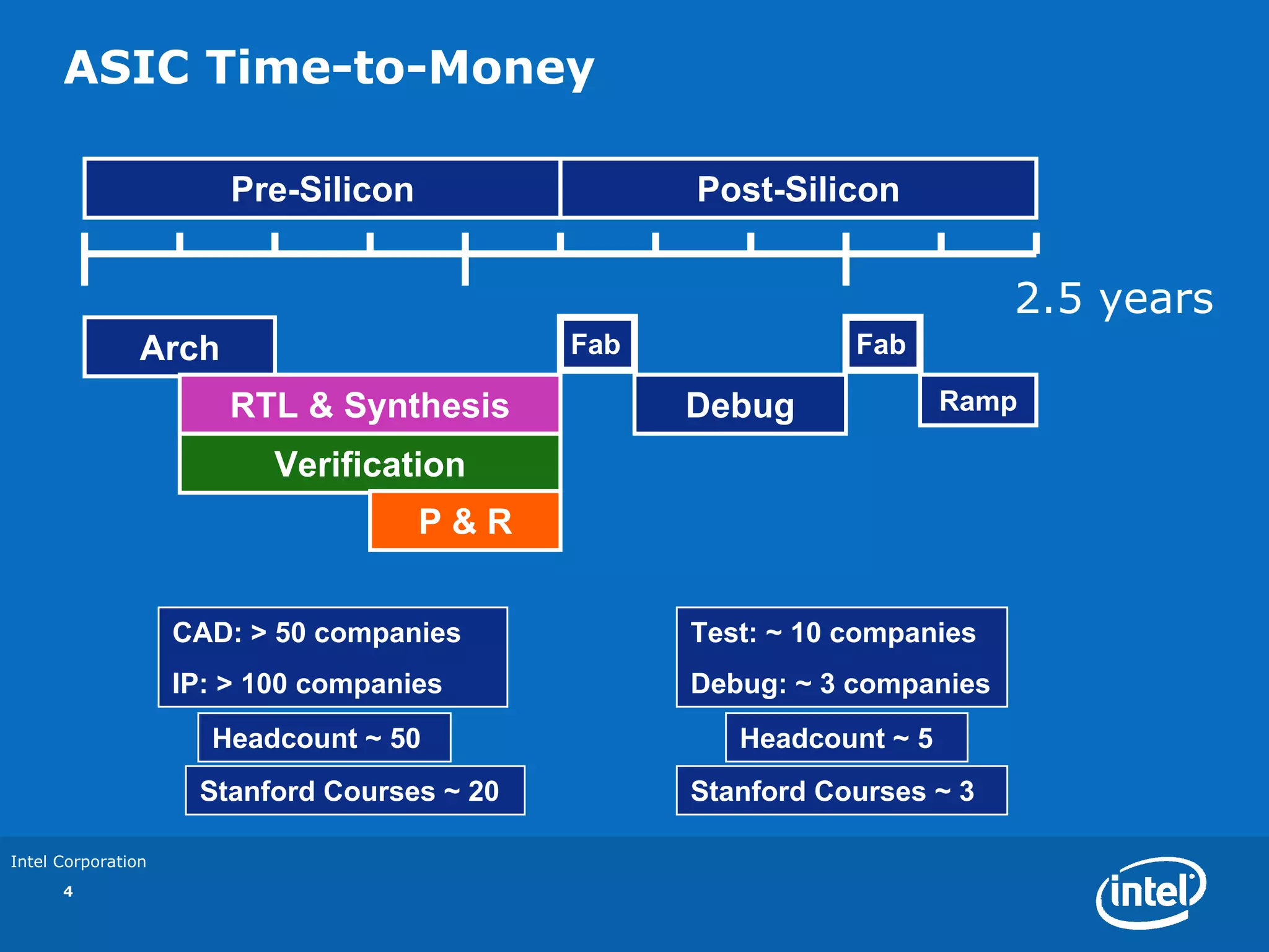
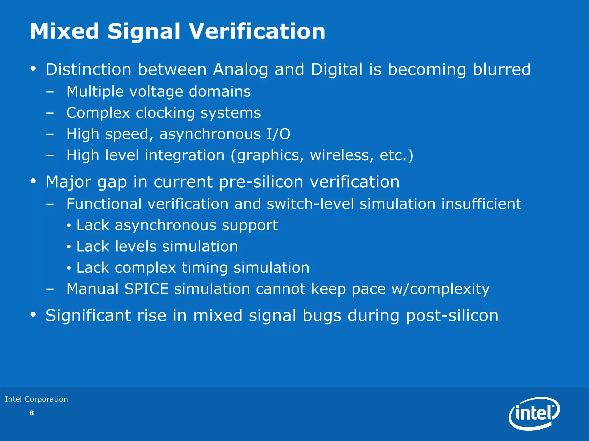
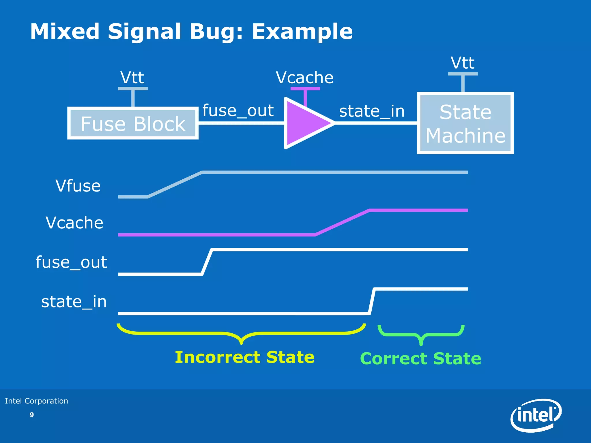
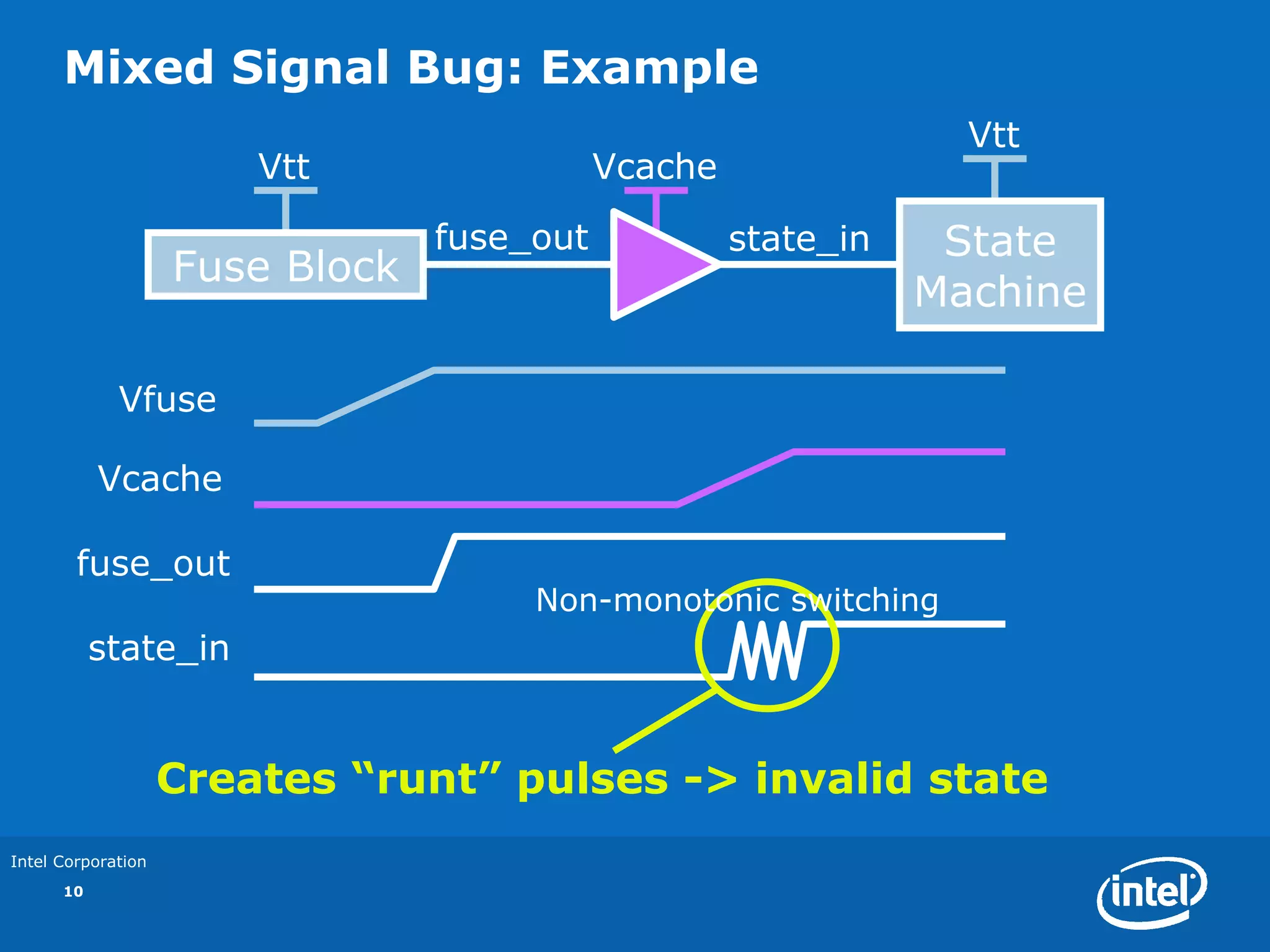
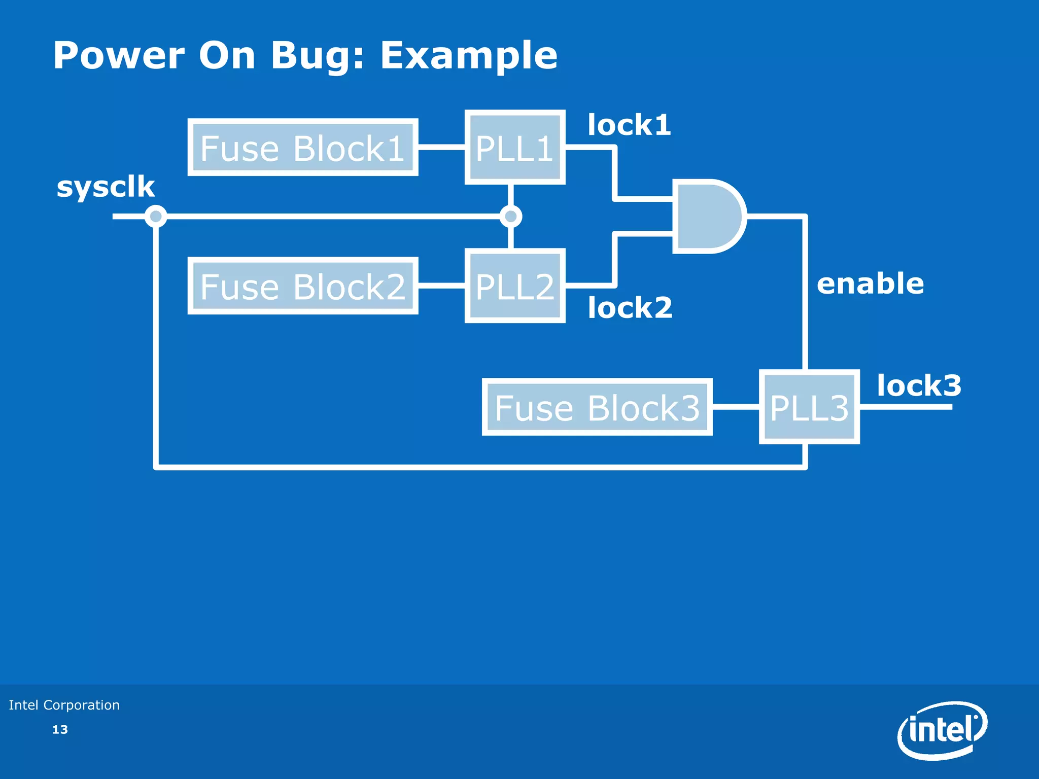
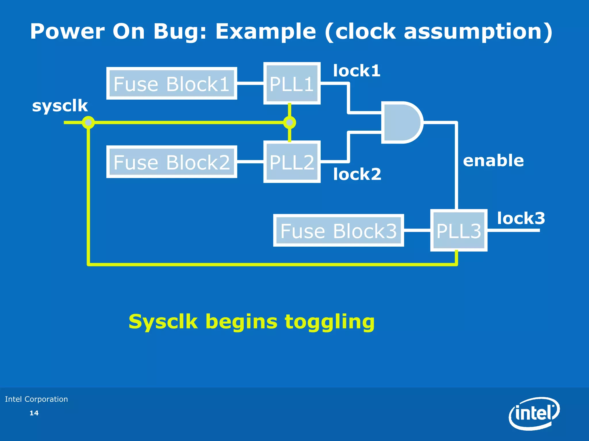
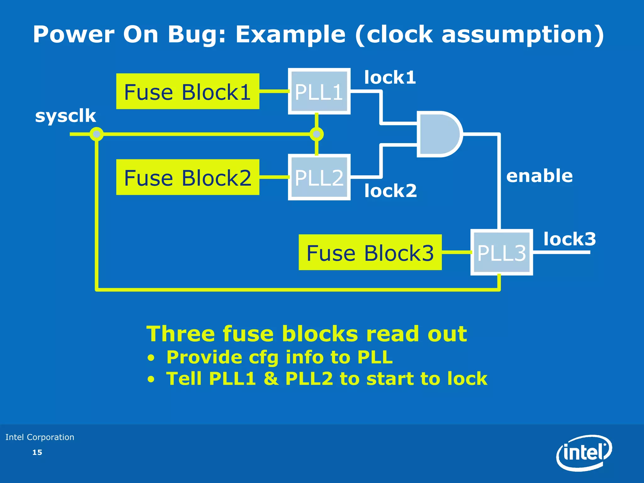
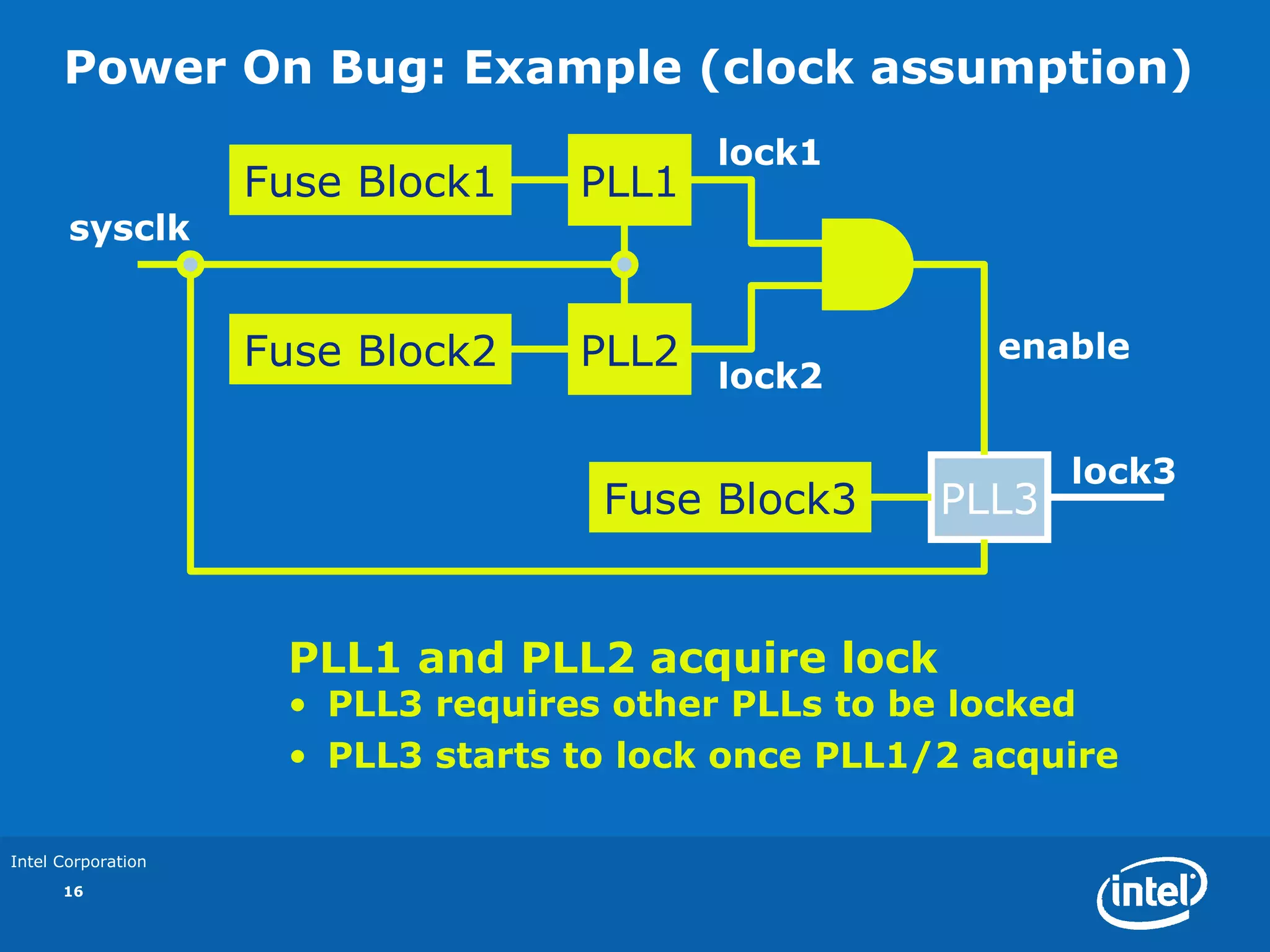
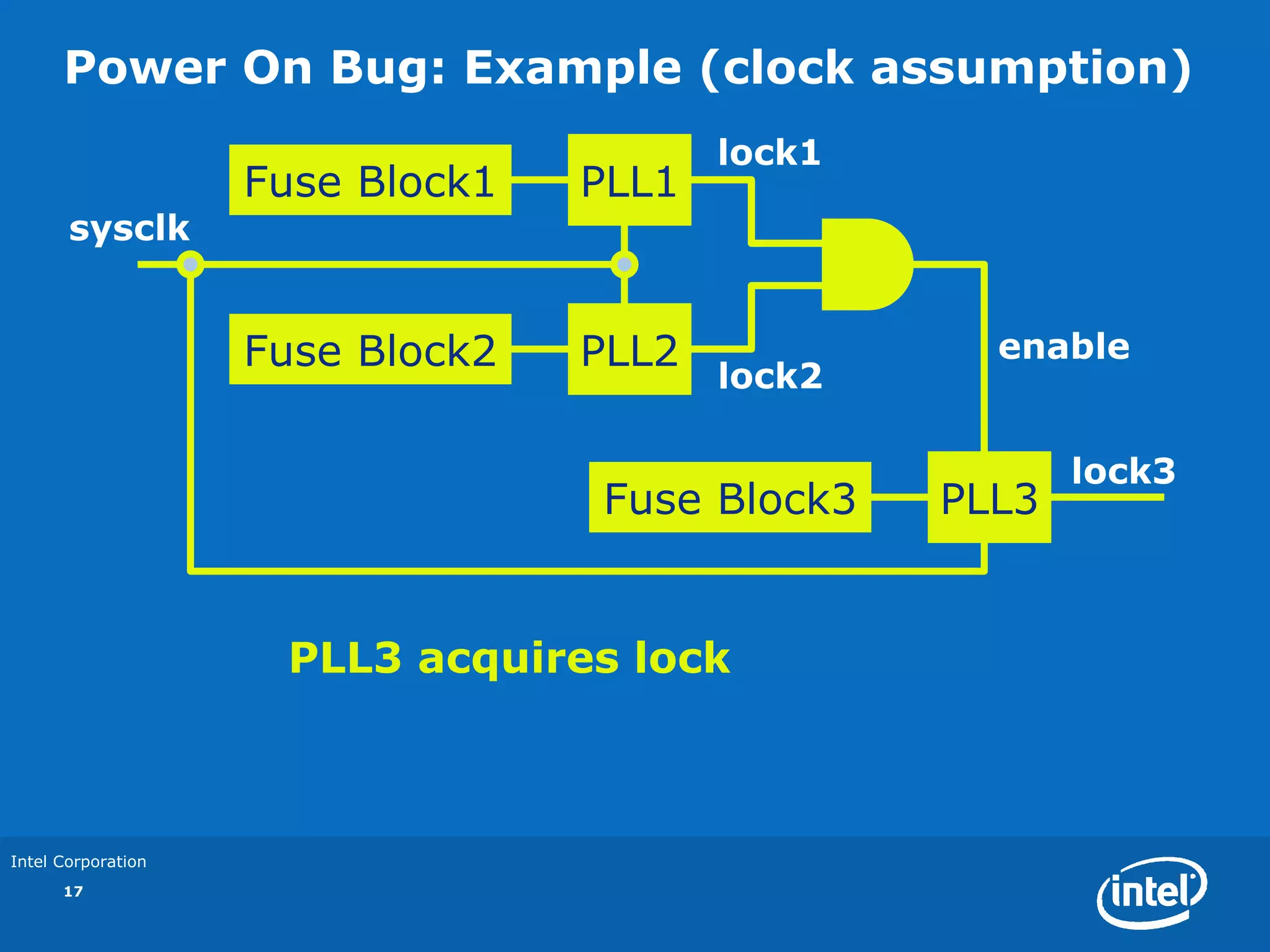
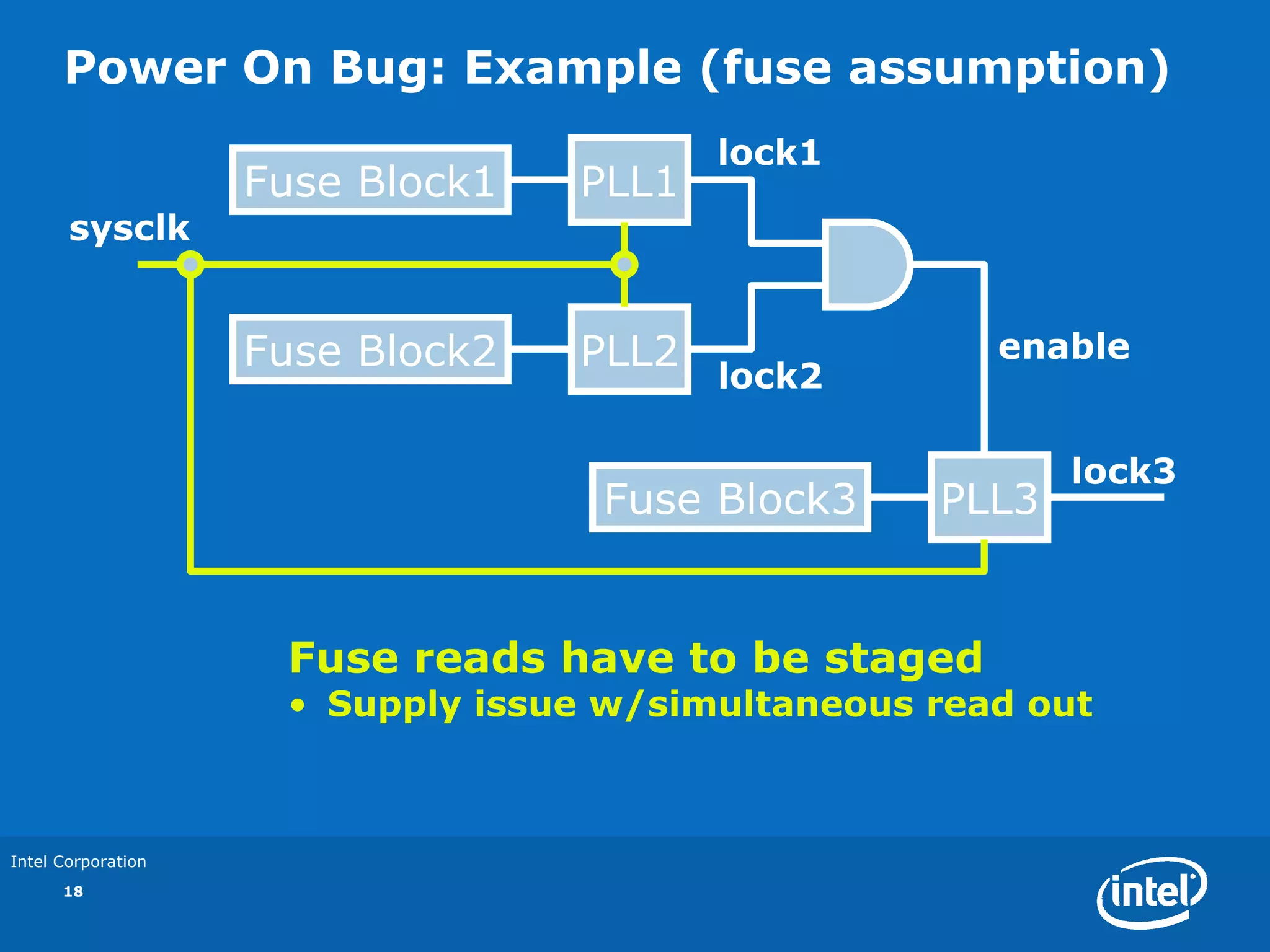
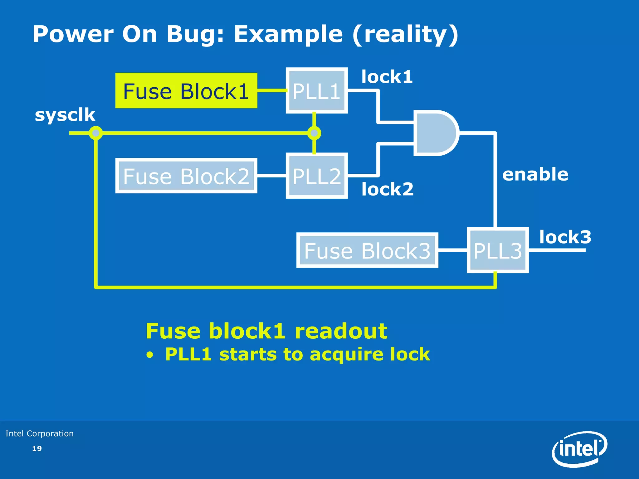
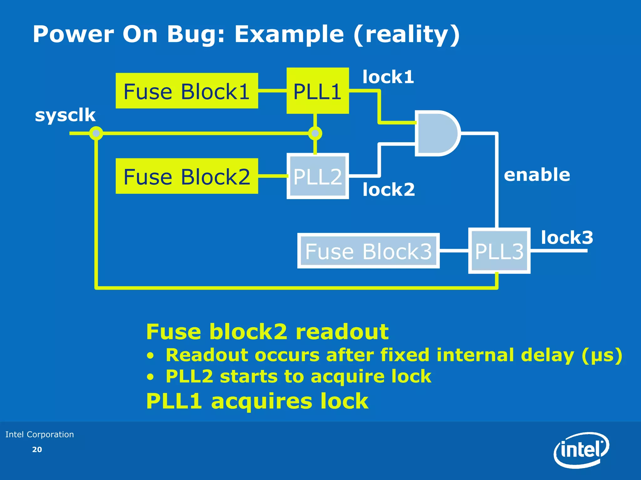
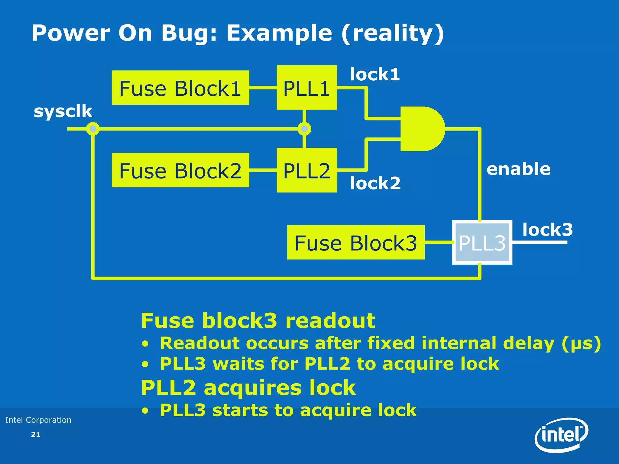
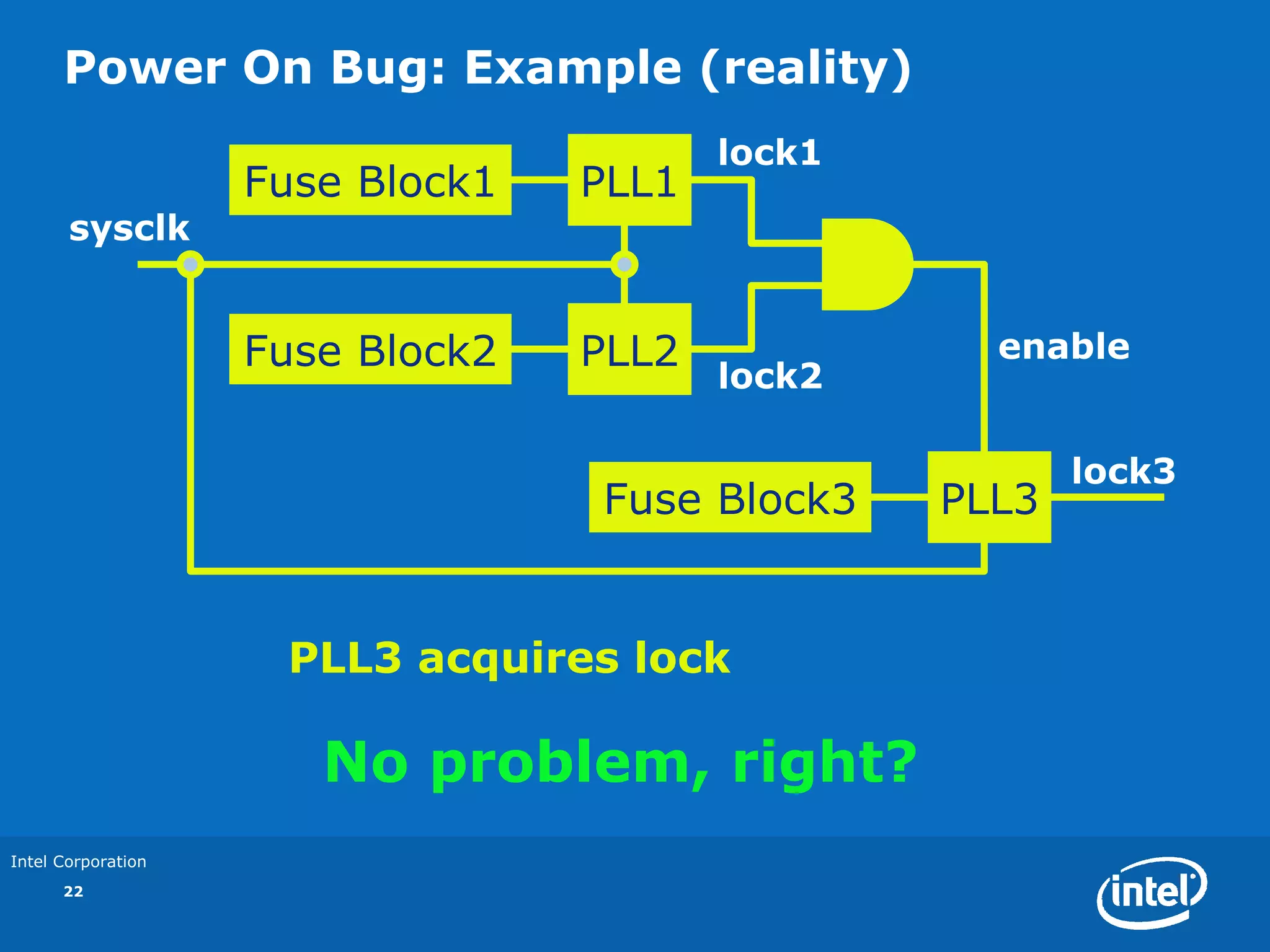
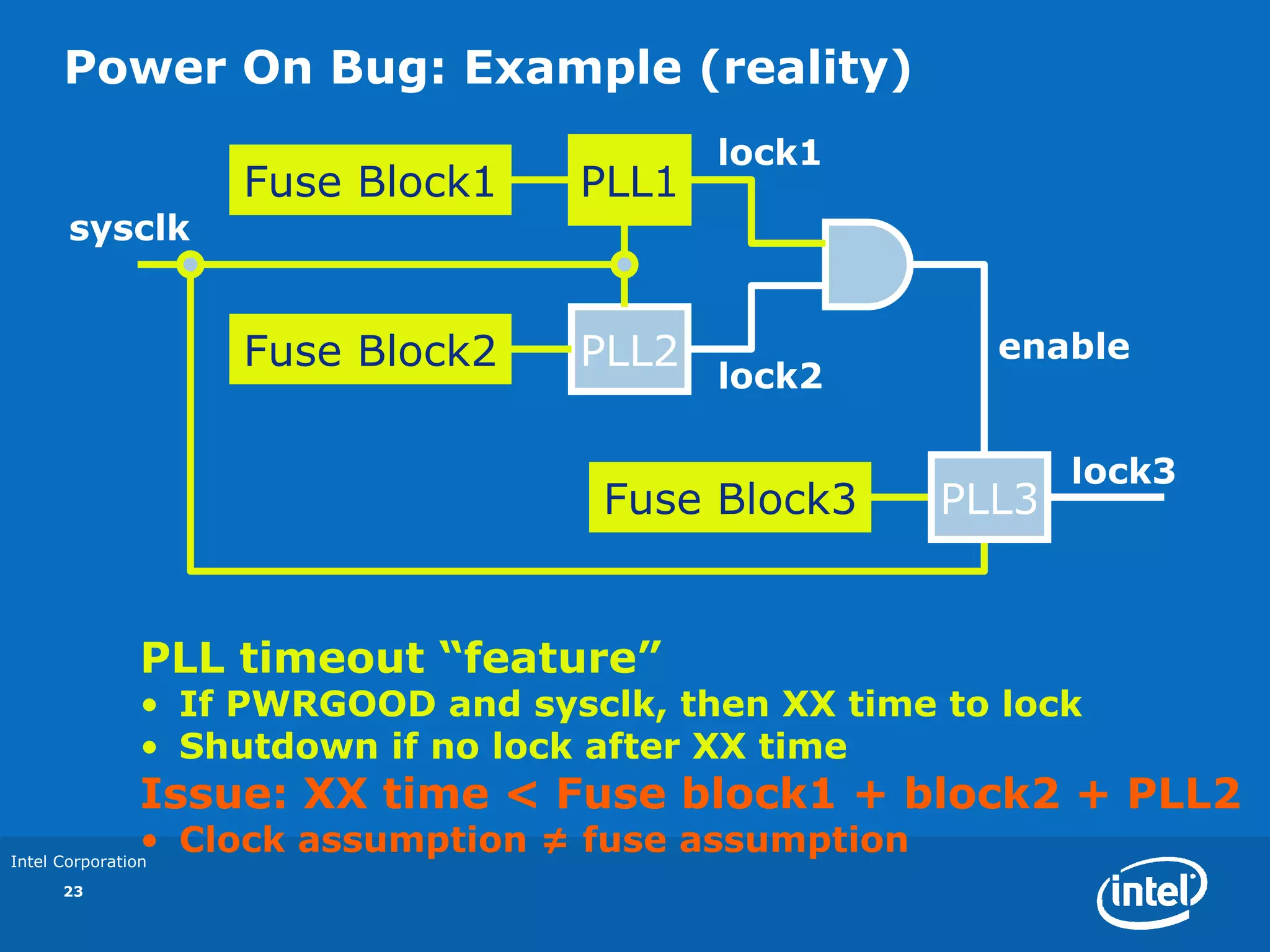
Pre-Si Verification for Post-Si Validation

                                      Jason Stinson
                                  Principal Engineer
                  Enterprise Microprocessor Division
                                   Intel Corporation

                                   Dec 5th, 2006
Overview


Intel Corporation
      2
Post-Silicon Validation
      •   Increasingly larger percentage of time-to-money
          – Design advances result in flattening/shrinking schedules
            • Better design tools/methodologies
            • More focus on integration vs. creation
          – Post-Si Validation schedules continue to grow
            • Low investment in tools/methodologies
            • Complexity driven by design size not design “source”
            • Multiple SKUs effectively create multiple validation cycles


Intel Corporation
      3
ASIC Time-to-Money

                        Pre-Silicon                Post-Silicon


                                                                          2.5 years
                Arch                         Fab              Fab

                        RTL & Synthesis            Debug              Ramp

                           Verification
                                      P&R


                    CAD: > 50 companies            Test: ~ 10 companies
                    IP: > 100 companies            Debug: ~ 3 companies
                      Headcount ~ 50                  Headcount ~ 5
                     Stanford Courses ~ 20         Stanford Courses ~ 3

Intel Corporation
      4
Post-Silicon Validation (cont’d)
      •   Industry starting to make larger post-Si investments
          – Growing EDA industry (DFx insertion, content generation, etc)
          – Greater design investment in post-Si feature sets
          – Increase in academic interest/research (slow)
      •   Two largest VLSI challenges: Verification and Validation
          – Verification = Pre-silicon verification of design thru simulation
          – Validation = Post-silicon validation of design thru silicon testing
          – Design is no longer the most difficult issue


Intel Corporation
      5
How does Verification affect Validation?
      •   Pre-Si verification = Post-Si validation
          – Same goal: find the bugs, debug ‘em, fix ‘em
      •   Verification needs to:
          – Move beyond functional verification
            • Although still complex, not the biggest challenge
          – Own mixed-signal verification
            • Interaction of complex electrical effects is huge challenge
          – Enable faster post-Si validation
            • Validate functional & mixed-signal power on and reset
            • Verify design-for-silicon feature set functionality
          – Provide better Silicon functional content
            • Electrical validation requires functional content


Intel Corporation
      6
Focus Areas
      •   Mixed Signal Verification
      •   Power on/Reset Verification
      •   DFx Verification


Intel Corporation
      7
Mixed Signal Verification
      •   Distinction between Analog and Digital is becoming blurred
          –     Multiple voltage domains
          –     Complex clocking systems
          –     High speed, asynchronous I/O
          –     High level integration (graphics, wireless, etc.)
      •   Major gap in current pre-silicon verification
          – Functional verification and switch-level simulation insufficient
            • Lack asynchronous support
            • Lack levels simulation
            • Lack complex timing simulation
          – Manual SPICE simulation cannot keep pace w/complexity
      •   Significant rise in mixed signal bugs during post-silicon


Intel Corporation
      8
Mixed Signal Bug: Example
                                                                  Vtt
                       Vtt                  Vcache

                                 fuse_out            state_in    State
                    Fuse Block
                                                                Machine

             Vfuse

           Vcache

          fuse_out

          state_in


                             Incorrect State           Correct State

Intel Corporation
      9
Mixed Signal Bug: Example
                                                                  Vtt
                        Vtt                 Vcache

                                 fuse_out            state_in    State
                    Fuse Block
                                                                Machine

             Vfuse

           Vcache

        fuse_out
                                      Non-monotonic switching
           state_in


                    Creates “runt” pulses -> invalid state
Intel Corporation
      10
Mixed Signal Bug Conclusions
      •    Functional verification and switch-level simulation insufficient
           – No supply ramp transition (0 -> 1)
           – No analog understanding of ramp (metastable transition)
      •    Manual simulation or Electrical Rules checking could catch
           – Requires fullchip visibility and power on understanding
      •    Mixed signal verification
           – Formal extraction of critical power on circuitry & known analog
             interactions
           – Basic SPICE engine combined with functional vector stimulus


Intel Corporation
      11
Power On/Reset Verification
      •    Complexity of power on and reset increasing
           – More state to reset = more interactions
           – Assumptions are often invalid (mutex, DC, valid state, etc)
           – Analog components factor significantly
             • Emphasizing need for greater mixed signal verification
           – Unknown IP block interactions
      •    Traditionally treated as lower verification priority
           – Old mantra: “Gate with PWRGOOD and route RESET to all state”
             • Eliminated need for significant (any) pre-silicon verification
           – New mantra: “Formally verify power on and reset”
             • Costly to get power on/reset signals to all blocks
             • Complexity of system no longer ensure valid bring up


Intel Corporation
      12
Power On Bug: Example
                                         lock1
                    Fuse Block1   PLL1
       sysclk


                    Fuse Block2   PLL2             enable
                                         lock2

                                                        lock3
                                  Fuse Block3    PLL3


Intel Corporation
      13
Power On Bug: Example (clock assumption)
                                         lock1
                    Fuse Block1   PLL1
       sysclk


                    Fuse Block2   PLL2             enable
                                         lock2

                                                        lock3
                                  Fuse Block3    PLL3


                     Sysclk begins toggling


Intel Corporation
      14
Power On Bug: Example (clock assumption)
                                           lock1
                    Fuse Block1     PLL1
       sysclk


                    Fuse Block2     PLL2                   enable
                                           lock2

                                                              lock3
                                     Fuse Block3      PLL3


                     Three fuse blocks read out
                     • Provide cfg info to PLL
                     • Tell PLL1 & PLL2 to start to lock


Intel Corporation
      15
Power On Bug: Example (clock assumption)
                                          lock1
                    Fuse Block1    PLL1
       sysclk


                    Fuse Block2    PLL2                 enable
                                          lock2

                                                            lock3
                                    Fuse Block3      PLL3


                     PLL1 and PLL2 acquire lock
                     • PLL3 requires other PLLs to be locked
                     • PLL3 starts to lock once PLL1/2 acquire

Intel Corporation
      16
Power On Bug: Example (clock assumption)
                                         lock1
                    Fuse Block1   PLL1
       sysclk


                    Fuse Block2   PLL2             enable
                                         lock2

                                                        lock3
                                  Fuse Block3    PLL3


                     PLL3 acquires lock


Intel Corporation
      17
Power On Bug: Example (fuse assumption)
                                         lock1
                    Fuse Block1   PLL1
       sysclk


                    Fuse Block2   PLL2                enable
                                         lock2

                                                          lock3
                                   Fuse Block3     PLL3


                     Fuse reads have to be staged
                     • Supply issue w/simultaneous read out


Intel Corporation
      18
Power On Bug: Example (reality)
                                          lock1
                    Fuse Block1    PLL1
       sysclk


                    Fuse Block2    PLL2                enable
                                          lock2

                                                            lock3
                                     Fuse Block3     PLL3


                     Fuse block1 readout
                     • PLL1 starts to acquire lock


Intel Corporation
      19
Power On Bug: Example (reality)
                                          lock1
                    Fuse Block1    PLL1
       sysclk


                    Fuse Block2    PLL2                 enable
                                          lock2

                                                             lock3
                                    Fuse Block3       PLL3


                     Fuse block2 readout
                     • Readout occurs after fixed internal delay (µs)
                     • PLL2 starts to acquire lock
                     PLL1 acquires lock
Intel Corporation
      20
Power On Bug: Example (reality)
                                          lock1
                    Fuse Block1    PLL1
       sysclk


                    Fuse Block2    PLL2                 enable
                                          lock2

                                                             lock3
                                     Fuse Block3      PLL3


                     Fuse block3 readout
                     • Readout occurs after fixed internal delay (µs)
                     • PLL3 waits for PLL2 to acquire lock
                     PLL2 acquires lock
Intel Corporation
                     • PLL3 starts to acquire lock
      21
Power On Bug: Example (reality)
                                         lock1
                    Fuse Block1   PLL1
       sysclk


                    Fuse Block2   PLL2             enable
                                         lock2

                                                        lock3
                                  Fuse Block3    PLL3


                     PLL3 acquires lock

                       No problem, right?
Intel Corporation
      22
Power On Bug: Example (reality)
                                            lock1
                    Fuse Block1      PLL1
       sysclk


                    Fuse Block2      PLL2                enable
                                            lock2

                                                              lock3
                                      Fuse Block3      PLL3


                PLL timeout “feature”
                • If PWRGOOD and sysclk, then XX time to lock
                • Shutdown if no lock after XX time
                Issue: XX time < Fuse block1 + block2 + PLL2
                • Clock assumption ≠ fuse assumption
Intel Corporation
      23
Power on/Reset Conclusions
      •    Bug verified with both functional verification and switch-level
           – Original verification effort “zero’d out” fuse delay elements
             • Fuses readout simultaneously in original verification
           – Low priority     low effort    poor assumptions
      •    Mixed signal verification also would have caught issue
           – Requires long simulation times
             • Fuse delay elements & PLL lock times are very long


Intel Corporation
      24
DFx Verification
      •    Design for {Manufacturability, Test, Debug, etc}
           – “Must have” features to enable low cost and rapid product ramp
           – “Must have” features to enable validation of design & platform
      •    DFx must-have feature need is increasing
           – Higher state-to-pin ratio (same pin count, more internal state)
             • More difficult to get at internal state
             • Takes longer to get at internal state
           – Design size continues to increase
             • Must test blocks in parallel to reduce test time & validation effort
             • Must enable high coverage, automated test generation
           – ATE I/O capabilities falling behind
             • Highly configurable ATE I/O cannot keep up with product I/O
      •    DFx verification is typically lowest or zero priority
           – Results in longer post-silicon schedules and/or steppings

Intel Corporation
      25
DFx Verification: Case Study
      •    Swap Core DFT Feature
           – Used on multicore microprocessor designs
           – Enables single core diagnostic vector to run on any core
             • Can be run on single core or all cores in parallel
           – Huge savings in effort and cost
             • Reduces vector generation requirements
             • Reduces core validation effort
             • Reduces test time (cores run in parallel)
      •    Two microprocessor designs
           – Both multi-core + large cache
           – Processor #1: Significant effort in SwapCore verification
           – Processor #2: Low effort in SwapCore verification


Intel Corporation
      26
DFx Verification: Case Study (cont’d)
      •    Processor #1 Experience
           – Swap core worked seamlessly with first silicon
           – Able to run single-core or cores-in-parallel
           – 80% of validation effort focused on single-core
             • Manufacturing ensured all cores matched single core validation
             • Remaining validation verified multi-core operation
           – Manufacturing test cost met all goals
      •    Processor #2 Experience
           – Swap core didn’t work completely with first silicon
             • Required effort to debug issues
             • Included fixes in next stepping
           – Swap core still broken on next stepping (onion peeling issue)
           – Impacted post-Silicon validation effort/schedule
             • Had to ensure same coverage/functionality
           – Impacted manufacturing test vector memory
             • Threatened to become test time issue

Intel Corporation
      27
Last Thoughts


Intel Corporation
      28
Last Thoughts
      •    Verification and Validation are the most critical VLSI challenge
           – Design is no longer the most difficult challenge
      •    Key post-silicon challenges
           – Schedule/effort limiting bugs
             • Power on/reset
             • Electrical bugs
               – Drives need for mixed signal verification
             • High speed I/O
           – Bug escapes
             • Comprehensive test content coverage


           Pre-Si verification has huge impact on
                       post-Si schedules
Intel Corporation
      29

Stinson post si and verification

  • 1.
    Pre-Si Verification forPost-Si Validation Jason Stinson Principal Engineer Enterprise Microprocessor Division Intel Corporation Dec 5th, 2006
  • 2.
  • 3.
    Post-Silicon Validation • Increasingly larger percentage of time-to-money – Design advances result in flattening/shrinking schedules • Better design tools/methodologies • More focus on integration vs. creation – Post-Si Validation schedules continue to grow • Low investment in tools/methodologies • Complexity driven by design size not design “source” • Multiple SKUs effectively create multiple validation cycles Intel Corporation 3
  • 4.
    ASIC Time-to-Money Pre-Silicon Post-Silicon 2.5 years Arch Fab Fab RTL & Synthesis Debug Ramp Verification P&R CAD: > 50 companies Test: ~ 10 companies IP: > 100 companies Debug: ~ 3 companies Headcount ~ 50 Headcount ~ 5 Stanford Courses ~ 20 Stanford Courses ~ 3 Intel Corporation 4
  • 5.
    Post-Silicon Validation (cont’d) • Industry starting to make larger post-Si investments – Growing EDA industry (DFx insertion, content generation, etc) – Greater design investment in post-Si feature sets – Increase in academic interest/research (slow) • Two largest VLSI challenges: Verification and Validation – Verification = Pre-silicon verification of design thru simulation – Validation = Post-silicon validation of design thru silicon testing – Design is no longer the most difficult issue Intel Corporation 5
  • 6.
    How does Verificationaffect Validation? • Pre-Si verification = Post-Si validation – Same goal: find the bugs, debug ‘em, fix ‘em • Verification needs to: – Move beyond functional verification • Although still complex, not the biggest challenge – Own mixed-signal verification • Interaction of complex electrical effects is huge challenge – Enable faster post-Si validation • Validate functional & mixed-signal power on and reset • Verify design-for-silicon feature set functionality – Provide better Silicon functional content • Electrical validation requires functional content Intel Corporation 6
  • 7.
    Focus Areas • Mixed Signal Verification • Power on/Reset Verification • DFx Verification Intel Corporation 7
  • 8.
    Mixed Signal Verification • Distinction between Analog and Digital is becoming blurred – Multiple voltage domains – Complex clocking systems – High speed, asynchronous I/O – High level integration (graphics, wireless, etc.) • Major gap in current pre-silicon verification – Functional verification and switch-level simulation insufficient • Lack asynchronous support • Lack levels simulation • Lack complex timing simulation – Manual SPICE simulation cannot keep pace w/complexity • Significant rise in mixed signal bugs during post-silicon Intel Corporation 8
  • 9.
    Mixed Signal Bug:Example Vtt Vtt Vcache fuse_out state_in State Fuse Block Machine Vfuse Vcache fuse_out state_in Incorrect State Correct State Intel Corporation 9
  • 10.
    Mixed Signal Bug:Example Vtt Vtt Vcache fuse_out state_in State Fuse Block Machine Vfuse Vcache fuse_out Non-monotonic switching state_in Creates “runt” pulses -> invalid state Intel Corporation 10
  • 11.
    Mixed Signal BugConclusions • Functional verification and switch-level simulation insufficient – No supply ramp transition (0 -> 1) – No analog understanding of ramp (metastable transition) • Manual simulation or Electrical Rules checking could catch – Requires fullchip visibility and power on understanding • Mixed signal verification – Formal extraction of critical power on circuitry & known analog interactions – Basic SPICE engine combined with functional vector stimulus Intel Corporation 11
  • 12.
    Power On/Reset Verification • Complexity of power on and reset increasing – More state to reset = more interactions – Assumptions are often invalid (mutex, DC, valid state, etc) – Analog components factor significantly • Emphasizing need for greater mixed signal verification – Unknown IP block interactions • Traditionally treated as lower verification priority – Old mantra: “Gate with PWRGOOD and route RESET to all state” • Eliminated need for significant (any) pre-silicon verification – New mantra: “Formally verify power on and reset” • Costly to get power on/reset signals to all blocks • Complexity of system no longer ensure valid bring up Intel Corporation 12
  • 13.
    Power On Bug:Example lock1 Fuse Block1 PLL1 sysclk Fuse Block2 PLL2 enable lock2 lock3 Fuse Block3 PLL3 Intel Corporation 13
  • 14.
    Power On Bug:Example (clock assumption) lock1 Fuse Block1 PLL1 sysclk Fuse Block2 PLL2 enable lock2 lock3 Fuse Block3 PLL3 Sysclk begins toggling Intel Corporation 14
  • 15.
    Power On Bug:Example (clock assumption) lock1 Fuse Block1 PLL1 sysclk Fuse Block2 PLL2 enable lock2 lock3 Fuse Block3 PLL3 Three fuse blocks read out • Provide cfg info to PLL • Tell PLL1 & PLL2 to start to lock Intel Corporation 15
  • 16.
    Power On Bug:Example (clock assumption) lock1 Fuse Block1 PLL1 sysclk Fuse Block2 PLL2 enable lock2 lock3 Fuse Block3 PLL3 PLL1 and PLL2 acquire lock • PLL3 requires other PLLs to be locked • PLL3 starts to lock once PLL1/2 acquire Intel Corporation 16
  • 17.
    Power On Bug:Example (clock assumption) lock1 Fuse Block1 PLL1 sysclk Fuse Block2 PLL2 enable lock2 lock3 Fuse Block3 PLL3 PLL3 acquires lock Intel Corporation 17
  • 18.
    Power On Bug:Example (fuse assumption) lock1 Fuse Block1 PLL1 sysclk Fuse Block2 PLL2 enable lock2 lock3 Fuse Block3 PLL3 Fuse reads have to be staged • Supply issue w/simultaneous read out Intel Corporation 18
  • 19.
    Power On Bug:Example (reality) lock1 Fuse Block1 PLL1 sysclk Fuse Block2 PLL2 enable lock2 lock3 Fuse Block3 PLL3 Fuse block1 readout • PLL1 starts to acquire lock Intel Corporation 19
  • 20.
    Power On Bug:Example (reality) lock1 Fuse Block1 PLL1 sysclk Fuse Block2 PLL2 enable lock2 lock3 Fuse Block3 PLL3 Fuse block2 readout • Readout occurs after fixed internal delay (µs) • PLL2 starts to acquire lock PLL1 acquires lock Intel Corporation 20
  • 21.
    Power On Bug:Example (reality) lock1 Fuse Block1 PLL1 sysclk Fuse Block2 PLL2 enable lock2 lock3 Fuse Block3 PLL3 Fuse block3 readout • Readout occurs after fixed internal delay (µs) • PLL3 waits for PLL2 to acquire lock PLL2 acquires lock Intel Corporation • PLL3 starts to acquire lock 21
  • 22.
    Power On Bug:Example (reality) lock1 Fuse Block1 PLL1 sysclk Fuse Block2 PLL2 enable lock2 lock3 Fuse Block3 PLL3 PLL3 acquires lock No problem, right? Intel Corporation 22
  • 23.
    Power On Bug:Example (reality) lock1 Fuse Block1 PLL1 sysclk Fuse Block2 PLL2 enable lock2 lock3 Fuse Block3 PLL3 PLL timeout “feature” • If PWRGOOD and sysclk, then XX time to lock • Shutdown if no lock after XX time Issue: XX time < Fuse block1 + block2 + PLL2 • Clock assumption ≠ fuse assumption Intel Corporation 23
  • 24.
    Power on/Reset Conclusions • Bug verified with both functional verification and switch-level – Original verification effort “zero’d out” fuse delay elements • Fuses readout simultaneously in original verification – Low priority low effort poor assumptions • Mixed signal verification also would have caught issue – Requires long simulation times • Fuse delay elements & PLL lock times are very long Intel Corporation 24
  • 25.
    DFx Verification • Design for {Manufacturability, Test, Debug, etc} – “Must have” features to enable low cost and rapid product ramp – “Must have” features to enable validation of design & platform • DFx must-have feature need is increasing – Higher state-to-pin ratio (same pin count, more internal state) • More difficult to get at internal state • Takes longer to get at internal state – Design size continues to increase • Must test blocks in parallel to reduce test time & validation effort • Must enable high coverage, automated test generation – ATE I/O capabilities falling behind • Highly configurable ATE I/O cannot keep up with product I/O • DFx verification is typically lowest or zero priority – Results in longer post-silicon schedules and/or steppings Intel Corporation 25
  • 26.
    DFx Verification: CaseStudy • Swap Core DFT Feature – Used on multicore microprocessor designs – Enables single core diagnostic vector to run on any core • Can be run on single core or all cores in parallel – Huge savings in effort and cost • Reduces vector generation requirements • Reduces core validation effort • Reduces test time (cores run in parallel) • Two microprocessor designs – Both multi-core + large cache – Processor #1: Significant effort in SwapCore verification – Processor #2: Low effort in SwapCore verification Intel Corporation 26
  • 27.
    DFx Verification: CaseStudy (cont’d) • Processor #1 Experience – Swap core worked seamlessly with first silicon – Able to run single-core or cores-in-parallel – 80% of validation effort focused on single-core • Manufacturing ensured all cores matched single core validation • Remaining validation verified multi-core operation – Manufacturing test cost met all goals • Processor #2 Experience – Swap core didn’t work completely with first silicon • Required effort to debug issues • Included fixes in next stepping – Swap core still broken on next stepping (onion peeling issue) – Impacted post-Silicon validation effort/schedule • Had to ensure same coverage/functionality – Impacted manufacturing test vector memory • Threatened to become test time issue Intel Corporation 27
  • 28.
  • 29.
    Last Thoughts • Verification and Validation are the most critical VLSI challenge – Design is no longer the most difficult challenge • Key post-silicon challenges – Schedule/effort limiting bugs • Power on/reset • Electrical bugs – Drives need for mixed signal verification • High speed I/O – Bug escapes • Comprehensive test content coverage Pre-Si verification has huge impact on post-Si schedules Intel Corporation 29