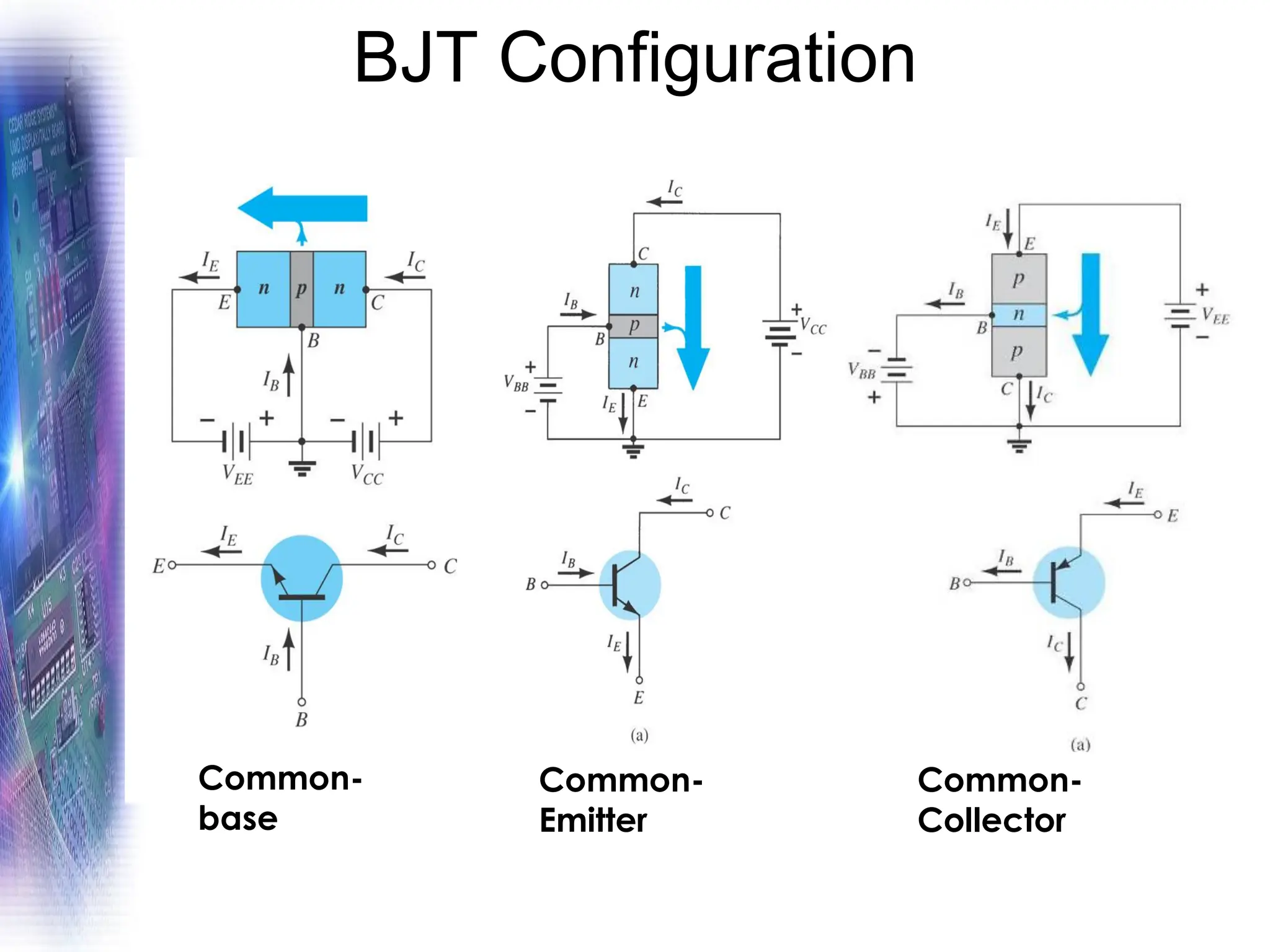
1. Dr. Awadh Al-Kubati
ELECTRONICS 1
University of Sana’a
Faculty of Engineering
Department of Biomedical Engineering
BIPOLAR JUNCTION TRANSISTOR
(BJT)
CHAPTER 3
2. BJT Structure
• BJT is constructed with 3 doped semiconductor regions
separated by 2 p-n junctions (Base-Collector & Base-
Emitter).
• 3 regions are called emitter, base and collector.
• Emitter (E) – most heavily doped region.
• Base (B) – thin and lightly doped region.
• Collector (C) – largest and moderately doped region.
3. BJT Structure
Biasing
Figure shows a bias arrangement for both NPN and PNP BJTs for
operation as an amplifier. Notice that in both cases the base-emitter
(BE) junction is forward-biased and the base-collector (BC) junction is
reverse-biased. This condition is called forward-reverse bias.
Forward-reverse bias of a BJT.
5. Operation
To understand how a transistor operates, let’s examine what happens inside the
NPN structure.
The heavily doped n-type emitter region has a very high density of
conduction-band (free) electrons, as indicated in (above figure) These free
electrons easily diffuse through the forward based BE junction into the
lightly doped and very thin p-type base region, as indicated by the wide arrow.
The base has a low density of holes, which are the majority carriers, as
represented by the white circles. A small percentage of the total number of free
electrons injected into the base region recombine with holes and move as
valence electrons through the base region and into the emitter region as hole
current, indicated by the red arrows.
When the electrons that have recombined with holes as valence electrons
leave the crystalline structure of the base, they become free electrons in the
metallic base lead and produce the external base current. Most of the free
electrons that have entered the base do not recombine with holes because the
base is very thin. As the free electrons move toward the reverse-biased BC
junction, they are swept across into the collector region by the attraction of
the positive collector supply voltage. The free electrons move through the
collector region, into the external circuit, and then return into the emitter
region along with the base current, as indicated. The emitter current is slightly
greater than the collector current because of the small base current that splits
off from the total current injected into the base region from the emitter.
7. BJT Operation
In normal operation, the base-emitter is forward-biased while
the base-collector is reverse-biased.
For NPN type, the collector is
more positive than the base,
which is more positive than
the emitter.
For PNP type, the voltages are
reversed to maintain the
forward-reverse bias.
8. Operation PNP transistor
Forward-biased junction Reverse-biased junction
IE = IC + IB
IC = IC majority + ICO (minority)
➢ ICO (minority) is called leakage
current
9. Operation NPN transistor
• heavily doped n-type emitter
region has a very high density of
free electrons.
• free electrons easily diffuse
through BE junction into lightly
doped and thin base region
• base has low density of
holes (majority carriers).
• electrons that have
recombined with holes
as valance electrons
leave the crystalline
structure of the base,
they become electrons
in the metallic base lead
and produce the
external base current.
• most free electrons don’t
recombine with holes as the base
is very thin→move toward BC
junction.
•Swept across into collector
region by attraction of +ve
supply.
• free electrons move through
collector region into external
circuit.
• then return into emitter region
along with the base current.
10. Transistor Currents
The directions of the currents in an NPN transistor and its schematic symbol
are as shown in Figure (a); those for a PNP transistor are shown in Figure (b).
Notice that the arrow on the emitter inside the transistor symbols points in the
direction of conventional current.
These diagrams show that the emitter current (IE) is the sum of the collector
current (IC) and the base current (IB), expressed as follows:
11. BJT Currents
IE = IC + IB
The emitter current is the sum of the collector current and the
small base current.
12. Basic Operation
• For both NPN and PNP transistors, VBB forward-biases the BE
junction and VCC reverse-biases the BC junction.
• Look at this one circuit as two separate circuits, the base-emitter
(left side) circuit and the collector-emitter (right side) circuit.
• Note that the emitter leg serves as a conductor for both circuits.
• The amount of current flow in the base-emitter circuit controls the
amount of current that flows in the collector circuit.
• Small changes in base-emitter current yields a large change in
collector-current.
• VBB – Base Supply Voltage
• VCC – Collector Supply Voltage
13. • The dc current gain of a transistor is the ratio of the dc collector
current (IC) to the dc base current (IB) and is designated dc beta
(DC ).
• Typical values of DC range from less than 20 to 200 or higher. DC is
usually designated as an equivalent hybrid (h) parameter, hFE, on
transistor datasheets. h-parameters are covered in Chapter 6. All you
need to know now is that
• The ratio of the dc collector current (IC) to the dc emitter current
(IE) is the dc alpha (DC ). The alpha is a less-used parameter than
beta in transistor circuits.
• Typically, values of DC range from 0.95 to 0.99 or greater, but DC is
always less than 1. The reason is that IC is always slightly less than
IE by the amount of IB. For example, if IE = 100 mA and IB = 1 mA, then
IC = 99 mA and DC = 0.99.
DC Beta (DC ) and DC Alpha (DC )
14.
15.
16. BJT Characteristics & Parameters
DC is usually equivalent hybrid (h) parameters hFE on transistor
datasheets.
hFE = DC
DC is ratio of collector current (IC) to the emitter current (IE). Less
used parameter than beta in transistor circuits.
DC = IC/IE
The collector characteristic
curves illustrate the relationship
of the 3 transistor currents. By
setting up other values of base
current, a family of collector
curves is develop. Beta() is the
ratio of collector current to
base current.
DC= IC/IB
17. Beta (β)
Relationship between amplification factors and
1
β
β
α
+
=
1
α
α
β
−
=
Relationship Between Currents
B
C βI
I = B
E 1)I
(β
I +
=
18. BJT Characteristics
• The beta for a transistor is not always constant.
• Temperature and collector current both affect beta, not to
mention the normal inconsistencies during the
manufacture of the transistor.
• There are also maximum power ratings to consider.
• The data sheet provides information on these
characteristics.
20. SOLUTION
1. Choose a base current near the center of the
range, in this case IB3.
2. Read the corresponding collector current.
3. Calculate the ratio.
167
30
5
=
=
=
A
mA
I
I
B
C
21. BJT Characteristics
• The collector characteristic curves show the relationship of the 3
transistor currents.
• Curve shown is for a fixed based current.
• Saturation region – collector current has reached a maximum and is
independent of the base current.
• Ideally, when VCE exceeds 0.7 V, the BC junction become reverse-biased
and transistor goes into active/linear region. IC increases very slightly as
VCE increases due to widening of BC depletion region.
• When VCE reaches a sufficiently high voltage, reverse-biased BC junction
goes into breakdown region; and IC increases rapidly as point C.
23. BJT Characteristics
• Cutoff – condition in which there is no base current,
IB=0 which results in only an extremely small leakage
current (ICEO) in the collector circuit. For practical
work, ICEO is assumed to be 0. So VCE = VCC.
In cutoff, neither the BE
junction nor the BC
junction are forward-
biased.
24. BJT Characteristics
• Saturation – condition in which there is maximum IC.
The saturation current is determined by the external
circuit (VCC and RC in this case) because the emitter-
collector voltage is minimum (≈0.2 V).
In saturation, an increase
of base current has no
effect on the collector
circuit and the relation
IC=βDCIB is no longer valid.
C
CE
CC
SAT
C
C
C
R
V
V
I
R
V
I
−
=
=
IC = βDC * IB
25. BJT Characteristics
• DC load line –
represent circuit that
is external to the
transistor. Drawn by
connecting saturation
and cutoff point.
26. EXAMPLE
1. What is the saturation current and the cutoff
voltage for the circuit?
2. Is the transistor saturated?
Assume VCE = 0.2 V in saturation.
28. BJT Configuration
There are three key dc voltages and three key dc currents to
be considered. Note that these measurements are important
for troubleshooting.
IB: DC base current
IE: DC emitter current
IC: DC collector current
VBE: DC voltage across
base-emitter junction
VCB: DC voltage across
collector-base junction
VCE: DC voltage from
collector to emitter
29. BJT Configuration
For proper operation the base-emitter junction is forward
biased by VBB and conducts just like a diode.
The collector-base junction is reverse biased by VCC and
blocks current flow through it’s junction just like a diode.
Remember current flow
through the base-emitter
junction will help establish
the path for current flow
from the collector to
emitter.
30. BJT Configuration
Analysis of this transistor circuit to predict the dc voltages and
currents requires use of Ohm’s law, Kirchhoff’s voltage law and
the beta for the transistor.
Analysis begins with the base circuit to determine the amount
of base current. Using Kirchhoff’s voltage law, subtract the
VBE = 0.7 and the remaining voltage is dropped across RB.
Determining the current for the base with this information is a
matter of applying of Ohm’s law.
The collector current is
determined by
multiplying the base
current by beta.
DC = IC/IB
IB = VRB/RB VRB = VBB - VBE
31. BJT Configuration
Base-Emitter (Forward Bias)
VBE = 0.7 will be used in most analysis examples.
B
BE
BB
B
BE
B
B
BB
R
V
V
I
V
R
I
V
−
=
=
−
− 0
BE
CE
CB
BE
B
B
BB
V
V
V
V
R
I
V
−
=
=
−
− 0
Collector - Emitter
B
DC
C
C
C
CC
CE
CE
C
C
CC
I
I
R
I
V
V
V
R
I
V
=
−
=
=
−
− 0
Collector – Base (Reverse Bias)
33. BJT Configuration
What we ultimately
determine by use of
Kirchhoff’s voltage law for
series circuits is that:
1. VBB is distributed across the
base-emitter junction and
RB in the base circuit.
2. VCC is distributed
proportionally across RC and
the transistor (VCE) in the
collector circuit.
35. BJT Amplifiers
• BJT amplifies AC signals by converting some of the DC
power from the power supplies to AC signal power.
• An AC signal at the input is superimposed in the dc bias
by the capacitive coupling.
• The output AC signal is inverted and rides on a DC level
of VCE.
36. BJT Switches
A transistor when used as a switch is simply being biased so
that it is in cutoff (switched off) or saturation (switched on).
Remember that the VCE in cutoff is VCC and 0V in saturation.
38. Troubleshooting
• Troubleshooting a live transistor circuit
requires us to be familiar with known good
voltages, but some general rules do apply.
• Certainly a solid fundamental understanding
of Ohm’s law and Kirchhoff’s voltage and
current laws is imperative (important).
• With live circuits it is most practical to
troubleshoot with voltage measurements.
39. Troubleshooting
Internal opens within the transistor
itself could also cause transistor
operation to cease.
Erroneous voltage measurements
that are typically low are a result of
point that is not “solidly
connected”. This called a floating
point. This is typically indicative of
an open.
Opens in the external resistors or connections of the base
or the collector circuit would cause current to cease (to
stop) in the collector and the voltage measurements
would indicate this.
40. Troubleshooting
Testing a transistor can be viewed more simply if you view it
as testing two diode junctions. Forward bias having low
resistance and reverse bias having infinite resistance.
41. Troubleshooting
The diode test function of a multimeter is more reliable than
using an ohmmeter. Make sure to note whether it is an NPN
or PNP and polarize the test leads accordingly.
42. Summary
➢ Bipolar Junction Transistor (BJT) is constructed of
three regions: base, collector, and emitter.
➢ BJT has two pn junctions, the base-emitter junction
and the base-collector junction.
➢ The two types of transistors are PNP and npn.
➢ For the BJT to operate as an amplifier, the base-
emitter junction is forward biased and the collector-
base junction is reverse biased.
➢ Of the three currents IB is very small in comparison to
IE and IC.
➢ Beta is the current gain of a transistor. This the ratio of
IC/IB.
43. Summary
➢ A transistor can be operated as an electronics
switch.
➢ When the transistor is off it is in cutoff condition (no
current).
➢ When the transistor is on, it is in saturation condition
(maximum current).
➢ Beta can vary with temperature and also varies
from transistor to transistor.