Download to read offline

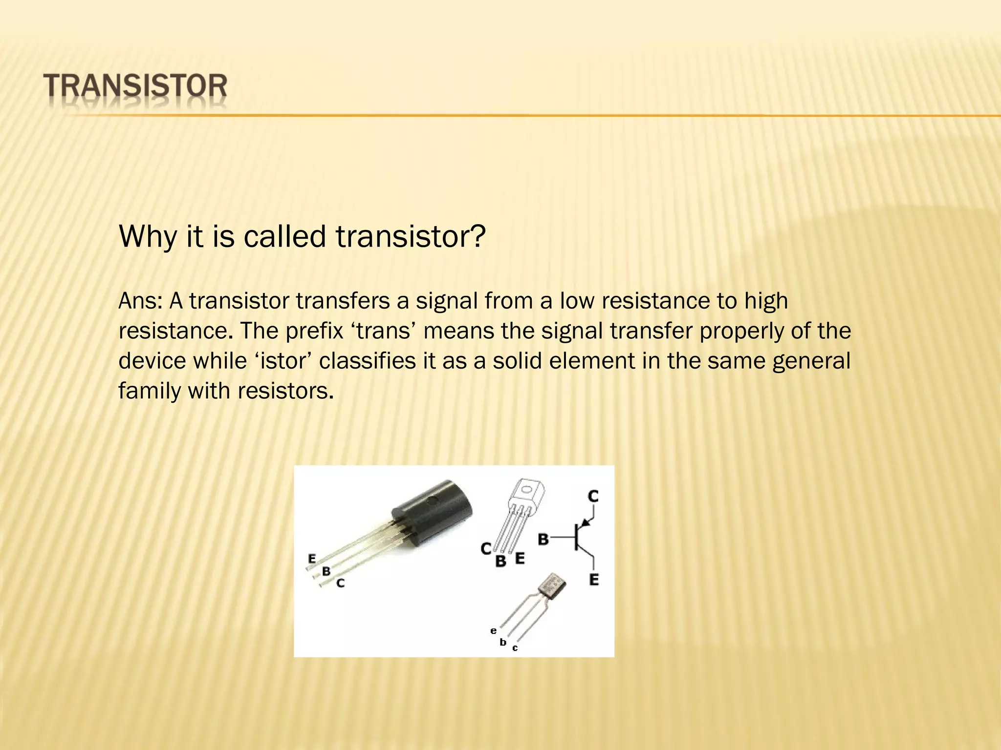


A transistor consists of a semiconductor with two pn junctions, forming either a PNP or NPN configuration. It transfers a signal from a low to high resistance, giving it the name "transistor". A transistor has three sections - the emitter supplies charge carriers, the collector collects the charges, and the base forms junctions between the emitter and collector. In an NPN transistor, a forward bias on the emitter-base junction causes electrons to flow from the emitter towards the base, with over 95% crossing into the collector to become the collector current.


![Transistor, fotodiode, dan diode pemencar [14]](https://cdn.slidesharecdn.com/ss_thumbnails/transistorfotodiodedandiodepemencar14-161106050358-thumbnail.jpg?width=640&height=640&fit=bounds)


