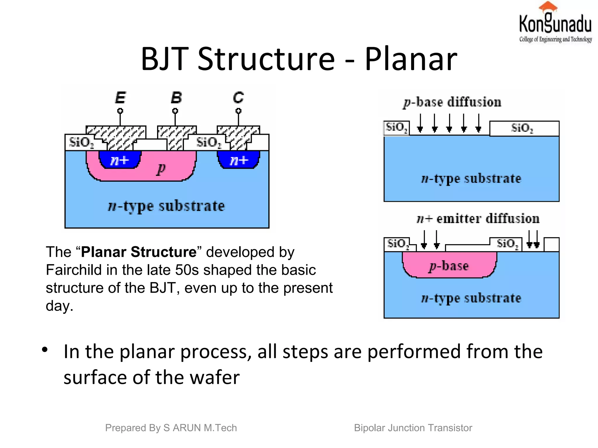
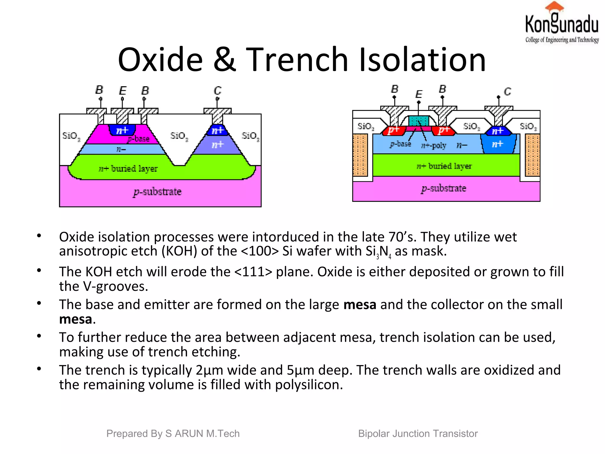
Bipolar Junction Transistors
(BJTBJT)
Contents
•Transistor
•The first transistor
•Symbol
•Fabrication
•Structure
•Oxide & Trench Isolation
•Double Poly Transistors
•Conclusion and Reference
1Prepared By S ARUN M.Tech Bipolar Junction Transistor
Transistors
• Two main categories of transistors:
–bipolar junction transistors (BJTs) and
–field effect transistors (FETs).
• Transistors have 3 terminals where the
application of current (BJT) or voltage (FET) to
the input terminal increases the amount of
charge in the active region.
• The physics of "transistor action" is quite
different for the BJT and FET.
Prepared By S ARUN M.Tech Bipolar Junction Transistor
The First Transistor: Point-contact transistor
A point-contact
transistor was the first
type of solid state
electronic transistor
ever constructed.
It was made by
researchers John
Bardeen & Walter
Houser Brattain at
Bell Laboratories in
December 1947.
Prepared By S ARUN M.Tech Bipolar Junction Transistor
Symbol
• A bipolar transistor
essentially consists of a pair of
PN Junction diodes that are
joined back-to-back.
• There are therefore two kinds
of BJT, the NPN and PNP
varieties.
• The three layers of the
sandwich are conventionally
called the Collector, Base, and
Emitter.
Prepared By S ARUN M.Tech Bipolar Junction Transistor
BJT Fabrication
• BJT can be made either as discrete
devices or in planar integrated form.
• In discrete, the substrate can be used for
one connection, typically the collector.
• In integrated version, all 3 contacts appear
on the top surface.
– The E-B diode is closer to the surface than
the B-C junction because it is easier make the
havier doping at the top.
Prepared By S ARUN M.Tech Bipolar Junction Transistor
BJT Structure - Discrete
• Early BJTs were fabricated using alloying - an complicated and
unreliable process.
• The structure contains two p-n diodes, one between the base
and the emitter, and one between the base and the collector.
Prepared By S ARUN M.Tech Bipolar Junction Transistor
BJT Structure - Planar
• In the planar process, all steps are performed from the
surface of the wafer
The “Planar Structure” developed by
Fairchild in the late 50s shaped the basic
structure of the BJT, even up to the present
day.
Prepared By S ARUN M.Tech Bipolar Junction Transistor
• BJTs are usually constructed vertically
– Controlling depth of the emitter’s n doping sets the base
width
Prepared By S ARUN M.Tech Bipolar Junction Transistor
Oxide & Trench Isolation
• Oxide isolation processes were intorduced in the late 70’s. They utilize wet
anisotropic etch (KOH) of the <100> Si wafer with Si3N4 as mask.
• The KOH etch will erode the <111> plane. Oxide is either deposited or grown to fill
the V-grooves.
• The base and emitter are formed on the large mesa and the collector on the small
mesa.
• To further reduce the area between adjacent mesa, trench isolation can be used,
making use of trench etching.
• The trench is typically 2µm wide and 5µm deep. The trench walls are oxidized and
the remaining volume is filled with polysilicon.
Prepared By S ARUN M.Tech Bipolar Junction Transistor
Double Poly Transistors
• A further extension of the self-aligned BJT structure is to use double
polysilicon (n+ for emitter, p+ for base) to reduce the area required
for contacts.
Prepared By S ARUN M.Tech Bipolar Junction Transistor
Conclusion
From this conclude that came to know about the
details structure of BJT
Reference
Balbir Kumar, Shail.B.Jain, “Electronic devices and
circuits” PHI learning private limited.
T.Joel, “Electronic Devices and Circuits”, Suchitra
publications.
Robert L.Boylestad, “Electronic devices and circuit
theory”
Prepared By S ARUN M.Tech Bipolar Junction Transistor

Bjt

  • 1.
    Bipolar Junction Transistors (BJTBJT) Contents •Transistor •Thefirst transistor •Symbol •Fabrication •Structure •Oxide & Trench Isolation •Double Poly Transistors •Conclusion and Reference 1Prepared By S ARUN M.Tech Bipolar Junction Transistor
  • 2.
    Transistors • Two maincategories of transistors: –bipolar junction transistors (BJTs) and –field effect transistors (FETs). • Transistors have 3 terminals where the application of current (BJT) or voltage (FET) to the input terminal increases the amount of charge in the active region. • The physics of "transistor action" is quite different for the BJT and FET. Prepared By S ARUN M.Tech Bipolar Junction Transistor
  • 3.
    The First Transistor:Point-contact transistor A point-contact transistor was the first type of solid state electronic transistor ever constructed. It was made by researchers John Bardeen & Walter Houser Brattain at Bell Laboratories in December 1947. Prepared By S ARUN M.Tech Bipolar Junction Transistor
  • 4.
    Symbol • A bipolartransistor essentially consists of a pair of PN Junction diodes that are joined back-to-back. • There are therefore two kinds of BJT, the NPN and PNP varieties. • The three layers of the sandwich are conventionally called the Collector, Base, and Emitter. Prepared By S ARUN M.Tech Bipolar Junction Transistor
  • 5.
    BJT Fabrication • BJTcan be made either as discrete devices or in planar integrated form. • In discrete, the substrate can be used for one connection, typically the collector. • In integrated version, all 3 contacts appear on the top surface. – The E-B diode is closer to the surface than the B-C junction because it is easier make the havier doping at the top. Prepared By S ARUN M.Tech Bipolar Junction Transistor
  • 6.
    BJT Structure -Discrete • Early BJTs were fabricated using alloying - an complicated and unreliable process. • The structure contains two p-n diodes, one between the base and the emitter, and one between the base and the collector. Prepared By S ARUN M.Tech Bipolar Junction Transistor
  • 7.
    BJT Structure -Planar • In the planar process, all steps are performed from the surface of the wafer The “Planar Structure” developed by Fairchild in the late 50s shaped the basic structure of the BJT, even up to the present day. Prepared By S ARUN M.Tech Bipolar Junction Transistor
  • 8.
    • BJTs areusually constructed vertically – Controlling depth of the emitter’s n doping sets the base width Prepared By S ARUN M.Tech Bipolar Junction Transistor
  • 9.
    Oxide & TrenchIsolation • Oxide isolation processes were intorduced in the late 70’s. They utilize wet anisotropic etch (KOH) of the <100> Si wafer with Si3N4 as mask. • The KOH etch will erode the <111> plane. Oxide is either deposited or grown to fill the V-grooves. • The base and emitter are formed on the large mesa and the collector on the small mesa. • To further reduce the area between adjacent mesa, trench isolation can be used, making use of trench etching. • The trench is typically 2µm wide and 5µm deep. The trench walls are oxidized and the remaining volume is filled with polysilicon. Prepared By S ARUN M.Tech Bipolar Junction Transistor
  • 10.
    Double Poly Transistors •A further extension of the self-aligned BJT structure is to use double polysilicon (n+ for emitter, p+ for base) to reduce the area required for contacts. Prepared By S ARUN M.Tech Bipolar Junction Transistor
  • 11.
    Conclusion From this concludethat came to know about the details structure of BJT Reference Balbir Kumar, Shail.B.Jain, “Electronic devices and circuits” PHI learning private limited. T.Joel, “Electronic Devices and Circuits”, Suchitra publications. Robert L.Boylestad, “Electronic devices and circuit theory” Prepared By S ARUN M.Tech Bipolar Junction Transistor