This document provides an overview of transistors, including:
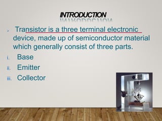
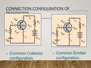
- Transistors have three parts - the base, emitter, and collector. The emitter supplies majority charge carriers, the collector collects them, and the base regulates carrier flow.
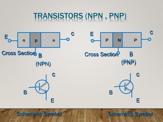
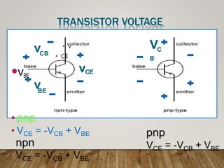
- There are two main types of transistors - NPN and PNP. They differ in whether holes or electrons are the majority carriers.
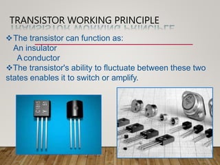
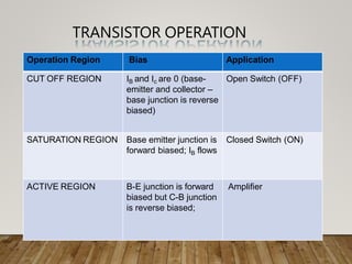
- Transistors can function as an insulator or conductor depending on biasing, enabling them to switch or amplify signals.
- Transistors have three operating regions - cut-off, saturation, and active - which determine how current and voltage are controlled at the junctions.