Download to read offline
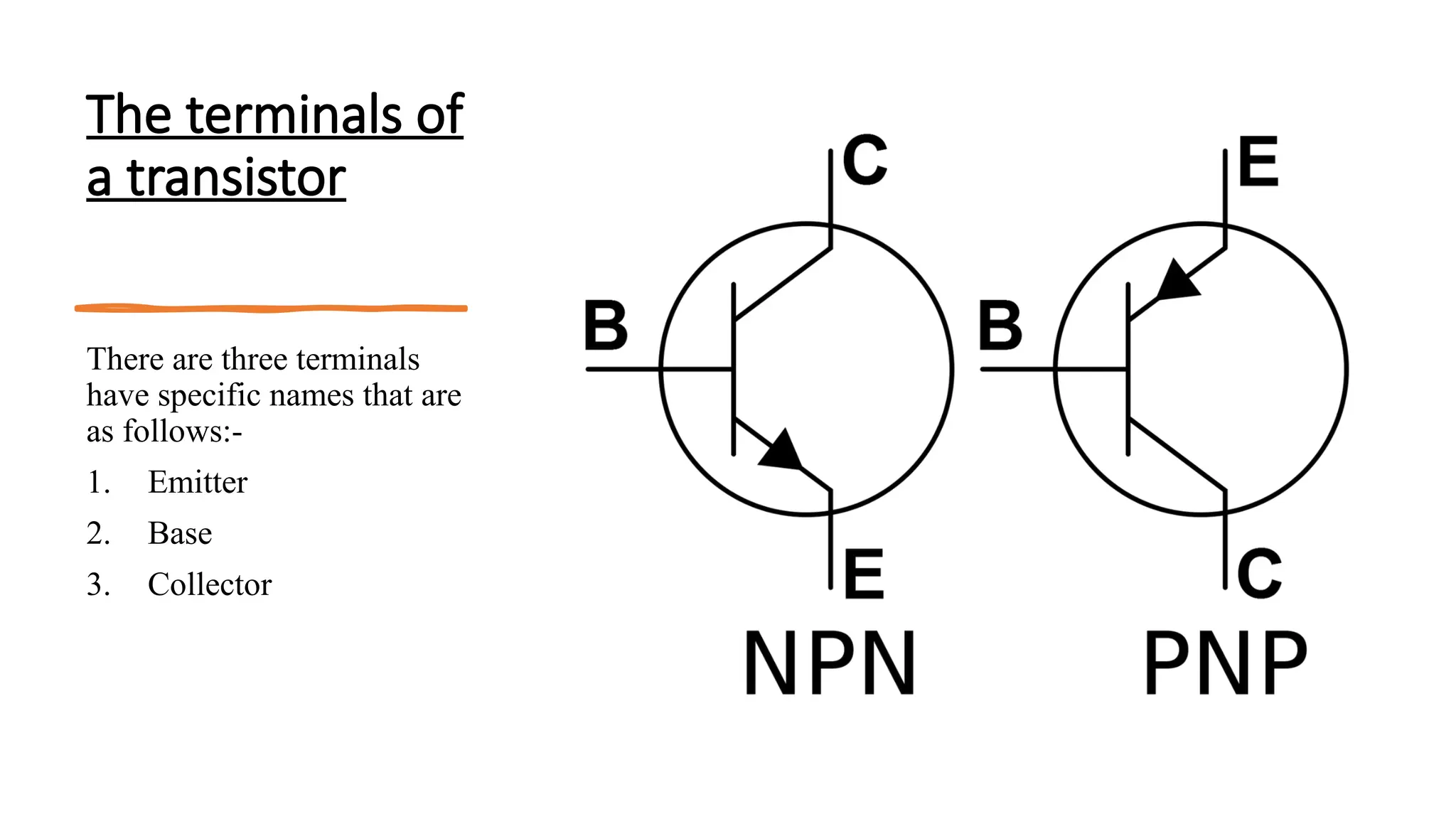
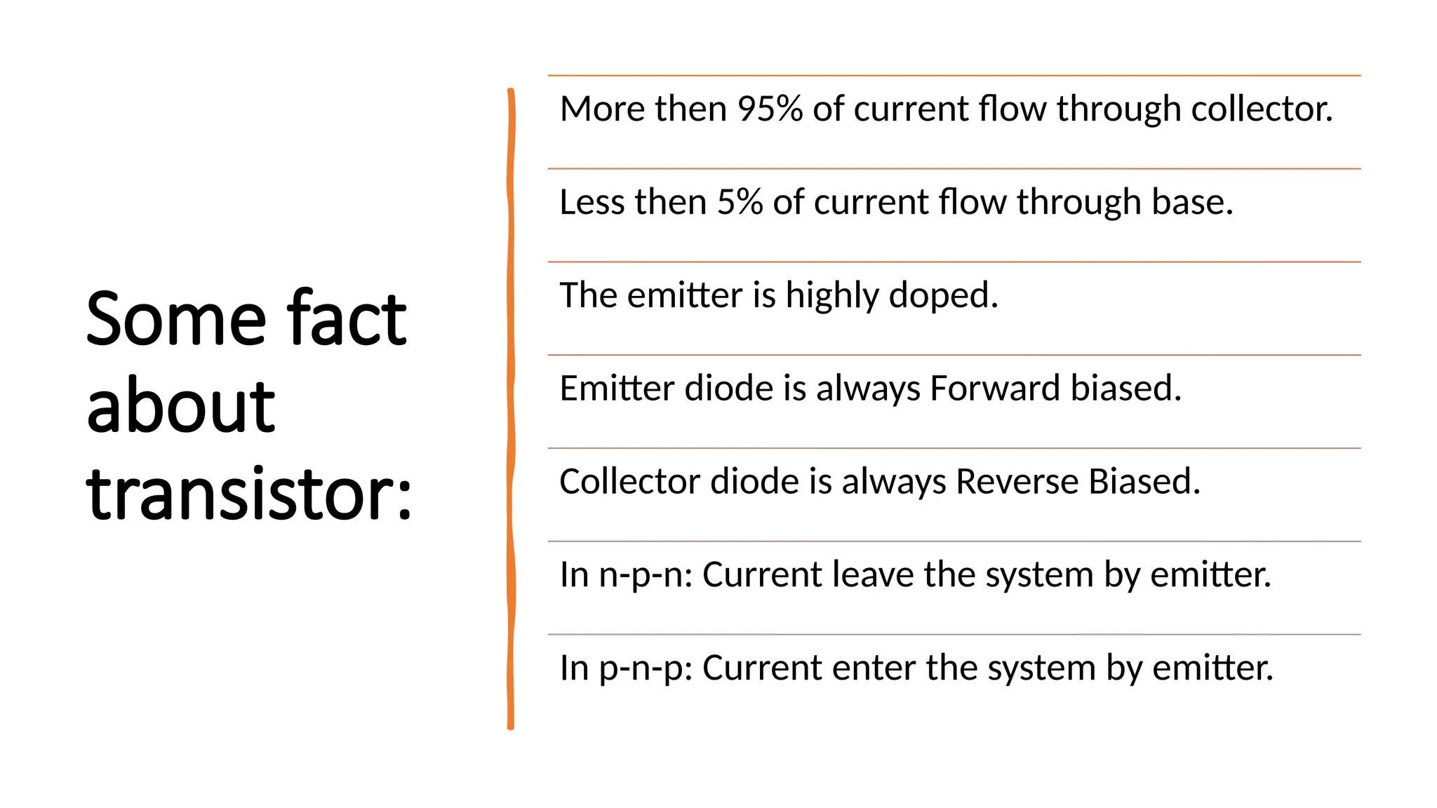


The document explains the structure and function of p-n-p and n-p-n transistors, highlighting the arrangement of semiconductor layers and their terminals: emitter, base, and collector. It describes the operation of each type of transistor, detailing how current flows through them with respect to their biasing conditions. Key points include the characteristics of the emitter, the role of the base current, and the behavior of the collector under reverse bias.