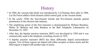
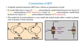
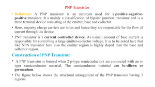
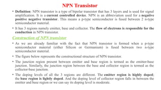
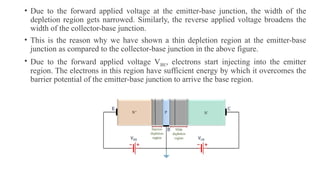
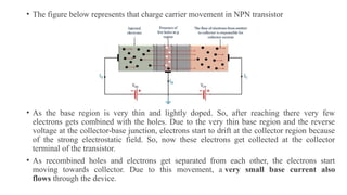
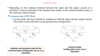
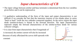
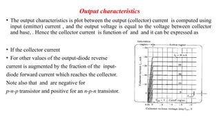
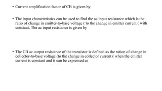
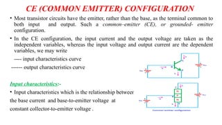
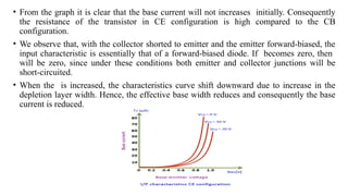
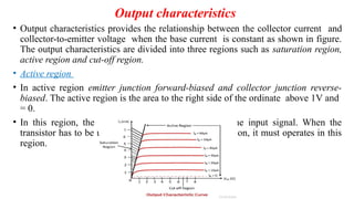
Bipolar Junction Transistor
(BJT)
Mr.KESANA GOPIKRISHNA
Assistant Professor
RGUKTN
Contents
• NPN and PNP junction transistor
• Characteristics of current flow across the base region
• Minority and Majority carrier profiles
• CB,CE and CC Configurations and their input and output characteristics.
• Comparison of CB,CE and CC characteristics.
• Junction biasing for saturation, cutoff and active region
• α and β parameters and the relation between them.
• Photo transistor
• Various biasing circuits
• Stabilizations
• Thermal runaway
• Thermal stability
• Transistor series and shunt voltage regulators.
History
• In 1904, the vacuum tube diode was introduced by J.A Fleming, there after in 1906,
Lee De Forest added a third element called control grid, to the vacuum diode.
• In the yearly 1930s the four-element tetrode and five-element pentode gained
prominence in the electron tube industry.
• The amplifying action of the first transistor is demonstrated by William Shockley,
Walter H. Brattain and John Bardeen at the Bell Telephone Laboratories on
December 23, 1947.
• After that, the bipolar junction transistor (BJT) was developed in 1950 and it was
commercially used in the telephone switching circuits in 1952.
• A bipolar junction transistor (BJT) has three differently doped semiconductor
regions. Two of these regions are doped with either acceptor or donor atoms and the
third region is doped with another type of atoms.
• Actually, a BJT consists of two PN-junctions which are placed back-
to-back.
• The word “bipolar” is used to state the role of both charge carriers
(electrons and holes).
• The term “transistor” is derived from the words ‘transfer’ and
‘resistor’ . These words describe the operation of a BJT which is the
transfer of an input signal from a low resistor circuit to a high
resistance circuit.
Construction of BJT
• A bipolar junction transistor (BJT) has a silicon or germanium crystal.
• It would either have a layer of N-type semiconductor sandwiched between two layers of
P-type semiconductor (PNP transistor), a layer of P-type semiconductor sandwiched
between two layers of N-type semiconductor material (NPN transistor).
• The sandwich of semiconductor is very small and sealed inside either a metal or plastic
case to protect it from moisture.
• Area:[C>E>B]
• The area of collector layer is largest. So it can dissipate heat quickly.
• Area of base layer is smallest and it is very thin layer.
• Area of emitter layer is medium.
• Doping level:[E>C>B]
• Collector layer is moderately doped. So it has medium number of charges.
• Base layer is lightly doped. So it has a very few number of charges.
• Emitter layer is heavily doped. So it has largest number of charges.
• Junctions:There are two junctions in this transistor
 Junction J-1: E-B Junction .
 Junction J-2: C-B Junction .
The two junctions have almost same potential barrier voltage of 0.6V to
0.7V, just like in a diode.
PNP Transistor
• Definition: A PNP transistor is an acronym used for a positive-negative-
positive transistor. It a mainly a classification of bipolar junction transistor and is a
three terminal device consisting of the emitter, base and collector.
• Here, majority charge carriers are holes and hence they are responsible for the flow of
current through the device.
• PNP transistor is a current controlled device. As a small amount of base current is
responsible for controlling a large emitter-collector voltage. It is to be noted here that
like NPN transistor here also the emitter region is highly doped than the base and
collector region.
Construction of PNP Transistor
• A PNP transistor is formed when 2 p-type semiconductors are connected with an n-
type semiconductor material. The semiconductor material can be silicon or
germanium.
• The figure below shows the structural arrangement of the PNP transistor having 3
regions:
• The three regions can be formed by either gaseous diffusion of p-type and n-type
impurities on a semiconductor wafer or by an epitaxial method, in which an intrinsic
region is grown on the heavily doped substrate of similar material.
• Here, the p region is heavily doped than the base and collector region. But the size
of the emitter region is greater than the base but comparatively smaller than the
collector.
• The base region is the thinnest among all and hence least doped. The collector
region has the largest area among all but is not doped as high as the emitter.
• a PNP transistor is also a back to back connection of
two diodes. The figure below shows the connection
of two diodes.
• But it is noteworthy here that, we cannot form a transistor by connecting two back to
back diodes. Now, the question appears why this is so?
• The answer to the above question is that we know that in order to ensure the proper
working of the transistor, the doping level of all the 3 regions must be sincerely taken into
consideration. But, by connecting two diodes only to have two pn junctions will not give
desired transistor operation.
• Also, a basic circuit arrangement of the transistor must have a configuration in such a
way that emitter-base junction must be forward biased and collector base junction to be
reverse biased in order to exhibit diffusion of carriers.
• Whereas, in the case of 2 back to back connected diodes, one junction will be forward
biased and other will be reverse biased. Hence, diffusion will not take place.
Working of PNP Transistor
• As we are already aware of the fact that a PNP transistor comprises 2 p regions and an n
region. Therefore, holes are the majority charge carriers and hence responsible for the
current conduction.
• Now, we will see how the flow of holes generates an electric current through the
transistor. The figure below shows the biasing arrangement of the PNP transistor
• Here, from the figure clearly indicates the emitter-base junction is provided with forward
voltage as p region is connected with positive and n region is connected with the negative
terminal of the battery.
• While the collector-base junction is biased
with reverse potential as the p region
showing collector is connected with the
negative terminal of the battery. This biasing
arrangement is necessary so as ensure the operation of the device in the active region.
• Let us now see how this biasing arrangement allows current conduction.
• As the emitter region is highly doped so the majority carriers of the p region i.e., holes
get repelled by the forward emitter-base voltage. This positive side of the battery applies
a repulsive force to the holes and they get sufficient energy and drift across the emitter-
base junction and reaches the base region.
• As the base region is not highly doped and consists of electrons as the region majority
carriers. Thus, only some of the holes reaching the base region combine with the
electrons of the base region. Rest, move towards the collector region.
• Also, there exists a depletion region due to the base-collector junction of the
transistor. The holes moving with high velocity due to the repulsive force of battery
VBE drift across the collector region.
• At the same time, the negative terminal of the battery VCB also attracts the positively
charged holes. The movement of holes in this way generates a large collector current
through the device.
• It is to be noted here that the emitter current IE is a combination of collector current,
IC and base current, IB. This is so because the combination of some of the holes with
the electrons of the base region also gives rise to small base current.
• Hence, the current equation is written as
NPN Transistor
• Definition: NPN transistor is a type of bipolar transistor that has 3 layers and is used for signal
amplification. It is a current controlled device. NPN is an abbreviation used for a negative
positive negative transistor. This means a p-type semiconductor is fused between 2 n-type
semiconductor material.
• It has 3 regions namely emitter, base and collector. The flow of electrons is responsible for the
conduction in NPN transistor.
Construction of NPN transistor
• As we are already familiar with the fact that NPN transistor is formed when a p-type
semiconductor material (either Silicon or Germanium) is fused between two n-type
semiconductor material.
• The figure below represents the constructional structure of NPN transistor.
• The junction region present between emitter and base region is termed as the emitter-base
junction. Similarly, the junction region between the base and collector region is termed as the
collector-base junction.
• The doping levels of all the 3 regions are different. The emitter region is highly doped;
the base region is lightly doped. And the doping level of collector region falls in between the
emitter and base region or we can say its doping level is moderate.
• It is noteworthy here that we cannot interchange the emitter and collector region. The
reason for this is that the thickness of the collector region is somewhat greater than the
emitter region. So, that it can dissipate more power.
Working of NPN transistor
• When the transistor is not provided with any applied bias or when no battery is
connected between its terminals. Then it is said to be the unbiased state of the transistor.
• We have already discussed how a PN junction diode operates under no biased condition.
And we already know that a transistor is formed by two PN junction.
• So, due to variation in temperature under no biased condition electrons in the emitter
region starts moving towards the base region. But, after a certain point of time a depletion
region is created at the emitter-base junction of the transistor.
• After reaching the base region only around 5% of electrons combine with the holes in this
region, rest drift across the collector region. Similarly, here also after some time a
depletion region is created at the base-collector junction of the transistor.
• It is to be noted here that the doping concentration of the material is responsible for the
thickness or thinness of the depletion region. More clearly, we can say that the width of
the depletion region will be more in case of a lightly doped region in comparison to the
highly doped region.
• This is the reason why we achieve broader depletion width at the collector-base
junction than the emitter-base junction.
• These two depletion regions act as the potential barrier for any further flow of majority
carriers.
• Moving further let us now understand the case when a voltage is applied to the terminals
of the transistor. Generally, the emitter-base junction is forward provided forward dc
voltage and the collector-base junction is supplied with a reverse dc voltage.
• Due to the forward applied voltage at the emitter-base junction, the width of the
depletion region gets narrowed. Similarly, the reverse applied voltage broadens the
width of the collector-base junction.
• This is the reason why we have shown a thin depletion region at the emitter-base
junction as compared to the collector-base junction in the above figure.
• Due to the forward applied voltage VBE, electrons start injecting into the emitter
region. The electrons in this region have sufficient energy by which it overcomes the
barrier potential of the emitter-base junction to arrive the base region.
• The figure below represents that charge carrier movement in NPN transistor
• As the base region is very thin and lightly doped. So, after reaching there very few
electrons gets combined with the holes. Due to the very thin base region and the reverse
voltage at the collector-base junction, electrons start to drift at the collector region because
of the strong electrostatic field. So, now these electrons get collected at the collector
terminal of the transistor.
• As recombined holes and electrons get separated from each other, the electrons start
moving towards collector. Due to this movement, a very small base current also
flows through the device.
• This is the reason why emitter current is the summation of base current and collector current.
• Applications of NPN transistor
1.As NPN transistors are used for signal amplification. Thus used in amplifying circuits.
2.It also finds its applications in logarithmic converters.
3.One of the major advantages of NPN transistor is its switching characteristic. Thus widely
used in switching applications.
4.These are also used in high-frequency applications.
Key Differences Between NPN and PNP Transistor
The factor that generates a key difference between NPN and PNP transistor is that in NPN
transistor due to sandwiching of p region between two n regions electrons are the majority
carriers. While in PNP transistor due to sandwiching of the n region between two p regions
holes acts as majority carriers.
In NPN transistors, the current flows from collector to emitter terminal i.e., opposite to the
direction of movement of electrons. As against, in PNP transistors, the current flows from
emitter to collector terminal.
In the symbolic representation of NPN transistor, an outward arrow from the
base towards emitter represents the direction of flow of current. However, the
symbolic representation of PNP transistor an inward arrow from emitter
towards base shows the direction of flow of current.
An NPN transistor exhibits faster frequency response as compared to a PNP
transistor.
In NPN transistor holes are the minority carriers while in PNP transistor
electrons are the minority carriers.
The conductivity level of NPN transistor is somewhat high as compared to
PNP transistor. This is so because electrons are more mobility than holes. So,
their movement in NPN transistor generates high conduction.
Also, the two types of BJT shows variation with respect to their biasing
arrangement. As the voltage provided to the emitter of NPN transistor is
negative and to that of PNP transistor is positive. Also, the voltage provided to
the collector of NPN transistor is positive and to that of PNP is negative.
Common-Base (CB) Configuration
• Depending on the common terminal between the input and the output circuits of a
transistor, it may be operated in the common-base mode, or the common-emitter mode, or
the common-collector mode.
Common-base (CB) Mode
 In this mode, the base terminal is common to both the input and the output circuits.
This mode is also referred to as the ground–base configuration.
Notation and symbols used for the
common-base configuration of a p–n–p
transistor
Common-base
configuration of an n–p–n
transistor
𝑉 𝐸𝐵 𝑉 𝐵𝐶 𝑉 𝐵𝐸 𝑉 𝐶𝐵
Input characteristics of CB
• The input voltage between emitter and base terminals is determined from the two variables
given below and it can be expressed as
• A qualitative understanding of the form of the input and output characteristics is not
difficult if we consider the fact that the transistor consists of two diodes place in series
“back to back” (with the two cathodes connected together). In the active region the input
diode (emitter-to-base) is biased in the forward direction. The input characteristics
represent simply the forward characteristics of the emitter-to-base diode for various
collector voltages.
• It is clear from input characteristics that if magnitude of
is increased, the emitter current will also be increased
(because of early effect)and the curves shift upwards with
constant.
Output characteristics
• The output characteristics is plot between the output (collector) current is computed using
input (emitter) current , and the output voltage is equal to the voltage between collector
and base, . Hence the collector current is function of and and it can be expressed as
• If the collector current
• For other values of the output-diode reverse
current is augmented by the fraction of the input-
diode forward current which reaches the collector.
Note also that and are negative for
p-n-p transistor and positive for an n-p-n transistor.
Active Region:
• In this region the collector junction is biased in reverse direction and emitter junction is
in forward direction.
• Consider first emitter current is zero, then the collector is small and is equal to the
reverse saturation current ( microampere for germanium and nano ampere for silicon) of
the collector junction considered as a diode.
• Suppose now that a forward emitter current is caused to flow in the emitter circuit. Then
a fraction -α of this current will reach to collector, and is given by
• In active region, collector current is essentially independent of collector voltage and
depends only upon the emitter current. However , because of early effect a small increase
in .
• Because is less than the unity, the magnitude of collector current is (slightly) less than
the emitter current.
Saturation Region :
• The region to left of the ordinate , and above the characteristics, in which both emitter
and collector junctions are forward –biased, is called the saturation region.
• We say that “bottoming” has taken place because the voltage has fallen near the bottom of the
characteristics where ≈0. actually, is slightly positive (for a p-n-p transistor) in this region ,
and this forward biasing of the collector accounts for the large change in collector current
with small change in collector voltage.
• For a forward bias, increases exponentially with voltage according to the diode relationship.
A forward bias means that the collector p material is made positive w.r.t the base n side , and
hence that hole current flows from the p side across the collector junction to the n material.
• This hole flow corresponds to a positive change in collector current. Hence the collector
current increases rapidly as indicated in Figure.
• may even becomes positive if the forward bias is sufficiently large.
Cutoff Region
• The characteristics for passes through the origin, but is otherwise similar to the other
characteristics. This characteristic is not coincident with the voltage axis, though the
separation is difficult to show because is only a few nanoamperes or microamperes.
• The region below the characteristic , for which the emitter and collector junctions are both
reverse-biased , is referred to as the cutoff region.
• Current amplification factor of CB is given by
• The input characteristics can be used to find the ac input resistance which is the
ratio of change in emitter-to-base voltage ( to the change in emitter current ( with
constant. The ac input resistance is given by
• The CB ac output resistance of the transistor is defined as the ration of change in
collector-to-base voltage (to the change in collector current ( when the emitter
current is constant and it can be expressed as
CE (COMMON EMITTER) CONFIGURATION
• Most transistor circuits have the emitter, rather than the base, as the terminal common to
both input and output. Such a common–emitter (CE), or grounded- emitter
configuration.
• In the CE configuration, the input current and the output voltage are taken as the
independent variables, whereas the input voltage and output current are the dependent
variables, we may write
---- input characteristics curve
------ output characteristics curve
Input characteristics:-
• Input characteristics which is the relationship between
the base current and base-to-emitter voltage at
constant collector-to-emitter voltage .
• From the graph it is clear that the base current will not increases initially. Consequently
the resistance of the transistor in CE configuration is high compared to the CB
configuration.
• We observe that, with the collector shorted to emitter and the emitter forward-biased, the
input characteristic is essentially that of a forward-biased diode. If becomes zero, then
will be zero, since under these conditions both emitter and collector junctions will be
short-circuited.
• When the is increased, the characteristics curve shift downward due to increase in the
depletion layer width. Hence, the effective base width reduces and consequently the base
current is reduced.
Output characteristics
• Output characteristics provides the relationship between the collector current and
collector-to-emitter voltage when the base current is constant as shown in figure.
The output characteristics are divided into three regions such as saturation region,
active region and cut-off region.
• Active region
• In active region emitter junction forward-biased and collector junction reverse-
biased. The active region is the area to the right side of the ordinate above 1V and
= 0.
• In this region, the transistor is very sensitive with the input signal. When the
transistor has to be used as an amplifier without distortion, it must operates in this
region.
• We now that
Combining above equation with then we get
If we define current amplification factor of CE is we can write the above equation as
Note that usually then in the active region.
• Cut-off Region:-
• In the cut-off region , the base current Then the emitter current is equal to collector
current . The collector current can be expressed as
• When the collector junction is reverse biased and base is open circuit, the collector current
is represented by .
• In the near cut-off region, the value of is about 0.9 for germanium transistor.
Consequently, the collector current is ten times the reverse saturation current (=10) at zero
base current.
• Therefore, the base current is not enough to operate transistor in the cut-off region. As
result, the emitter junction must be slightly reverse biased to operate the transistor in cut-
off region.
• At cut-off condition, the collector current must be equal to reverse saturation current and
the emitter current is equal to zero (
Saturation Region:-
• The transistor operates in the saturation region when the collector junction and the
emitter junction are forward biased by at least cut-in voltage.
• If is about a few tenths of a volt, is also a few tenths of a volt at saturation region.
• From the graph saturation region is very close to zero voltage axis, where all the curves
are merged and fall rapidly to origin. In the saturation region, the collector current is
independent of base current and it is equal to .
• The CE ac output resistance of the transistor is defined as the ration of change in
collector-to-emitter voltage (to the change in collector current ( when the base current is
constant and it can be expressed as
COMMON-COLLECTOR (CC) CONFIGURATION
• In the CC configuration, the input current and the output voltage are taken as the
independent variables, whereas the input voltage and output current are the dependent
variables, we may write
---- input characteristics curve
------ output characteristics curve
Input characteristics:-
• Input characteristics which is the relationship between
the base current and base-to-collector voltage at
constant emitter-to-collector voltage .
• The value of the output voltage VCE changes with respect to the input voltage VBC and
IB With the help of these values, input characteristic curve is drawn. The input
characteristic curve is shown below.
• To determine input characteristics, the emitter collector voltage is kept constant at
zero and base current is increased from zero by increasing .This is repeated for
higher fixed values of .A curve is drawn between base current and base emitter
voltage at constant collector base voltage is shown in figure
• Output characteristics
• It is defined as the characteristic curve drawn between output voltage to
output current whereas input current is constant.
• To determine output characteristics, the base current is kept constant at
zero and emitter current is increased from zero by increasing . This is
repeated for higher fixed values of
• The operation of all regions are same as
CE configuration.
Beee notes                   Best beee enotes

Beee notes Best beee enotes

  • 1.
    Bipolar Junction Transistor (BJT) Mr.KESANAGOPIKRISHNA Assistant Professor RGUKTN
  • 2.
    Contents • NPN andPNP junction transistor • Characteristics of current flow across the base region • Minority and Majority carrier profiles • CB,CE and CC Configurations and their input and output characteristics. • Comparison of CB,CE and CC characteristics. • Junction biasing for saturation, cutoff and active region • α and β parameters and the relation between them. • Photo transistor • Various biasing circuits • Stabilizations • Thermal runaway • Thermal stability • Transistor series and shunt voltage regulators.
  • 3.
    History • In 1904,the vacuum tube diode was introduced by J.A Fleming, there after in 1906, Lee De Forest added a third element called control grid, to the vacuum diode. • In the yearly 1930s the four-element tetrode and five-element pentode gained prominence in the electron tube industry. • The amplifying action of the first transistor is demonstrated by William Shockley, Walter H. Brattain and John Bardeen at the Bell Telephone Laboratories on December 23, 1947. • After that, the bipolar junction transistor (BJT) was developed in 1950 and it was commercially used in the telephone switching circuits in 1952. • A bipolar junction transistor (BJT) has three differently doped semiconductor regions. Two of these regions are doped with either acceptor or donor atoms and the third region is doped with another type of atoms.
  • 4.
    • Actually, aBJT consists of two PN-junctions which are placed back- to-back. • The word “bipolar” is used to state the role of both charge carriers (electrons and holes). • The term “transistor” is derived from the words ‘transfer’ and ‘resistor’ . These words describe the operation of a BJT which is the transfer of an input signal from a low resistor circuit to a high resistance circuit.
  • 5.
    Construction of BJT •A bipolar junction transistor (BJT) has a silicon or germanium crystal. • It would either have a layer of N-type semiconductor sandwiched between two layers of P-type semiconductor (PNP transistor), a layer of P-type semiconductor sandwiched between two layers of N-type semiconductor material (NPN transistor). • The sandwich of semiconductor is very small and sealed inside either a metal or plastic case to protect it from moisture.
  • 6.
    • Area:[C>E>B] • Thearea of collector layer is largest. So it can dissipate heat quickly. • Area of base layer is smallest and it is very thin layer. • Area of emitter layer is medium. • Doping level:[E>C>B] • Collector layer is moderately doped. So it has medium number of charges. • Base layer is lightly doped. So it has a very few number of charges. • Emitter layer is heavily doped. So it has largest number of charges. • Junctions:There are two junctions in this transistor  Junction J-1: E-B Junction .  Junction J-2: C-B Junction . The two junctions have almost same potential barrier voltage of 0.6V to 0.7V, just like in a diode.
  • 7.
    PNP Transistor • Definition:A PNP transistor is an acronym used for a positive-negative- positive transistor. It a mainly a classification of bipolar junction transistor and is a three terminal device consisting of the emitter, base and collector. • Here, majority charge carriers are holes and hence they are responsible for the flow of current through the device. • PNP transistor is a current controlled device. As a small amount of base current is responsible for controlling a large emitter-collector voltage. It is to be noted here that like NPN transistor here also the emitter region is highly doped than the base and collector region. Construction of PNP Transistor • A PNP transistor is formed when 2 p-type semiconductors are connected with an n- type semiconductor material. The semiconductor material can be silicon or germanium. • The figure below shows the structural arrangement of the PNP transistor having 3 regions:
  • 8.
    • The threeregions can be formed by either gaseous diffusion of p-type and n-type impurities on a semiconductor wafer or by an epitaxial method, in which an intrinsic region is grown on the heavily doped substrate of similar material. • Here, the p region is heavily doped than the base and collector region. But the size of the emitter region is greater than the base but comparatively smaller than the collector. • The base region is the thinnest among all and hence least doped. The collector region has the largest area among all but is not doped as high as the emitter. • a PNP transistor is also a back to back connection of two diodes. The figure below shows the connection of two diodes.
  • 9.
    • But itis noteworthy here that, we cannot form a transistor by connecting two back to back diodes. Now, the question appears why this is so? • The answer to the above question is that we know that in order to ensure the proper working of the transistor, the doping level of all the 3 regions must be sincerely taken into consideration. But, by connecting two diodes only to have two pn junctions will not give desired transistor operation. • Also, a basic circuit arrangement of the transistor must have a configuration in such a way that emitter-base junction must be forward biased and collector base junction to be reverse biased in order to exhibit diffusion of carriers. • Whereas, in the case of 2 back to back connected diodes, one junction will be forward biased and other will be reverse biased. Hence, diffusion will not take place. Working of PNP Transistor • As we are already aware of the fact that a PNP transistor comprises 2 p regions and an n region. Therefore, holes are the majority charge carriers and hence responsible for the current conduction. • Now, we will see how the flow of holes generates an electric current through the transistor. The figure below shows the biasing arrangement of the PNP transistor
  • 10.
    • Here, fromthe figure clearly indicates the emitter-base junction is provided with forward voltage as p region is connected with positive and n region is connected with the negative terminal of the battery. • While the collector-base junction is biased with reverse potential as the p region showing collector is connected with the negative terminal of the battery. This biasing arrangement is necessary so as ensure the operation of the device in the active region. • Let us now see how this biasing arrangement allows current conduction. • As the emitter region is highly doped so the majority carriers of the p region i.e., holes get repelled by the forward emitter-base voltage. This positive side of the battery applies a repulsive force to the holes and they get sufficient energy and drift across the emitter- base junction and reaches the base region. • As the base region is not highly doped and consists of electrons as the region majority carriers. Thus, only some of the holes reaching the base region combine with the electrons of the base region. Rest, move towards the collector region.
  • 11.
    • Also, thereexists a depletion region due to the base-collector junction of the transistor. The holes moving with high velocity due to the repulsive force of battery VBE drift across the collector region. • At the same time, the negative terminal of the battery VCB also attracts the positively charged holes. The movement of holes in this way generates a large collector current through the device. • It is to be noted here that the emitter current IE is a combination of collector current, IC and base current, IB. This is so because the combination of some of the holes with the electrons of the base region also gives rise to small base current. • Hence, the current equation is written as
  • 12.
    NPN Transistor • Definition:NPN transistor is a type of bipolar transistor that has 3 layers and is used for signal amplification. It is a current controlled device. NPN is an abbreviation used for a negative positive negative transistor. This means a p-type semiconductor is fused between 2 n-type semiconductor material. • It has 3 regions namely emitter, base and collector. The flow of electrons is responsible for the conduction in NPN transistor. Construction of NPN transistor • As we are already familiar with the fact that NPN transistor is formed when a p-type semiconductor material (either Silicon or Germanium) is fused between two n-type semiconductor material. • The figure below represents the constructional structure of NPN transistor. • The junction region present between emitter and base region is termed as the emitter-base junction. Similarly, the junction region between the base and collector region is termed as the collector-base junction. • The doping levels of all the 3 regions are different. The emitter region is highly doped; the base region is lightly doped. And the doping level of collector region falls in between the emitter and base region or we can say its doping level is moderate.
  • 13.
    • It isnoteworthy here that we cannot interchange the emitter and collector region. The reason for this is that the thickness of the collector region is somewhat greater than the emitter region. So, that it can dissipate more power. Working of NPN transistor • When the transistor is not provided with any applied bias or when no battery is connected between its terminals. Then it is said to be the unbiased state of the transistor. • We have already discussed how a PN junction diode operates under no biased condition. And we already know that a transistor is formed by two PN junction.
  • 14.
    • So, dueto variation in temperature under no biased condition electrons in the emitter region starts moving towards the base region. But, after a certain point of time a depletion region is created at the emitter-base junction of the transistor. • After reaching the base region only around 5% of electrons combine with the holes in this region, rest drift across the collector region. Similarly, here also after some time a depletion region is created at the base-collector junction of the transistor. • It is to be noted here that the doping concentration of the material is responsible for the thickness or thinness of the depletion region. More clearly, we can say that the width of the depletion region will be more in case of a lightly doped region in comparison to the highly doped region. • This is the reason why we achieve broader depletion width at the collector-base junction than the emitter-base junction. • These two depletion regions act as the potential barrier for any further flow of majority carriers. • Moving further let us now understand the case when a voltage is applied to the terminals of the transistor. Generally, the emitter-base junction is forward provided forward dc voltage and the collector-base junction is supplied with a reverse dc voltage.
  • 15.
    • Due tothe forward applied voltage at the emitter-base junction, the width of the depletion region gets narrowed. Similarly, the reverse applied voltage broadens the width of the collector-base junction. • This is the reason why we have shown a thin depletion region at the emitter-base junction as compared to the collector-base junction in the above figure. • Due to the forward applied voltage VBE, electrons start injecting into the emitter region. The electrons in this region have sufficient energy by which it overcomes the barrier potential of the emitter-base junction to arrive the base region.
  • 16.
    • The figurebelow represents that charge carrier movement in NPN transistor • As the base region is very thin and lightly doped. So, after reaching there very few electrons gets combined with the holes. Due to the very thin base region and the reverse voltage at the collector-base junction, electrons start to drift at the collector region because of the strong electrostatic field. So, now these electrons get collected at the collector terminal of the transistor. • As recombined holes and electrons get separated from each other, the electrons start moving towards collector. Due to this movement, a very small base current also flows through the device.
  • 17.
    • This isthe reason why emitter current is the summation of base current and collector current. • Applications of NPN transistor 1.As NPN transistors are used for signal amplification. Thus used in amplifying circuits. 2.It also finds its applications in logarithmic converters. 3.One of the major advantages of NPN transistor is its switching characteristic. Thus widely used in switching applications. 4.These are also used in high-frequency applications. Key Differences Between NPN and PNP Transistor The factor that generates a key difference between NPN and PNP transistor is that in NPN transistor due to sandwiching of p region between two n regions electrons are the majority carriers. While in PNP transistor due to sandwiching of the n region between two p regions holes acts as majority carriers. In NPN transistors, the current flows from collector to emitter terminal i.e., opposite to the direction of movement of electrons. As against, in PNP transistors, the current flows from emitter to collector terminal.
  • 18.
    In the symbolicrepresentation of NPN transistor, an outward arrow from the base towards emitter represents the direction of flow of current. However, the symbolic representation of PNP transistor an inward arrow from emitter towards base shows the direction of flow of current. An NPN transistor exhibits faster frequency response as compared to a PNP transistor. In NPN transistor holes are the minority carriers while in PNP transistor electrons are the minority carriers. The conductivity level of NPN transistor is somewhat high as compared to PNP transistor. This is so because electrons are more mobility than holes. So, their movement in NPN transistor generates high conduction. Also, the two types of BJT shows variation with respect to their biasing arrangement. As the voltage provided to the emitter of NPN transistor is negative and to that of PNP transistor is positive. Also, the voltage provided to the collector of NPN transistor is positive and to that of PNP is negative.
  • 19.
    Common-Base (CB) Configuration •Depending on the common terminal between the input and the output circuits of a transistor, it may be operated in the common-base mode, or the common-emitter mode, or the common-collector mode. Common-base (CB) Mode  In this mode, the base terminal is common to both the input and the output circuits. This mode is also referred to as the ground–base configuration. Notation and symbols used for the common-base configuration of a p–n–p transistor Common-base configuration of an n–p–n transistor 𝑉 𝐸𝐵 𝑉 𝐵𝐶 𝑉 𝐵𝐸 𝑉 𝐶𝐵
  • 20.
    Input characteristics ofCB • The input voltage between emitter and base terminals is determined from the two variables given below and it can be expressed as • A qualitative understanding of the form of the input and output characteristics is not difficult if we consider the fact that the transistor consists of two diodes place in series “back to back” (with the two cathodes connected together). In the active region the input diode (emitter-to-base) is biased in the forward direction. The input characteristics represent simply the forward characteristics of the emitter-to-base diode for various collector voltages. • It is clear from input characteristics that if magnitude of is increased, the emitter current will also be increased (because of early effect)and the curves shift upwards with constant.
  • 21.
    Output characteristics • Theoutput characteristics is plot between the output (collector) current is computed using input (emitter) current , and the output voltage is equal to the voltage between collector and base, . Hence the collector current is function of and and it can be expressed as • If the collector current • For other values of the output-diode reverse current is augmented by the fraction of the input- diode forward current which reaches the collector. Note also that and are negative for p-n-p transistor and positive for an n-p-n transistor.
  • 22.
    Active Region: • Inthis region the collector junction is biased in reverse direction and emitter junction is in forward direction. • Consider first emitter current is zero, then the collector is small and is equal to the reverse saturation current ( microampere for germanium and nano ampere for silicon) of the collector junction considered as a diode. • Suppose now that a forward emitter current is caused to flow in the emitter circuit. Then a fraction -α of this current will reach to collector, and is given by • In active region, collector current is essentially independent of collector voltage and depends only upon the emitter current. However , because of early effect a small increase in . • Because is less than the unity, the magnitude of collector current is (slightly) less than the emitter current. Saturation Region : • The region to left of the ordinate , and above the characteristics, in which both emitter and collector junctions are forward –biased, is called the saturation region.
  • 23.
    • We saythat “bottoming” has taken place because the voltage has fallen near the bottom of the characteristics where ≈0. actually, is slightly positive (for a p-n-p transistor) in this region , and this forward biasing of the collector accounts for the large change in collector current with small change in collector voltage. • For a forward bias, increases exponentially with voltage according to the diode relationship. A forward bias means that the collector p material is made positive w.r.t the base n side , and hence that hole current flows from the p side across the collector junction to the n material. • This hole flow corresponds to a positive change in collector current. Hence the collector current increases rapidly as indicated in Figure. • may even becomes positive if the forward bias is sufficiently large. Cutoff Region • The characteristics for passes through the origin, but is otherwise similar to the other characteristics. This characteristic is not coincident with the voltage axis, though the separation is difficult to show because is only a few nanoamperes or microamperes. • The region below the characteristic , for which the emitter and collector junctions are both reverse-biased , is referred to as the cutoff region.
  • 24.
    • Current amplificationfactor of CB is given by • The input characteristics can be used to find the ac input resistance which is the ratio of change in emitter-to-base voltage ( to the change in emitter current ( with constant. The ac input resistance is given by • The CB ac output resistance of the transistor is defined as the ration of change in collector-to-base voltage (to the change in collector current ( when the emitter current is constant and it can be expressed as
  • 25.
    CE (COMMON EMITTER)CONFIGURATION • Most transistor circuits have the emitter, rather than the base, as the terminal common to both input and output. Such a common–emitter (CE), or grounded- emitter configuration. • In the CE configuration, the input current and the output voltage are taken as the independent variables, whereas the input voltage and output current are the dependent variables, we may write ---- input characteristics curve ------ output characteristics curve Input characteristics:- • Input characteristics which is the relationship between the base current and base-to-emitter voltage at constant collector-to-emitter voltage .
  • 26.
    • From thegraph it is clear that the base current will not increases initially. Consequently the resistance of the transistor in CE configuration is high compared to the CB configuration. • We observe that, with the collector shorted to emitter and the emitter forward-biased, the input characteristic is essentially that of a forward-biased diode. If becomes zero, then will be zero, since under these conditions both emitter and collector junctions will be short-circuited. • When the is increased, the characteristics curve shift downward due to increase in the depletion layer width. Hence, the effective base width reduces and consequently the base current is reduced.
  • 27.
    Output characteristics • Outputcharacteristics provides the relationship between the collector current and collector-to-emitter voltage when the base current is constant as shown in figure. The output characteristics are divided into three regions such as saturation region, active region and cut-off region. • Active region • In active region emitter junction forward-biased and collector junction reverse- biased. The active region is the area to the right side of the ordinate above 1V and = 0. • In this region, the transistor is very sensitive with the input signal. When the transistor has to be used as an amplifier without distortion, it must operates in this region.
  • 28.
    • We nowthat Combining above equation with then we get If we define current amplification factor of CE is we can write the above equation as Note that usually then in the active region.
  • 29.
    • Cut-off Region:- •In the cut-off region , the base current Then the emitter current is equal to collector current . The collector current can be expressed as • When the collector junction is reverse biased and base is open circuit, the collector current is represented by . • In the near cut-off region, the value of is about 0.9 for germanium transistor. Consequently, the collector current is ten times the reverse saturation current (=10) at zero base current. • Therefore, the base current is not enough to operate transistor in the cut-off region. As result, the emitter junction must be slightly reverse biased to operate the transistor in cut- off region. • At cut-off condition, the collector current must be equal to reverse saturation current and the emitter current is equal to zero (
  • 30.
    Saturation Region:- • Thetransistor operates in the saturation region when the collector junction and the emitter junction are forward biased by at least cut-in voltage. • If is about a few tenths of a volt, is also a few tenths of a volt at saturation region. • From the graph saturation region is very close to zero voltage axis, where all the curves are merged and fall rapidly to origin. In the saturation region, the collector current is independent of base current and it is equal to . • The CE ac output resistance of the transistor is defined as the ration of change in collector-to-emitter voltage (to the change in collector current ( when the base current is constant and it can be expressed as
  • 31.
    COMMON-COLLECTOR (CC) CONFIGURATION •In the CC configuration, the input current and the output voltage are taken as the independent variables, whereas the input voltage and output current are the dependent variables, we may write ---- input characteristics curve ------ output characteristics curve Input characteristics:- • Input characteristics which is the relationship between the base current and base-to-collector voltage at constant emitter-to-collector voltage . • The value of the output voltage VCE changes with respect to the input voltage VBC and IB With the help of these values, input characteristic curve is drawn. The input characteristic curve is shown below.
  • 32.
    • To determineinput characteristics, the emitter collector voltage is kept constant at zero and base current is increased from zero by increasing .This is repeated for higher fixed values of .A curve is drawn between base current and base emitter voltage at constant collector base voltage is shown in figure
  • 33.
    • Output characteristics •It is defined as the characteristic curve drawn between output voltage to output current whereas input current is constant. • To determine output characteristics, the base current is kept constant at zero and emitter current is increased from zero by increasing . This is repeated for higher fixed values of • The operation of all regions are same as CE configuration.